Sign In
Upload
Manuals
Brands
Dialog Semiconductor Manuals
Microcontrollers
DA14580
Dialog Semiconductor DA14580 Bluetooth Manuals
Manuals and User Guides for Dialog Semiconductor DA14580 Bluetooth. We have
4
Dialog Semiconductor DA14580 Bluetooth manuals available for free PDF download: User Manual
Dialog Semiconductor DA14580 User Manual (57 pages)
Getting started with Development Kit - Basic
Brand:
Dialog Semiconductor
| Category:
Microcontrollers
| Size: 4 MB
Table of Contents
Abstract
1
Contents
2
Table of Contents
2
Figures
3
Tables
4
1 Terms and Definitions
4
2 References
5
3 Introduction
6
Hardware Content
6
Figure 1: DEVKT - Basic Kit
6
Table 1: Content of the DEVKT - Basic Kit
6
Basic Development Kit for Da1458X Family
7
Differences between DA14580, DA14581, DA14583, DA14585 and DA14586
7
Table 2: DA14580
7
Table 3: DA14581
7
Table 4: DA14583
8
Table 5: DA14585
8
Table 6: DA14586
9
Software Development Tools
10
Smartsnippets Studio Introduction
10
Installation
10
Figure 2: Smartsnippets Studio Platform
10
Starting Smartsnippets Studio
11
Figure 3: Dialog for Selecting Workspace
11
Figure 4: SDK Tools Installer
11
Setting up Your PC
12
Smartsnippets Studio
12
Table 7: Installation Tools and Drivers
12
Tera Term
13
Software Development Kit Content
14
Tools
14
SDK Documents
14
SDK Source Code Examples (Created with Keil IDE)
14
Figure 5: DA14580 Target Selection
15
Figure 6: Da14585 Target Selection
15
Table 8: SDK Examples
15
Figure 7: DA14580 USB Selection
16
Figure 8: DA14585 USB Selection
16
Pinning
18
DA14580 Pin Assignment
18
DA14581 Pin Assignment
18
Figure 9: DA14580 - QFN48 (Left) and QFN40 (Right) Pin Assignment
18
Figure 10: DA14581- QFN40 Pin Assignment
18
DA14583 Pin Assignment
19
Figure 11: QFN40 Pin Assignment from Datasheet
19
Table 9: SPI Connections
19
DA14585 Pin Assignment
20
Figure 12: DA14585 - QFN40 Pin Assignment
20
DA14586 Pin Assignment
21
Figure 13: DA14586 - QFN40 Pin Assignment
21
Table 10: SPI Connections
21
PCB Design and Functionalities
22
Da14581Devkt-B (228-01-A)
22
Figure 14: Components on PCB Top Layer of the Da14580/581Basic Kit
22
Figure 15: Topview of PCB DA14580/581 with Components and Functionalities
22
Da14583Devkt-B (285-02-A)
23
Figure 16: Components on PCB Top Layer of the DA14583 Basic Kit
23
Figure 17: Topview of PCB DA14583 with Components and Functionalities
23
Da1458Xdevkt-B (321-04-A)
24
Figure 18: Da1458X DEKT-B Block Diagram
24
Figure 19: Components on PCB Top Layer of the DA14585/6 Basic Kit (321-04-A)
24
Schematics and Layouts
25
DA14580DEVKT-B Schematic
25
Figure 20: Topview of PCB Da1458X with Components and Functionalities
25
Figure 21: DA14580DEVKT-B_Vb Part 1
26
Figure 22: DA14580DEVKT-B_Vb Part 2
27
DA14581DEVKT-B_Va Schematic
28
Figure 23: DA1581DEVKT-B_Va Part 1
28
Figure 24: DA1581DEVKT-B_Va Part 2
29
DA14583DEVKT-B_Va Schematic
30
Figure 25: DA1583DEVKT-B_Va Part 1
30
Figure 26: DA1583DEVKT-B_Va Part 2
31
Da1458Xdevkt-B (321-04-A) Schematic
32
Figure 27: Da158Xdevkt-B_Va Part 1
32
Figure 28: Da158Xdevkt-B_Va Part 2
33
Configuring Basic Development Kit-Board by Jumper Settings
34
3.9.1 Configuring the DA14580/581 Basic Kit-Board by Jumper Settings
34
Figure 29: DA14580/581 (Fabrication Default) UART Boot Settings (Tx P0_4 and Rx P0_5)
34
Figure 30: Da14580/581Boot from External SPI Memory
34
Figure 31: Data Direction of UART Within J4
34
3.9.2 Configuring the DA14583 Basic Kit-Board by Jumper Settings
35
Figure 32: DA14580/581 Layout of Headers J4 and J6
35
Figure 33: (Fabrication Default) DA14583 UART Boot Settings (Tx P0_4 and Rx P0_5)
35
Figure 34: Data Direction of UART Within J4
35
Figure 35: DA14583 Layout of Headers J4 and J6
36
3.9.3 Configuring the Da1458X Basic Kit-Board by Jumper Settings
37
Figure 36: Da1458X Layout of Headers J4 and J6
37
Figure 37: Da1458X (Fabrication Default) UART Boot Settings (Tx P0_4 and Rx P0_5)
37
Figure 38: Data Direction of UART Within J4
38
Figure 39: Da1458X Boot from External SPI Memory. It Is Valid for DA14580/1/5 (Add Photo)
38
3.10 Block Diagram & Downloading Software
39
Figure 40: Block Diagram with Different Memory Locations
39
Figure 41: DA14585/586 Block Diagram
40
4 Using the Demo Kit
41
Run an Example on the DA14580/581/583/585/586
41
Table 11: Run an Example on DA14580/581/583/585/586
41
Figure 42: Setup of DA14580/581/585 DEVKT - BASIC During Power Measurement
45
Figure 43: Setup of DA14583/586 DEVKT - BASIC During Power Measurement
45
5 Power Management: Measuring Current
45
Layout DA14580/581
47
Connections of J10 and J11
47
Figure 44: a General Overview of the DA14581 Development Board
47
Figure 45: DA14580/581 Connection Diagram of J10 and J11
47
Layout DA14583
48
Connections of J10
48
Figure 46: a General Overview of the DA14583 Development Board
48
Figure 47: DA14583 Connection Diagram of J10
48
Um-B
48
Using the Smart Snippets CLI
49
Figure 48: Open the CLI of Smartsnippets
49
Figure 49: Smartsnippets Output
49
Blinky' Test Software
50
Latency Timer of FTDI Cable
52
Figure 50: FTDI Latency Timer
52
Da1458Xdevkt-B Hardware Differences to DA14580, DA14581 and DA14583 Hardware Versions
53
Table 12: Da1458Xdevkt-B Differences to Previous Hardware Versions
53
Da1458Xdevkt-B BOM Modifications for Supporting Da1458X Soc Family
54
Table 13: Da1458X BOM Modifications for Enabling Da1458X Family Chips
54
Figure 51: Location of the Components that Enables Various Versions of Da1458X Family
55
Figure 52: Configuration Components for Enabling the Various Versions of Da1458X Family
55
6 Web-Links
56
Revision History
56
Advertisement
Dialog Semiconductor DA14580 User Manual (63 pages)
Brand:
Dialog Semiconductor
| Category:
Microcontrollers
| Size: 4 MB
Table of Contents
Abstract
1
Table of Contents
2
Contents
2
Tables
3
Figures
3
Terms and Definitions
5
References
5
Introduction
6
Order Content
7
Figure 1: Overview of All DEVKT -Pro Parts
7
Table 1: Content of the DA14580/581/583 Pro Kit. Ordernumbers Are Made Bold
8
3.2 Pro Kit for Da1458X Family
9
3.2.1 Differences between DA14580, DA14581, DA14583, DA14585 and DA14586
9
Table 2: DA14580
9
Table 3: DA14581
9
Table 4: DA14583
10
Table 5: DA14585
10
Table 6: DA14586
11
Software Development Tools
12
Smartsnippets Introduction
12
Installation
12
Figure 2: Smartsnippets Studio Platform
12
Starting Smartsnippets Studio
13
Figure 3: Dialog for Selecting Workspace
13
Figure 4: SDK Tools Installer
13
Setting up Your PC
14
Smartsnippets Studio
14
Table 7: Installation Tools and Drivers
14
Tera Term
15
3.4.3 Software Development Kit Content
16
Table 8: SDK Examples
17
Figure 5: DA14580 Target Selection
17
Figure 6: Da14585 Target Selection
18
Figure 7: DA14580 USB Selection
18
Figure 8: DA14585 USB Selection
18
Pinning
20
Table 9: SPI Connections
20
Figure 9: QFN40 Pin Assignment from Datasheet
20
DA14585 Pining
21
Figure 10: DA14585 - QFN40 Pin Assignment
21
DA14586 Pining
22
Table 10: SPI Connections
22
Figure 11: DA14586 - QFN40 Pin Assignment
22
3.7.1 PCB Design and Functionalities
23
Figure 12: Motherboard of Development Kit - Pro (PCB Topview)
23
3.7.2 Configuring the Pro Kit-Board by Jumper Settings
24
Figure 13: DA14580/581/583 (Fabrication Default) UART Boot Settings (T_Txd : (P0_5) and T_Rxd : (P0_4))
24
Figure 14: DA14580/581 Boot from External SPI Memory
24
Figure 15: DA14583 Boot from Internal SPI Memory
25
Figure 16: Layout of Headers J5 and J6
25
Figure 17: UART Data Direction of Uart Within J5
25
3.7.3 Block Diagram
26
Figure 18: Block Diagram of Total Systemmemory and Tools
27
Figure 19: DA14580/581/583 Block Diagram
28
Figure 20: DA14585/586 Block Diagram
29
Using the Demo Kit
30
Run an Example on the DA14580/581/583
30
Table 11: Run an Example on DA14580/581/583
30
Layout
35
Connections of J7 and J8
35
Figure 21: Board Layout
35
Figure 22: IO Breakout Available on QFN40 and QFN48
35
Figure 23: IO Breakout Available on QFN48
35
Schematics Motherboard and Daughterboards
36
Peripherals
36
Figure 24: Peripherals Schematic of Motherboard
36
SPI and Serial
37
Figure 25: SPI and Serial Schematic of Motherboard
37
Current Measurement
38
Figure 26: Current Measurement Schematic of Motherboard
38
JTAG Interface
39
Figure 27: JTAG Interface Schematic of Motherboard
39
PCI-E
40
Figure 28: PCI-E Schematic of Motherboard
40
Power Supplies
41
Figure 29: Power Supplies Schematics of Motherboard
41
USB HUB Controller
42
Figure 30: USB HUB Controller Schematic of Motherboard
42
DA14580 WLCSP Daughter Board
43
Figure 31: DA14580 WLCSP Daughter Board
43
DA14580 QFN40 Daughterboard
44
Figure 32: DA14580 QFN40 Daughterboard
44
C.10 DA14580 QFN48 Daughterboard
45
Figure 33: DA14580 QFN48 Daughterboard
45
C.11 DA14581 WLCSP Daughterboard
46
Figure 34: DA14581 WLCSP Daughterboard
46
C.12 DA14581 QFN40 Daughterboard
47
Figure 35: DA14581 QFN40 Daughterboard
47
C.13 DA14583 QFN40 Daughterboard
48
Figure 36: DA14583 QFN40 Daughterboard
48
DA14585 WLCSP34 Daughterboard (321-3-X)
49
Figure 37: DA14585 WLCSP34 Daughterboard
49
DA14585 QFN40 Daughterboard (321-2-X)
50
Figure 38: DA14585 QFN40 Daughterboard
50
DA14586 QFN40 Daughterboard (321-2-X)
51
Table 12: BOM Diifferences between DA14585 and DA14586 Designs
51
Figure 39: DA14586 QFN40 Daughterboard
51
Using the Smartsnippets CLI
52
Figure 40: Smartsnippets HELP
52
Figure 41: Open the CLI of Smartsnippets
52
Figure 42: Smart Snippet CMD Window
53
Latency Timer of FTDI Cable
54
Figure 43: FTDI Latency Timer
54
RF-Testing DEVKT - Pro
55
Battery Connection 'Workaround
57
Figure 44: Reset Circuitry. R84 to be Dismounted
57
Figure 45: Location of R84
57
Power Bouncing Workaround
58
Figure 46: PRO-Motherboard Power Jumper
58
Web-Link
59
Figure 47: DA14585/6 QFN40 Daughterboard (321-10-X)
59
Revision History
60
Dialog Semiconductor DA14580 User Manual (49 pages)
Smart development Kit – Pro
Brand:
Dialog Semiconductor
| Category:
Accessories
| Size: 3 MB
Table of Contents
Abstract
1
Contents
2
Table of Contents
2
Figures
3
Tables
3
1 Terms and Definitions
4
2 References
4
3 Introduction
5
Hardware Content
6
Figure 1: DA14580/581 - Pro Kit
6
Figure 2: DA14583 - Pro Kit
6
Table 1: Content of the DA14580/581/583 Pro Kit
7
Web Content
8
Software Development Kit Content
8
Tools
8
SDK Documents
8
SDK Source Code Examples (Created in Keil)
9
DA14580 - DA14581 Pro Kit
11
Differences between the DA14580, DA14581 and DA14583
11
Table 2: DA14580
11
Table 3: DA14581
11
Table 4: DA14583
12
Pinning
13
Figure 3: QFN40 Pin Assignment from Datasheet
13
Table 5: SPI Connections
13
Figure 4: DA14580 Development Kit - Pro (PCB Topview)
14
PCB Design and Functionalities
14
Configuring the Pro Kit-Board by Jumper Settings
15
Figure 6: DA14580/581 Boot from External SPI Memory
15
P0_4
16
Figure 7: DA14583 Boot from Internal SPI Memory
16
Figure 8: Layout of Headers J5 and J6
16
Figure 9: UART Data Direction of Uart Within J5
16
Block Diagram
17
Figure 10: Block Diagram of Total System
17
4 Installation of Tools and Drivers
18
Keil
18
Table 6: Installation Tools and Drivers
18
SEGGER Jlink Driver
19
FTDI Driver
20
Tera Term
20
5 Memory and Tools
21
Figure 11: DA14580/581/583 Block Diagram
21
6 Using the Demo Kit
22
Run an Example on DA14580/581/583
22
Table 7: Run an Example on DA14580/581/583
22
Connections of J7 and J8
27
Figure 12: Board Layout
27
Figure 13: IO Breakout Available on QFN40 and QFN48
27
Figure 14: IO Breakout Available on QFN48
27
Layout
27
Schematics Motherboard and Daughterboards
28
Peripherals
28
Figure 15: Peripherals Schematic of Motherboard
28
SPI and Serial
29
Figure 16: SPI and Serial Schematic of Motherboard
29
Current Measurement
30
Figure 17: Current Measurement Schematic of Motherboard
30
C.3 Current Measurement
30
JTAG Interface
31
Figure 18: JTAG Interface Schematic of Motherboard
31
C.4 JTAG Interface
31
PCI-E
32
Figure 19: PCI-E Schematic of Motherboard
32
C.5 PCI-E
32
Power Supplies
33
Figure 20: Power Supplies Schematics of Motherboard
33
C.6 Power Supplies
33
USB HUB Controller
34
Figure 21: USB HUB Controller Schematic of Motherboard
34
Um-B
34
DA14580 WLCSP Daughter Board
35
Figure 22: DA14580 WLCSP Daughter Board
35
DA14580 QFN40 Daughterboard
36
Figure 23: DA14580 QFN40 Daughterboard
36
DA14580 QFN48 Daughterboard
37
Figure 24: DA14580 QFN48 Daughterboard
37
DA14581 WLCSP Daughterboard
38
Figure 25: DA14581 WLCSP Daughterboard
38
DA14581 QFN40 Daughterboard
39
Figure 26: DA14581 QFN40 Daughterboard
39
DA14583 QFN40 Daughterboard
40
Figure 27: DA14583 QFN40 Daughterboard
40
Using the Smartsnippets CLI
41
Figure 28: Open the CLI of Smartsnippets
41
Figure 29: Smart Snippet CMD Window
41
Opening Your Project for the First Time
42
Latency Timer of FTDI Cable
43
Figure 30: FTDI Latency Timer
43
RF-Testing DEVKT - Pro
44
Battery Connection 'Workaround
47
Figure 31: Reset Circuitry. R84 to be Dismounted
47
Figure 32: Location of R84
47
7 Web-Link
48
8 Revision History
48
Advertisement
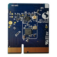
Dialog Semiconductor DA14580 User Manual (56 pages)
Ranger Extender Reference Application
Brand:
Dialog Semiconductor
| Category:
Extender
| Size: 2 MB
Table of Contents
Contents
3
Table of Contents
3
1 Terms and Definitions
9
2 References
9
3 Introduction
10
4 System Overview
10
Features
10
General Description
11
Bluetooth Soc
12
Figure 4: DA14580 QFN40 Soc, Range Extender Ver.2 Module
13
RF Front End
14
Radio Front End Control Signals
15
Table 2: BLE_ DIAGCNTL_REG (0X40000050) Register Specification
16
Figure 7: Diagnostic Port to Pins Assignment and Register Settings
17
Suggested Pin Assignment
18
Figure 8: the RF Control Signals
19
Power Amplifier
20
Low Pass Filter
21
Antenna
22
Range Extender V.2 on Interposer
22
Figure 15: Antenna Geometry on Range Extender V.2
23
Figure 17: Radiation Diagram for the Board Placed Vertically on the Short Edge
24
Range Extender V.2 Stand Alone
25
Figure 21: Radiation Diagram for the Board Placed Horizontally
26
Power System and Requirements
27
Trimming the 16Mhz Xtal
27
Pcba
28
Figure 25: Schematic of DA14580 Range Extender V.2 Module
29
September
30
Development Mode-Peripheral Pin Mapping
31
Figure 26: DA14580/581/583 Configuration Settings for Peripherals, Periph_Setup.h
32
Software
33
Figure 29: Step 3B of Adding App_Range_Extender
34
Figure 31: Step 4B of Adding App_Range_Extender
35
Figure 33: Step 5B of Adding App_Range_Extender
36
Figure 34: Inserting App_Range_Extender in the Production Test Tool
37
5 Measurements
38
Basic Performance Measurements
38
Receiver Sensitivity (Conducted)
38
Test Description
38
Test Results
38
Test Setup
38
Table 11: Conducted Rx Sensitivity
39
Test Description
40
Test Results
40
Test Setup
40
Transmitter Output Power (Conducted)
40
Figure 36: Peak Conducted Output Power Per Channel
41
Advertisement Mode
42
Current Consumption
42
Test Setup
42
Connection Mode
43
Extended Sleep Mode
44
FCC/ ETSI Measurements
45
Emission Limitation Conducted (Transmitter)
45
Emission Limitation Radiated (Transmitter)
45
Test Description
45
Test Results
45
Test Setup
45
Um-B
45
Test Results
46
Figure 41: FCC, Frequency Range from 30Mhz to 1 Ghz, CH39
47
Figure 43: FCC, Frequency from 1Ghz to 3Ghz, CH19
48
Figure 45: FCC, Frequency from 3Ghz to 18Ghz, CH00
49
Figure 47: FCC, Frequency from 3Ghz to 18Ghz, CH39
50
Figure 49: FCC, Frequency Range 2.31 Ghz to 2.39 Ghz (Restricted Band- CH19)
51
Figure 51: FCC, Frequency Range 2.4385 Ghz to 2.5 Ghz (Restricted Band- CH00)
52
6 FCC/IC Certification and CE Marking
53
Standards and Conformity Assessment
53
FCC Requirements Regarding the End Product and End User
53
End Product Marking
53
End Product Literature
53
Permissive Changes
53
Industry Canada Requirements Regarding the End Product and End User
53
Figure 54: Range Extender V.2 Module with External SPI Flash
54
7 Appendix A: Range Extender V.2 with SPI Data Flash
55
7 Appendix A: Range Extender V.2 with SPI Data Flash
55
8 Revision History
55
Advertisement
Related Products
Dialog Semiconductor DA1458 Series
Dialog Semiconductor SmartBond DA14585
Dialog Semiconductor DA14583
Dialog Semiconductor DA14581
Dialog Semiconductor DA14586
Dialog Semiconductor DA14531 PRO
Dialog Semiconductor DA14530/1
Dialog Semiconductor DA14695 USB Kit
Dialog Semiconductor DA14683
Dialog Semiconductor DA1469 PRO series
Dialog Semiconductor Categories
Microcontrollers
Motherboard
Network Hardware
Controller
Accessories
More Dialog Semiconductor Manuals
Login
Sign In
OR
Sign in with Facebook
Sign in with Google
Upload manual
Upload from disk
Upload from URL