Sign In
Upload
Manuals
Brands
Dialog Semiconductor Manuals
Microcontrollers
DA14530/1
Dialog Semiconductor DA14530/1 Manuals
Manuals and User Guides for Dialog Semiconductor DA14530/1. We have
1
Dialog Semiconductor DA14530/1 manual available for free PDF download: Hardware User Manual
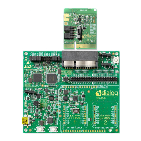
Dialog Semiconductor DA14530/1 Hardware User Manual (82 pages)
Development Kit Pro
Brand:
Dialog Semiconductor
| Category:
Microcontrollers
| Size: 7 MB
Table of Contents
Abstract
1
Table of Contents
2
Contents
2
Figures
4
Tables
5
Terms and Definitions
7
References
7
Introduction
8
Figure 1:DK PRO, DA14531-00FXDEVKT-P DK with PRO-MB and the PRO-Dbs
8
Table 1: DK PRO Part Numbers and Description
9
System Overview
10
Features of DA14531 PRO-DB
10
Features of DA14531 PRO-MB
10
Figure 2: Block Diagram of the DA14531 DK PRO Hardware Platform
10
Getting to Know DA14531 DK PRO
11
Da14531 Pro-Db
11
Figure 3: System Block Diagram of DA14531 PRO-DB
11
Figure 4: DA14531-00FXDB-P, FCGQFN24 PRO-DB_[376-04-F]
11
Figure 5: DA14531-00OGDB-P, WLCSP17 PRO-DB_[376-05-E]
12
Power Section
13
Figure 6: DA14531 PRO-DB Power Section
13
Figure 7: Power Section of DA14531 PRO-DB
14
RF Section
15
Figure 8: RF Section of DA14531 PRO-DB
15
Figure 9: Modifications Required for Performing RF Measurements
15
Pro-Mb (376-18-B)
16
Figure 10: Da145Xx DEVKT-P PRO-MB Block Diagram
16
Figure 11: PRO-MB (376-18-X)
16
Usb Hub (U11)
18
USB to UART (U12)
18
Figure 12: USB HUB Circuitry of DA14531 PRO-MB
18
USB to JTAG (U4)
19
Figure 13: USB to UART (U12)
19
Voltage Translator
20
Figure 14: USB to JTAG (U4)
20
Figure 15: Voltage Translator Circuitry of DA14531 PRO-MB
20
4.2.5 Power Section
21
Figure 16: Power Topology for DA14531 PRO-MB and PRO-DB
21
Figure 17: Power Circuit for DA14531 PRO-MB
21
Gpios and Pin Assignment and Functions of DA14531 DK PRO
22
Figure 18: J2, Breakout Header of DA14531 PRO-MB
22
Figure 19: J1, Configuration Header on DA14531 PRO-MB
23
(Default)
23
Table 2: PRO-MB to DA14531 Signal Correspondence and Function Multiplexing
23
DA14531 WLCSP17 PRO-DB, Default Setup
24
DA14531 FCGQFN24 PRO-DB, Default Setup
25
Table 3: DA14531 WLCSP Signals Assignment
25
Table 4: DA14531 FCGQFN24 PRO-DB and PRO-MB Signals Assignment (Default)
26
PRO-MB Setup
27
Reset
27
Figure 20: RESET Circuit on DA14531 PRO-MB
27
Figure 21: Reset Pin Assignment on PRO-Dbs for FCGQFN24 and WLCSP17
27
Jtag
28
SPI Data Flash (U2)
28
Figure 22: Optional Debug Port
28
Table 5: Configuration Settings for JTAG in DA14531 DK Pro
28
Table 6: Configuration Settings for SPI Data Flash in DA14531 DK Pro
28
Uart
29
Figure 23: SPI Data Flash Circuit in DA14531 DK Pro
29
Table 7: UART Signals Assignment in DA14531 DK PRO
29
Single-Wire UART
30
2-Wire UART Configuration
30
Figure 24: Single-Wire UART for DA14531 WLCSP17 PRO-DB
30
Table 8: Single-Wire UART Pin Assignment
30
Full UART (4-Wire) Configuration
31
Figure 25: 2-Wire UART Connectivity
31
Table 9: 2-Wire UART Pin Assignment
31
Table 10: Full UART Pin Assignment
31
Push Buttons
32
Figure 26: Full UART (4-Wire) Connectivity
32
Figure 27: Miscellaneous Peripherals
32
User LED (D5) and C-Trig (Software Cursor)
33
Figure 28: User LED and Software Trigger Circuit and Jumpers
33
Table 11: Configuration Settings for Push Buttons
33
Table 12: Configuration Settings for Miscellaneous Peripherals
33
Mikrobus 2 Interface
34
Figure 29: Mikrobus 2 Circuit
34
Table 13: Mikrobus 2 Signals
34
Arduino Interface
35
Table 14: Arduino Signals
35
How to Configure Power of DA14531 DK PRO
36
Figure 30: DA14531 PRO-DB Configuration and DA14531 PRO-MB Jumpers
36
Battery Operation
37
Table 15: DA14531 DCDC Configuration and Input Voltage
37
Table 16: Jumper Settings for J9
37
Enabling Coin Cell Battery on DA14531 PRO-DB
38
Enabling Coin Cell Battery on PRO-MB
38
Figure 31: BT1 Position (Left). Battery Holder, BC2032-F1, to be Soldered (Right)
38
Figure 32: DA14531 PRO-DB Schematic (Left). DA14531 PRO-MB, Header J4 Settings (Right)
38
Figure 33: BT1 Position on PRO-MB (Left). Battery Holder, BU2032SM-BT-GTR, to be Soldered (Right)
39
First Steps with DA14531 DK PRO
40
Configuration of DA14531 DK PRO with a DA14531 FCGQFN24 PRO-DB
40
Figure 34: Default Setup of the DA14531 DK PRO with DA14531 FCGQFN24 PRO-DB
40
Configuration of DA14531 DK PRO with a DA14531 WLCSP17 PRO-DB
42
Figure 35: Default Setup of the DA14531 DK PRO with a DA14531 WLCSP17 PRO-DB
42
Current Measurements
43
Current Measurement Circuit of PRO-MB
43
Figure 36: Current Measurement Circuit of DA14531 PRO-MB
43
Power Profiler of Smartsnippet Toolbox
44
Figure 37: Current Measurement Presented in Power Profiler of Smartsnippets Toolbox
44
Power Profiler Setup
45
Figure 38: Smartsnippets Toolbox Configuration
45
Figure 39: Hybrid Configuration
45
Figure 40: Power Profiler of Smartsnippets Toolbox Main Window
46
Figure 41: Power Profiler Configuration
46
Measurements
47
Figure 42: Power Profiler Chart Settings
47
Figure 43: Free Running Capture
47
Figure 44: Triggered Capture
48
Figure 45: Oscilloscope Option
48
Power Profiler Software Cursors
49
Manual Calibration
49
Figure 46: Power Profiler Software Cursors
49
Figure 47: Setting Offset to Zero
49
Figure 48: Measuring Offset
50
Figure 49: Setting Calibration Offset
50
Accuracy of Current Measurement Circuit
51
Figure 50: Current Measurement Circuit Response, Indicative Graph
51
Table 17: Accuracy of the Current Measurement Circuit
51
Figure 51: Current Measurement Circuit Inaccuracy, Indicative Graph
52
Known Issues
53
Switching Transient Artifacts of Current Measurement Circuit
53
Push Button SW3
53
Figure 52: A/D Converter Distortions
53
Figure 53: Disable SW3. Remove Jumper from J19:4-5
53
Mikrobus Wrong Labels
54
4-Wire UART Special Considerations
54
Figure 54: Mikrobus Wrong Label
54
Figure 55: Full UART Configuration - CTS Issue
55
Appendix A FCGQFN24 PRO-DB: DA14531-00FXDB-P_(376-04-F2)
56
Schematic
56
Figure 56: Schematic, FCGQFN24, DA14531-00FXDB-P_(376-04-F2)
56
Components Placement
57
Figure 57: Components on Top and Bottom Sides for FCGQFN24, DA14531-00FXDB-P_(376-04-F2)
57
Appendix B WLCSP17 PRO-DB: DA14531-00OGDB-P_(376-05-E)
58
Schematic
58
Figure 58: Schematic, WLCSP17, DA14531-00OGDB-P_(376-05-E)
58
Components Placement
59
Appendix C PRO-MB
60
Schematic
60
Figure 60: DA14531 PRO-MB, Headers and Connectors
60
Figure 61: DA14531 PRO-MB, Current Measurement Circuit
61
Figure 62: DA14531 PRO-MB, JTAG MCU
62
Figure 63: DA14531 PRO-MB, USB Hub, USB to UART IC, and Power Section
63
Components Placement
64
Figure 64: Components on Top Side of DA14531 PRO-MB
64
Appendix D Detailed Description of Hardware Setup
65
DA14531 WLCSP17 PRO-DB, Gpios Configuration, and R-Matrix
65
Figure 65: System Configuration for DA14531 DK PRO with a DA14531 WLCSP17 PRO-DB (Default)
65
Figure 67: System Configuration for DA14531 DK PRO with a DA14531 WLCSP17 PRO-DB
65
DA14531 FCGQFN24 PRO-DB, Gpios Configuration, and R-Matrix
66
Table 18: DA4531 WLCSP17 PRO-DB Default Setup
66
Figure 66: System Configuration for DA14531 DK PRO with a DA14531 FCGQFN24 PRO-DB (Default)
67
Table 19: DA4531 FCGQFN24 PRO-DB Default Setup
68
Appendix E SPI Data Flash, JTAG, and Single-Wire UART (Default)
69
DA14531 WLCSP17 PRO-DB and PRO-MB Settings
69
Table 20: Pin Assignment for DA14531 WLCSP17 PRO-DB
69
Table 21: Pin Assignment for DA14531 FCGQFN24 PRO-DB
69
Figure 68: Jumper Settings for PRO-MB (Marked in Red)
70
Table 22: the Components for DA14531 DK PRO in WLCSP17 Package
70
DA14531 FCGQFN24 PRO-DB and PRO-MB Settings
71
Figure 69: Resistor and Jumper Settings for DA14531 WLCSP17 PRO-DB
71
Figure 70: System Configuration for DA14531 DK PRO with a DA14531 FCGQFN24 PRO-DB (Default)
72
Figure 71: Jumper Settings for PRO-MB
73
Table 23: the Components for DA14531 DK PRO in FCGQFN24 Package
73
Figure 72: Resistor and Jumper Settings for DA14531 FCGQFN24 PRO-DB
74
Appendix F Enabling UART, JTAG and 32.768 Khz Crystal
75
UART (2-Wire), JTAG, and 32.768 Khz Crystal
75
Table 24: Pin Assignment for DA14531 WLCSP17 PRO-DB
75
Table 25: Pin Assignment for DA14531 FCGQFN24 PRO-DB
75
Table 26: the Components for the Two Packages to Support 2-Wire UART, JTAG, and 32.768 Khz Crystal
75
Figure 73: Resistor and Jumper Setting for PRO-MB (Top) and DA14531 PRO-Dbs (Bottom) to Support 2-Wire UART, JTAG, and 32.768 Khz Crystal
76
Full UART and JTAG
77
Table 27: Pin Assignment for DA14531 WLCSP17 PRO-DB
77
Table 28: Pin Assignment for DA14531 FCGQFN24 PRO-DB
77
Table 29: the Components for the Two Packages to Support Full UART and JTAG
77
Figure 74: Resistor and Jumper Setting for PRO-MB (Top) and DA14531 PRO-Dbs (Bottom) to Support Full UART and JTAG
78
Appendix G Operating the DK PRO at 1.5V (Boost Mode)
79
Adding External Resistor to VLDO Selection (J5) Pin Header
79
Using External Power Supply
79
Important Notice for Boost Operation
79
Figure 75: Configuring VLDO for 1.5V Boost Operation
79
Figure 76: Using External Power Supply for 1.5V Boost Operation
79
Figure 77: Examples of SPI Flash Power Management Using (Top) Analog Switch (Bottom) Directly
80
Revision History
81
Advertisement
Advertisement
Related Products
Dialog Semiconductor DA14580
Dialog Semiconductor DA1458 Series
Dialog Semiconductor SmartBond DA14585
Dialog Semiconductor DA14583
Dialog Semiconductor DA14581
Dialog Semiconductor DA14586
Dialog Semiconductor DA14531 PRO
Dialog Semiconductor DA14695-00HQDB-P
Dialog Semiconductor DA1468 series
Dialog Semiconductor DA1469 PRO series
Dialog Semiconductor Categories
Microcontrollers
Motherboard
Network Hardware
Accessories
Extender
More Dialog Semiconductor Manuals
Login
Sign In
OR
Sign in with Facebook
Sign in with Google
Upload manual
Upload from disk
Upload from URL