Sign In
Upload
Manuals
Brands
Abov Manuals
Microcontrollers
A96G174
Abov A96G174 Manuals
Manuals and User Guides for Abov A96G174. We have
1
Abov A96G174 manual available for free PDF download: User Manual
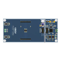
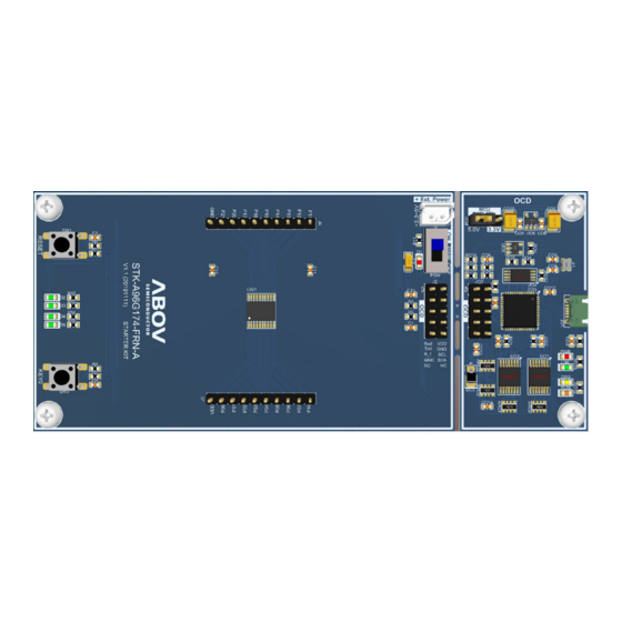
Abov A96G174 User Manual (211 pages)
16 MHz 8-bit A96G174 Microcontroller 8 Kbyte Flash memory, 12-bit ADC, 3 Timers, USART, I2C, Window WDT
Brand:
Abov
| Category:
Microcontrollers
| Size: 2 MB
Table of Contents
Introduction
1
Reference Document
1
Table of Contents
2
Description
11
Device Overview
11
Table 1. A96G174/A96S174 Device Features and Peripheral Counts
11
Table 1. A96G174/A96S174 Device Features and Peripheral Counts (Continued)
12
A96G174/A96S174 Block Diagram
13
Figure 1. A96G174/A96S174 Block Diagram
13
Pinouts and Pin Description
14
Pinouts
14
Figure 2. A96G174 20TSSOP Pin Assignment
14
Figure 3. A96S174 20TSSOP Pin Assignment
15
Figure 4. A96G174 20SOP Pin Assignment
16
Figure 5. A96G174 20QFN Pin Assignment
17
Figure 6. A96S174 20QFN Pin Assignment
18
Figure 7. A94G174 16SOPN Pin Assignment
19
Pin Description
20
Table 2. Normal Pin Description
20
Table 2. Normal Pin Description (Continued)
21
Table 2. Normal Pin Description (Continued)
22
Port Structures
23
Figure 8. General Purpose I/O Port
23
Figure 9. External Interrupt I/O Port
24
Central Processing Unit(CPU)
25
Architecture and Registers
25
Figure 10. M8051EW Architecture
25
Addressing
27
Instruction Set
28
Memory Organization
30
Program Memory
30
Data Memory
31
Figure 11. Program Memory Map
31
Figure 12. Data Memory Map
32
Figure 13. Lower 128Bytes of RAM
33
External Data Memory
34
Figure 14. XDATA Memory Area
34
SFR Map
35
SFR Map Summary
35
Table 3. SFR Map Summary
35
Table 4. XSFR Map Summary
36
SFR Map
37
Table 5. SFR Map
37
Table 5. SFR Map (Continued)
38
Table 5. SFR Map (Continued)
39
Table 6. XSFR Map
40
Compiler Compatible SFR
41
6 I/O Ports
43
Port Register
43
Data Register (Px)
43
Direction Register (Pxio)
43
Pull-Up Register Selection Register (Pxpu)
43
Open-Drain Selection Register (Pxod)
43
Bounce Enable Register (Pxdb)
43
Port Function Selection Register (Pxfsr)
43
Register Map
44
Table 7. Port Register Map
44
P0 Port
45
P0 Port Description
45
Register Description for P0
45
P1 Port
49
P1 Port Description
49
Register Description for P1
49
P2 Port
53
P2 Port Description
53
Register Description for P2
53
Interrupt Controller
55
External Interrupt
56
Figure 15. Interrupt Group Priority Level
56
Figure 16. External Interrupt Description
56
Pin Change Interrupt
57
Figure 17. Pin Change Interrupt
57
Block Diagram
58
Figure 18. Interrupt Controller Block Diagram
58
Interrupt Vector Table
59
Table 8. Interrupt Vector Address Table
59
Interrupt Sequence
60
Figure 19. Interrupt Sequence Flow
60
Effective Timing after Controlling Interrupt Bit
61
Figure 20. Effective Timing of Interrupt Enable Register
61
Figure 21. Effective Timing of Interrupt Flag Register
61
Multi-Interrupt
62
Figure 22. Effective Timing of Multi-Interrupt
62
Interrupt Enable Accept Timing
63
Interrupt Service Routine Address
63
Saving/Restore General Purpose Registers
63
Figure 23. Interrupt Response Timing Diagram
63
Figure 24. Correspondence between Vector Table Address and the Entry Address of ISR
63
Figure 25. Saving/Restore Process Diagram and Sample Source
63
Interrupt Timing
64
Interrupt Register Overview
64
Interrupt Enable Register (IE, IE1, and IE2)
64
Interrupt Priority Register (IP and IP1)
64
Figure 26. Timing Chart of Interrupt Acceptance and Interrupt Return Instruction
64
External Interrupt Flag Register (EIFLAG0 and EIFLAG1)
65
External Interrupt Polarity Register (EIPOL0L, EIPOL0H, and EIPOL1)
65
Register Map
65
Table 9. Interrupt Register Map
65
Interrupt Register Description
66
Clock Generator
69
Clock Generator Block Diagram
69
Figure 27. Clock Generator Block Diagram
69
Register Map
70
Register Description
70
Table 10. Clock Generator Register Map
70
Basic Interval Timer
71
BIT Block Diagram
71
BIT Register Map
71
Figure 28. Basic Interval Timer Block Diagram
71
Table 11. Basic Interval Timer Register Map
71
BIT Register Description
72
10 Watchdog Timer
73
Setting Window Open Period of Watchdog Timer
74
Figure 29. Watch Dog Timer Interrupt Timing Waveform
74
WDT Block Diagram
75
Register Map
75
Figure 30. Watch Dog Timer Block Diagram
75
Table 12. Watch Dog Timer Register Map
75
Table 13. Watchdog Timer Register Map
75
Register Description
76
Timer 0/1/2
78
Timer 0
78
8-Bit Timer/Counter Mode
78
Table 14. Timer 0 Operating Mode
78
Figure 31. 8-Bit Timer/Counter Mode for Timer 0
79
Figure 32. 8-Bit Timer/Counter 0 Example
79
8-Bit PWM Mode
80
Figure 33. 8-Bit PWM Mode for Timer 0
80
Figure 34. PWM Output Waveforms in PWM Mode for Timer 0
81
8-Bit Capture Mode
82
Figure 35. 8-Bit Capture Mode for Timer 0
82
Figure 36. Input Capture Mode Operation for Timer 0
83
Figure 37. Express Timer Overflow in Capture Mode
83
Timer 0 Block Diagram
84
Register Map
84
Figure 38. 8-Bit Timer 0 Block Diagram
84
Table 15. Timer 0 Register Map
84
Register Description
85
Timer 1
87
16-Bit Timer/Counter Mode
87
Table 16. TIMER 1 Operating Modes
87
Figure 39. 16-Bit Timer/Counter Mode of Timer 1
88
Figure 40. 16-Bit Timer/Counter Mode Operation Example
88
16-Bit Capture Mode
89
Figure 41. 16-Bit Capture Mode of Timer 1
89
Figure 42. Input Capture Mode Operation for Timer1
90
Figure 43. Express Timer Overflow in Capture Mode
90
16-Bit PPG Mode
91
Figure 44. 16-Bit PPG Mode of Timer 1
91
Figure 45. 16-Bit PPG Mode Operation Example
92
16-Bit Complementary PWM Mode (Dead Time)
93
Figure 46. 16-Bit Complementary PWM Mode for Timer1
93
Figure 47. 16-Bit Complementary PWM Mode Timing Chart for Timer 1
94
16-Bit Timer 1 Block Diagram
95
Register Map
95
Figure 48. 16-Bit Timer 1 Block Diagram
95
Table 17. TIMER 1 Register Map
95
Register Description
96
Timer 2
99
16-Bit Timer/Counter Mode
99
Table 18. TIMER 2 Operating Modes
99
Figure 49. 16-Bit Timer/Counter Mode of Timer 2
100
Figure 50. 16-Bit Timer/Counter Mode Operation Example
100
16-Bit Capture Mode
101
Figure 51. 16-Bit Capture Mode of Timer 2
101
Figure 52. 16-Bit Capture Mode Operation Example
102
Figure 53. Express Timer Overflow in Capture Mode
102
16-Bit PPG Mode
103
Figure 54. 16-Bit PPG Mode of Timer 2
103
Figure 55. 16-Bit PPG Mode Operation Example
104
16-Bit Timer 2 Block Diagram
105
Register Map
105
Figure 56. 16-Bit Timer 2 Block Diagram
105
Table 19. TIMER 2 Register Map
105
Register Description
106
12 12-Bit ADC
108
Conversion Timing
108
Block Diagram
109
Figure 57. 12-Bit ADC Block Diagram
109
Figure 58. A/D Analog Input Pin with a Capacitor
109
ADC Operation
110
Figure 59. Control Registers and Align Bits
110
Register Map
111
Register Description
111
Figure 60. ADC Operation Flow Sequence
111
Table 20. ADC Register Map
111
13 I2C
114
Block Diagram
114
Figure 61. I 2 C Block Diagram
114
Bit Transfer
115
Start/ Repeated Start/ Stop
115
Figure 62. Bit Transfer on the I2C-Bus
115
Figure 63. START and STOP Condition
115
Data Transfer
116
Acknowledge
116
Figure 64. Data Transfer on the I2C-Bus
116
Synchronization/ Arbitration
117
Figure 65. Acknowledge on the I2C-Bus
117
Figure 66. Clock Synchronization During Arbitration Procedure
118
Figure 67. Arbitration Procedure of Two Masters
118
Block Operation
119
I2C Block Initialization Process
119
I2C Interrupt Service
120
Master Transmitter
121
Slave Receiver
123
Register Map
124
Table 21. Register Map
124
I2C Register Description
125
14 Usart
129
Block Diagram
130
Figure 68. USART Block Diagram
130
Clock Generation
131
Figure 69. Clock Generation Block Diagram
131
Table 22. Equations for Calculating Baud Rate Register Setting
131
External Clock (XCK)
132
Synchronous Mode Operation
132
Figure 70. Synchronous Mode XCK Timing
132
Data Format
133
Figure 71. a Frame Format
133
Parity Bit
134
USART Transmitter
134
Sending Tx Data
134
Transmitter Flag and Interrupt
134
Parity Generator
135
Disabling Transmitter
135
USART Receiver
135
Receiving Rx Data
135
Receiver Flag and Interrupt
136
Parity Checker
137
Disabling Receiver
137
Asynchronous Data Reception
137
Figure 72. Start Bit Sampling
137
Figure 73. Sampling of Data and Parity Bit
138
Figure 74. Stop Bit Sampling and Next Start Bit Sampling
138
SPI Mode
139
SPI Clock Formats and Timing
139
Table 23. CPOL Functionality
139
Figure 75. SPI Clock Formats When UCPHA = 0
140
Figure 76. SPI Clock Formats When UCPHA = 1
141
Receiver Time out (RTO)
142
Figure 77. Example for RTO in USART
142
Table 24. Example Condition of RTO
142
Register Map
143
Table 25. USART Register Map
143
Register Description
144
Baud Rate Settings (Example)
151
Table 26. Examples of UBAUD Settings for Commonly Used Oscillator Frequencies
151
0% Error Baud Rate
153
Figure 78. 0% Error Baud Rate Block Diagram
153
15 Power down Operation
154
Peripheral Operation in IDLE/ STOP Mode
154
Table 27. Peripheral Operation Status During Power-Down Mode
154
IDLE Mode
155
STOP Mode
155
Figure 79. IDLE Mode Release Timing by an External Interrupt
155
Released Operation of STOP Mode
156
Figure 80. STOP Mode Release Timing by External Interrupt
156
Figure 81. STOP Mode Release Flow
157
Register Map
158
Register Description
158
Table 28. Power-Down Operation Register Map
158
16 Reset
159
Reset Block Diagram
159
Figure 82. Reset Block Diagram
159
Table 29. Hardware Setting Values in Reset State
159
Power on Reset
160
Figure 83. Fast VDD Rising Time
160
Figure 84. Internal RESET Release Timing on Power-Up
160
Figure 85. Configuration Timing When Power-On
161
Figure 86. Boot Process Waveform
161
External RESETB Input
162
Table 30. Boot Process Description
162
Figure 87. Timing Diagram after RESET
163
Figure 88. Oscillator Generating Waveform Example
163
Low Voltage Reset Process
164
Figure 89. Block Diagram of LVR
164
Figure 90. Internal Reset at Power Fail Situation
164
LVI Block Diagram
165
Figure 91. Configuration Timing When LVR RESET
165
Figure 92. LVI Block Diagram
165
Register Map
166
Reset Operation Register Description
166
Table 31. Reset Operation Register Map
166
17 Memory Programming
168
Flash Control and Status Registers
168
Register Map
168
Table 32. Flash Control and Status Register Map
168
Register Description
169
Figure 93. Read Device Internal Checksum (Full Size)
173
Figure 94. Read Device Internal Checksum (User Define Size)
174
Table 33. Program and Erase Time
175
Memory Map
176
Flash Memory Map
176
Figure 95. Flash Memory Map
176
Figure 96. Address Configuration of Flash Memory
176
Serial In-System Program Mode
177
Flash Operation
177
Figure 97. the Sequence of Page Program and Erase of Flash Memory
177
Figure 98. the Sequence of Bulk Erase of Flash Memory
178
Mode Entrance Method of ISP Mode
182
Mode Entrance Method for ISP
182
Figure 99. ISP Mode
182
Table 34. Operation Mode
182
Table 35. Mode Entrance Method for ISP
182
Security
183
Configure Option
183
Table 36. Security Policy Using Lock Bits
183
How to Write the Configure Option in User Program
184
18 Development Tools
185
Compiler
185
Core and Debug Tool Information
185
Table 37. Information of Core and Debug Emulation Interfaces
185
Feature of 94/96/97 Series Core
186
Table 38. Core and Debug Interface by Series
186
Table 39. Feature Comparison Chart by Series and Cores
186
OCD Type of 94/96/97 Series Core
188
Table 40. OCD Type of each Series
188
Table 41. Comparison of OCD 1 and OCD 2
188
Interrupt Priority of 94/96/97 Series Core
189
Table 42. Interrupt Priorities in Groups and Levels
189
Extended Stack Pointer of 94/96/97 Series Core
190
Figure 100. Configuration of the Extended Stack Pointer
190
OCD (On-Chip Debugger) Emulator and Debugger
191
Table 43. Debug Feature by Series
191
Figure 101. OCD 1 and OCD 2 Connector Pin Diagram
192
Table 44. OCD 1 and OCD 2 Pin Description
192
On-Chip Debug System
193
Figure 102. Debugger (OCD1/OCD2) and Pinouts
193
Table 45. OCD Features
193
Entering Debug Mode
194
Figure 103. On-Chip Debugging System in Block Diagram
194
Figure 104. Timing Diagram of Debug Mode Entry
194
Two-Wire Communication Protocol
195
Figure 105. 10-Bit Transmission Packet
196
Figure 106. Data Transfer on OCD
196
Figure 107. Bit Transfer on Serial Bus
197
Figure 108. Start and Stop Condition
197
Figure 109. Acknowledge on Serial Bus
198
Figure 110. Clock Synchronization During Wait Procedure
198
Programmers
199
OCD Emulator
199
Figure 111. E-PGM+ (Single Writer) and Pinouts
199
Gang Programmer
200
Flash Programming
200
On-Board Programming
200
Figure 112. E-Gang4 and E-Gang6 (for Mass Production)
200
Table 46. Pins for Flash Programming
200
Connection of Transmission
201
Figure 113. Connection of Transmission
201
Circuit Design Guide
202
Figure 114. PCB Design Guide for On-Board Programming
203
Appendix
204
Instruction Table
204
Table 47. Instruction Table
204
Table 47. Instruction Table (Continued)
205
Table 47. Instruction Table (Continued)
206
Table 47. Instruction Table (Continued)
207
Table 47. Instruction Table (Continued)
208
Revision History
209
Advertisement
Advertisement
Related Products
Abov A96G140
Abov A96G148
Abov A96T418GDN
Abov A96A148
Abov A96S174
Abov A96G150
Abov A96L414
Abov A96L416
Abov A31G31 Series
Abov A34M420
Abov Categories
Microcontrollers
Computer Hardware
Motherboard
Smoke Alarm
Control Unit
More Abov Manuals
Login
Sign In
OR
Sign in with Facebook
Sign in with Google
Upload manual
Upload from disk
Upload from URL