Advertisement
Table of Contents
- 1 Table of Contents
- 2 Technical Specifications
- 3 Warnings and Servicing Hints
- 4 Mechanical Instructions
- 5 Electrical and Circuit Diagrams
- 6 Diagnostic Software
- 7 Faultfinding Trees
- 8 Faultfinding Guide
- 9 Faultfinding Guide
- 10 List of Addreviations
- 11 Electrical Parts List
- 12 Power Supply Unit
- Download this manual
See also:
User Manual
Service
Manual
OPEN/CLOSE
REMARK : This service manual explains them by extracting specifications
designed for the model DR4050 only. The explanation for CD-R module
(Loader : CDL4009' + CD-R Main board) is not mentioned on this service
manual.
The CD-R module information is described in the service manual of CD-R
modules < 2nd line Service Manual : 3104 125 40110 >.
1.
TECHNICAL SPECIFICATIONS ............................................................................. 1
2.
WARNINGS AND SERVICING HINTS ................................................................... 2
3.
MECHANICAL INSTRUCTIONS ............................................................................. 5
4.
ELECTRICAL AND CIRCUIT DIAGRAMS ............................................................ 10
5.
DIAGNOSTIC SOFTWARE .................................................................................. 25
6.
FAULTFINDING TREES ....................................................................................... 29
7.
FAULTFINDING GUIDE ........................................................................................ 35
8.
LIST OF ADDREVIATIONS ................................................................................... 51
9.
ELECTRICAL PARTS LIST ................................................................................... 57
Please use this service manual with referring to the user guide (D.F.U) without fail.
Printed in Japan
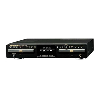
CD RECORDER DR4050
PLAY/PAUSE
STOP
REC TYPE
REC
FINALIZE
ERASE
SOURCE
CD-R
ON/OFF
STANDBY
PROG
SHUFFLE
TABLE OF CONTENTS
DR4050
DR4050/
EASY JOG
-
+
STORE
CANCEL
PLAY/PAUSE
/MENU
/DELETE
CD
PUSH ENTER
DISPLAY
SCROLL
REPEAT
DJ MODE
F1N, /N1G, /N1B, /U1B
CD Recorder
STOP
OPEN/CLOSE
PHONES
435W855010 AO
3120 785 22470
First Issue:2000.12
Advertisement
Table of Contents

Related Manuals for Marantz DR4050


Summary of Contents for Marantz DR4050
-
Page 1: Table Of Contents
REPEAT DJ MODE REMARK : This service manual explains them by extracting specifications designed for the model DR4050 only. The explanation for CD-R module (Loader : CDL4009’ + CD-R Main board) is not mentioned on this service manual. The CD-R module information is described in the service manual of CD-R modules <... - Page 2 MARANTZ Parts for your equipment are generally available to our National Marantz Subsidiary or Agent. ORDERING PARTS : Parts can be ordered either by mail or by Fax.. In both cases, the correct part number has to be specified.
-
Page 3: Technical Specifications
GB 1 1. Technical Specifications General Frequency range F.R. : 20Hz < F.R.< 20kHz Amplitude linearity 0.3dB (typical 0.1dB) Mains voltage : 220 - 240V/60Hz (/N1B,/N1G) : 100V/50-60Hz (/F1N) Channel unbalance : < 0.3dB at 1kHz (typical 0.2dB) : 120V/60Hz (/U1B) Output resistance : 200... -
Page 4: Warnings And Servicing Hints
GB 2 2. Warnings and Servicing Hints WARNING WAARSCHUWING All ICs and many other semi-conductors are Alle IC's en vele andere halfgeleiders zijn susceptible to electrostatic discharges (ESD). gevoelig voor elektrostatische ontladingen Careless handling during repair can reduce (ESD). life drastically. Onzorgvuldig behandelen tijdens reparatie When repairing, make sure that you are kan de levensduur drastisch doen... - Page 5 GB 3 SERVICING HINTS In the set, chip components have been applied. For disassembly and assembly check the figure below.
- Page 6 GB 4...
-
Page 7: Mechanical Instructions
GB 5 3. Mechanical instructions Wiring diagram Pin 1 indicated by All Wires are 1/1, except flex 8001, 8005 and 8007 0101 8006 3104 157 1099 8001 (at conn. 1400 8002 8003 (at conn. F934 0206 of CDR main board) of CDR main board) VDC2 VFTD... - Page 8 GB 6 Wiri ng CD WIRING DIAGRAM CD LOADER VAL1250 CONNECTOR 1006 CONNECTOR 1002 Connection tray motor and tray switch HALL + HOMESW SGND TRAY+ TRAY- HALL- LOADER VAL1250 CONNECTOR 1001 Tray 1002 HOMESW switch UCOIL SGND To main board CDR 1208 10 VCOIL 11 WCOIL...
- Page 9 9965 000 07459 LENS IR (GOLD) 435W355110 007B 010B BLK 9965 000 07460 LENS IR (BLACK) 435W355010 012B 9965 000 07461 BADGE MARANTZ 185J251010 014B GLD 9965 000 07462 LABEL CDR (GOLD) 435W861110 014B BLK 9965 000 07463 LABEL CDR (BLACK)
- Page 10 GB 8 Exploded view CD EXPLODED VIEW CD LOADER VAL1250 CLAMPER ASSY SUSPENSION RACK SPRING CDM VAM1250 SCREW MOTORSPRING SCREW SUSPENSION RACK RUBBER SUB CHASSIS RUBBER SWITCH SUSPENSION RUBBER SUSPENSION PLUG POS. VERS. PART NO. PART NO. DESCRIPTION COLOR (PCS) (MJI) RUBBER TRAY GEARWHEEL...
- Page 11 GB 9 Dismantling DISMANTLING INSTRUCTIONS See exploded views for item numbers Cover 165 assembling Remove 7 screws 166 172, 2 at each side and 3 at rear side. disassembling Lift cover at rear side to remove. CDR module includes : CD out board 1002 I/O board 1004 Power supply unit 1003...
-
Page 12: Electrical And Circuit Diagrams
GB 10 4. Electrical and circuit diagrams Blockdiagram OVERALL BLOCK DIAGRAM CDR MAIN BOARD ON/OFF CDL 4009 1302 LOADER ASSY 7703 2 WIRES 7330 1500 CDM3800 0205 1330 FLASH 0206 HALL +12V 11 WIRES POWER SUPPLY DRIVE, HALL FEEDBACK MOTOR FLEX 11P DRIVER UNIT... - Page 13 GB 11 Display 0100 G10 F147 E3 1050 H7 F148 E7 1101 B9 F149 F3 1102 C12 F150 F7 1103 C11 F151 F7 DISPLAY BOARD LAYOUT .5 - CIRCUIT DIAGRAM 1104 C12 F152 F3 1105 B10 F153 F3 1106 B11 F154 F7 1107 B12 F155 G7...
- Page 14 GB 12 Display DISPLAY BOARD CDR775 LAYOUT.5 TOP VIEW PB DISPLAY 4230 3104 123 4230.5 DISPLAY BOARD CDR775 LAYOUT.5 BOTTOM VIEW PB DISPLAY 4230 3104 123 4230.5...
- Page 15 GB 13 R on/off IR BOARD CDR775 - CIRCUIT DIAGRAM IR BOARD - FRONT VIEW 1200 A1 6200 A3 F200 A2 F201 A2 F202 A2 F200 6200 1200 EH-S TSOP1736 F201 F202 IR BOARD - BACK VIEW TO DISPLAY BOARD GNDB PB DISPLAY - 4230 CDR 775...
- Page 16 GB 14 HPCD out HEADPHONE BOARD CDR775 - CIRCUIT DIAGRAM HEADPHONE BOARD - TOP VIEW 0400 A2 1400 A1 1401 A3 2400 A2 2401 B2 F400 A2 F401 A1 F402 B2 2400 1401 F400 GNDC 1400 HLJ1540 PH-B F401 0400 GNDC GND WIRE GNDC...
- Page 17 GB 15 I/O board I/O BOARD - CIRCUIT DIAGRAM 1000-1 F1 1000-10 C9 F100 3025 F101 +5VDS 1000-11 C9 +5VDS 1000-12 B9 1000-13 B1 3021 DRIVER 1000-14 C9 1000-2 E1 GP1F32T 1001-A 3024 1000-3 E1 5002 7010 YKC21-3421 1000-4 D9 BLM21 F102 F103...
- Page 18 GB 16 I/O board I/O BOARD - TOP VIEW I/O BOARD - BOTTOM VIEW...
- Page 19 GB 17 PSU 99 0101 A 1 0205 G15 0205 C15 0207 I16 1120 B 2 2106 K 2 2114 I 7 2129 E 5 2213 B15 2233 C15 2252 E15 3105 I 2 3111 F 6 3122 A 3 3128 D 9 3204 I11 3232 E13...
- Page 20 GB 18 PSU 99 POWER SUPPLY UNIT 20PS317 - COMPONENT SIDE 0101 D 0208 A 11 2120 C 2127 B 2213 B 11 2233 C 11 2251 B 3120 B 3126 B 3201 D 5120a A 5220 A 10 5250 C 10 6113 D 6220 A 6250 B...
- Page 21 GB 19 CD Diagram 1A 1000-1 C1 1000-7 H1 1020 G10 2148 C1 2159 D1 2169 F8 2183 F3 2232 H13 3164 B15 3178 C8 3187 D2 3196 E6 3205 E7 3219-C G13 3269 H14 3282 G11 7006 D3 7130 H15 F151 C13 F164 D7 F174 E7...
- Page 22 GB 20 CD diagram 1B 1000-13 E1 F100 F3 1000-14 E1 F101 F1 1000-15 D1 F102 A11 1000-16 D1 F103 A2 CD MAIN BOARD - CIRCUIT DIAGRAM 1B 1001 B1 F104 F4 1002 A1 F105 A11 1005 F5 F106 F1 SERVO DRIVERS PART 1006-1 F1 F107 A2...
- Page 23 GB 21 CD diagram 1C 1208-10 C11 F325 G10 1208-11 C11 F329 G10 1208-12 D11 F350 G7 1208-13 D11 F351 G7 CD MAIN BOARD - CIRCUIT DIAGRAM 1C 1208-14 A11 F352 G7 1208-2 B11 F353 H10 1208-22 D11 F354 I9 AUDIO PART 1208-3 G11 F355 I10...
- Page 24 GB 22 CD diagram 2 1205 F7 1206 D12 1207 E12 VPROC VPROC VPROC 3999 CD MAIN BOARD - CIRCUIT DIAGRAM 2 1208-1 E13 1208-15 E13 VPROC VPROC VPROC VPROC 1208-16 D13 MICROPROCESSOR PART 1208-17 E13 1208-18 I13 1208-19 H13 1208-20 I13 1208-21 I13 1208-7 G13...
- Page 25 GB 23 CD top CD MAIN BOARD - TOP VIEW...
- Page 26 GB 24 CD bottom CD MAIN BOARD - BOTTOM VIEW...
-
Page 27: Diagnostic Software
GB 25 5. Diagnostic Software Dealer mode 5.2.2 Requirements to perform the test Working keyboard to start up the test. The purpose of the dealer mode is to prevent people taking out Working local display to check the output messages. the CD inside the player at exhibitions, showrooms etc.. - Page 28 GB 26 Electrical service diagnostics ELECTRICAL SERVICE DIAGNOSTICS (software versions, test for defective components) If power ON, switch power OFF Load CD-DA disc (SBC444A) Press <PLAY> + <F FWD> simultaneously and switch ON unit LOADER TESTS PLAYER INFORMATION CDR LOADER TEST Display : ABORT TEST CD-DA disc must be loaded...
- Page 29 GB 27 5.3.1 Description disc test is executed to check focus control, disc motor control, radial control and jump grooves control. The disc test is performed by audio play-back of 5 seconds at the beginning, The intention of the electrical service diagnostics is to show the middle and end of the disc.
- Page 30 GB 28 5.4.2 Requirements to perform the test 5.5.1 Description Working keyboard to cycle through the tests and to start up This test is initiated by pressing [ERASE] and [RECORD] the test. simultaneously while switching on the unit. The player will Working local display to check the output messages.
-
Page 31: Faultfinding Trees
GB 29 6. Faultfinding trees CDR-Module NO DISC LOADED SWITCH ON POWER STBY LED? PRESS <DISPLAY> CHECK: MAINS, MAINS CABLE POWER SUPPLY (SEE FAULT FINDING GUIDE PSU) WIRING ON/OFF SWITCH FUSES VOLTAGES DISPLAY (SEE FAULT FINDING GUIDE DISPLAY BOARD) DISPLAY? WIRING SUPPLY VOLTAGES CLOCK SIGNAL 8MHz... - Page 32 GB 30 CD-DA DISC LOADED CHECK: WIRING POWER SUPPLY VOLTAGES DISC ELECTRICAL SERVICE DIAGNOSTICS: DETECTION & READING? REPLACE CDR MODULE IF "DERRn" OR "BERRn" ERROR OCCURS CHECK: DISC: DIRT, SCRATCHES, DAMAGED... DISPLAY: ELECTRICAL SERVICE DIAGNOSTICS: “CD” & REPLACE CDR MODULE IF "DERRn" T.O.C.
- Page 33 GB 31 CD-R DISC LOADED CHECK: DISC WIRING DETECTION & POWER SUPPLY VOLTAGES READING? ELECTRICAL SERVICE DIAGNOSTICS: REPLACE CDR MODULE IF "DERRn" OR "BERRn" ERROR OCCURS CHECK: DISPLAY: DISPLAY: DISC: DIRT, SCRATCHES, DAMAGED... “CD R” & “CD” & ELECTRICAL SERVICE DIAGNOSTICS: OPC INFO? T.O.C.
- Page 34 GB 32 CD-RW DISC LOADED CHECK: DISC WIRING DETECTION & POWER SUPPLY VOLTAGES READING? ELECTRICAL SERVICE DIAGNOSTICS: REPLACE CDR MODULE IF "DERRn" OR "BERRn" ERROR OCCURS CHECK: DISPLAY: DISPLAY: DISC: DIRT, SCRATCHES, DAMAGED... “CD RW” & “CD” & ELECTRICAL SERVICE DIAGNOSTICS: OPC INFO? T.O.C.
-
Page 35: Faultfinding Guide
GB 33 CD Module CD MODULE NO DISC POWER ON CHECK FLEX CONNECTION FROM CDR MAIN BOARD POWER SUPPLY +5V, +12V AT TESTPOINTS 28 AND 27 +5V AT CONN. 1000 PINS 1 AND 3 +5V AT IC7005 PIN 14 +3V3 AT IC7000 PINS 5,17,21,57, CHECK SAFETY RESISTORS DISC +5V AT IC7020 PIN 25 DETECTION... - Page 36 GB 34 CD MODULE PLAYBACK PRESS <PLAY> DAC 7309 TESTPOINTS 20, 21, 22 : I 2 S AT INPUT OF DAC 7309 CHECK POWER SUPPLY PINS 4, 13 CHECK CLK11 AT PIN 6 : 11.2896MHz AUDIO? PIN 11 : MUTE HIGH? TESTPOINTS 23, 24 : ANALOG OUTPUT? REPLACE DAC 7309 OPAMP 7120...
-
Page 37: Faultfinding Guide
GB 35 7. Faultfinding Guide Display Board Display controller TMP87C874F TMP87C874F (IC7104) is a high speed and high performance 8-bit single chip microprocessor, containing 8-bit A/D 7.1.1 Description of display board conversion inputs and a VFT (Vacuum Fluorescent Tube) driver. In this application, its functions are : General description slave microprocessor. - Page 38 GB 36 Grid lines 7.1.2 Test instructions Level and timing of all grid lines, G1-->G15, can be checked either at the FTD itself or at the display controller. Grid lines Supply voltages G13, G14 and G15 each have an extra current amplifier in line The display board receives several voltages via connector : T7203 for G13, T7204 for G14 and T7100 for G15.
- Page 39 GB 37 The pulses created this way arrive at pin 16 and 17 of the display controller. The first pulse to arrive tells the controller the PM3392A direction of the rotation. Counting the pulses reveals the amount of rotation. Combining and decoding this information, the display controller will execute the appropriate task.
- Page 40 GB 38 7.1.3 Display board troubleshooting guide SWITCH POWER ON, EXIT STAND BY MODE CHECK : SUPPLY VOLTAGES -38V 5% at conn. 1119-2 10% between conn. 1119-1 and 1119-3 DISPLAY? 5 % at conn. 1119-10 (1121-4 for CDR570/930) CLOCK SIGNAL 8Mhz at pins 8, 9 of IC7104 CONTROL SIGNALS RESETN 3V3 (high) at conn.1119-4 after start up...
- Page 41 GB 39 Power Supply Unit 20PS317 cycle is regulated so that the output voltages are independent of load or input voltage variations. The controlling device MC44603 is an integrated pulse width modulator. A clock 7.2.1 Description of PSU 20PS317 signal initiates power pulses at a fixed frequency. The termination of each output pulse occurs when a feedback MOSFET 7125 is used as a power switch controlled by the signal of the inductor current reaches a threshold set by the...
- Page 42 GB 40 Pin function description Name Description This pin is the positive supply of the IC. The operating voltage range after start-up is 9.0 to 14.5 V. The output high state (VOH) is set by the voltage applied to this pin. Output Peak currents up to 750 mA can be sourced or sunk, suitable for driving either MOSFET or bipolar transistors.
- Page 43 GB 41 Block diagram of MC44603 Vref Iref Vref DEMAGNETISATION enable DETECT DEMAGNETISATION REFERENCE SUPPLY UVL01 MANAGEMENT BLOCK INITIALISATION BLOCK Iref VOSC PROT VOSC SYNC INPUT OSCILLATOR 1Set BUFFER LATCH RF STANDBY Vstby 1Reset STANDBY RP STANDBY (REDUCED FREQUENCY) 2.5V THERMAL SHUTDOWN Vref...
- Page 44 GB 42 is switched off when the current sense level exceeds the level at the output of the error amplifier. TimeON phase : A drain current will flow from the positive CH1 2 supply at pin 2 of the transformer through the transformer's PM3394B CH3 2 V~ ALT MTB5.00us- 0.90dv ch1- primary winding, the MOSFET and Rsense to ground.
- Page 45 GB 43 Circuit description of PSU 20PS317 Demagnetisation The auxiliary winding (7-9) voltage is used to detect magnetic saturation of the transformer core and connected via R3101 to Input circuit pin 8 of IC7110. During the demagnetisation phase, the output The input circuit consists of a lightning protection circuit and an will be disabled.
- Page 46 GB 44 7.2.2 Troubleshooting PSU 20PS317 Check fuse 1120 and replace if necessary Check DC voltage Power supply unit OK +5V, +12V, -8V, VFTD (-38V), VDC1-VDC2 (3V8) Disconnect power supply unit from CDR main board Connect dummy load resistors 10W, 15 ohm at +5V, +12V and ground Check DC voltage Power supply is OK...
- Page 47 GB 45 Connect on pin 2 of position 1208 a clock signal of 8.4672 MHz ( 100ppm minimum rise time of 50ns and at TTL level CDM VAM1250 Loader assy (0V and +5V). HF ampl. Keep microprocessor 7202 in reset by forcing pin 7 at Trigenta Diode signals position 1208 to +5V.
- Page 48 GB 46 Pin Configuration Location Value DC 7022 5.8V 7022 5.8V SBSY 7022 5.8V HFREF SFSY 7022 5.8V HFIN 7021 5.8V ISLICE 7021 5.8V SSA1 7021 TRAY- 5.8V TEST3 DDA1 7021 TRAY+ 5.8V STATUS CL96532086_054.eps SILD 080999 SAA7324 Figure 7-25 RESET 7.3.5 BA6856FP Turn Table Motor Driver (7020)
- Page 49 GB 47 Motor controller truth table Input conditions conn 1006 pin Outputs conn 1006 Test points on driver UCOIL VCOIL WCOIL HALL_U HALL_V HALL_W CL96532086_055.eps 080999 Figure 7-26 Hall-elements input signal voltage levels Input voltage Level Tolerance Unit CL96532086_056.eps 080999 Figure 7-27 7.3.6 Tray Control...
- Page 50 GB 48 7.3.7 HF Path another amplification and filtering circuit. The filtering again is controlled by the S1 and S2 lines, dependant on whether the disc starts up (speed n=1, S1 and S2 Low), disc plays at speed Description n=1 (S1 Low, S2 High) or disc plays at speed n=2 (S1 and S2 The pre-amplified HF-signal is presented to both n=1 and n=2 High).
- Page 51 GB 49 Transfer Characteristics function generator as a sine wave generator with output level Set the power and reset connections as described above in of 1Vtt. Check this AC value with an AC mV-meter connected "1.1.1. Supply Voltages". Connect a function generator via a to the input (pin 2) of the CD10 (7000) : serial resistor of 1k5 to pin 4 of connector 1000.
- Page 52 GB 50 Measurements 1200 - 17 AMPLIFIER CLK11 1200 - 19 NMUTE CL96532086_062.eps 080999 Figure 7-33 Keep processor 7202 in reset by forcing pin 7 of connector 1208 to +5V. This puts the processor outputs in tristate. Check the reset at pin 4 of processor 7202 to make sure that the processor is in reset.
-
Page 53: List Of Addreviations
GB 51 8. List of Abbreviations SIGNAL NAME SIGNAL FLOW FUNCTION AND DESCRIPTION +12V main supply voltage from PSU +12V supply voltage from PSU +12VA supply voltage +12V supply voltage for Audio part main supply voltage from PSU +5V supply voltage from PSU +5VA supply voltage +5V supply voltage for Audio part... - Page 54 GB 52 CDR60MEAS1 IC7300 -> R3382A -> CONN1812 serial output of information about jitter, PLL frequency and asymmetry of bit recovery block in CDR60, to be measured at test connector CDR60PLL IC7270 -> R3305 -> IC7300 CDR60 clock multiplier enable, active high CDRW IC7355D ->...
- Page 55 GB 53 ERASEC IC7008 -> R3087 ERASE Current switch CDRW output ERON IC7008 -> IC 7010 ERror ON (to AEGER) EXT_DIG_IN1 CONN1400 -> IC7701 EXTernal DIGital INput 1 EXT_DIG_IN2 CONN1702, C2767, C2721 -> R3701 - EXTernal DIGital INput 2 (CDR950 only) >IC7701 EXT_OPT_IN CONN1400, C2722 ->...
- Page 56 GB 54 INT_COPY_AN IC7701 -> R3721 -> IC7401IC7701 -> select INTernal COPY ANAlog (in case of copy protected disc or track R3721 -> R3410 on CD drive) (CDR775 only) T7135 -> CONN1000T7135 -> laser Read drive current signal R3056T7135 -> IC7008 T7122 ->...
- Page 57 GB 55 PRCOARSE IC7016 -> R3057 drive signal from Power Read COARSE DAC for read current source PRFINE IC7016 -> R3058 drive signal from Power Read FINE DAC for read current source PROF_EBU IC7701 -> CONN1820 PROFessional digital output (CDR950 only) PSENn IC7270 ->...
- Page 58 GB 56 TRACE99_RXD CONN1818 -> R3838, IC7701 TRACE99 test tool receive data TRACE99_TXD IC7701 -> CONN1818 TRACE99 test tool transmit data TRAYIN IC7270 -> IC7240 move TRAY IN line, active low TRAYOUT IC7270 -> IC7240 move TRAY OUT line, active low TRAYSW CONN1200 ->...
-
Page 59: Electrical Parts List
GB 57 9. ELECTRICAL PARTS LIST NOTE ON SAFETY FOR FUSIBLE RESIST OR : ASSIGNMENT OF COMMON PARTS CODES. RESISTORS The suppliers and their type numbers of fusible resistors are as 1) GD05 x x x 140, Carbon film fixed resistor, 5% 1/4W follows ;... - Page 60 GB 58 VERS. PART NO. VERS. POS. POS. PART NO. PART NO. PART NO. DESCRIPTION DESCRIPTION COLOR (PCS) COLOR (PCS) (MJI) (MJI) I/O CIRCUIT BOARD 1114 4822 276 13114 SWITCH, PUSH BUTTON QP27613114 MISCELLANEOUS 1115 4822 276 13114 SWITCH, PUSH BUTTON QP27613114 1000 2422 025 16289 CON PRINTED 14P...
- Page 61 GB 59 VERS. PART NO. VERS. POS. POS. PART NO. PART NO. PART NO. DESCRIPTION DESCRIPTION COLOR (PCS) COLOR (PCS) (MJI) (MJI) 4010 4822 051 10008 0R00 5% 0.25W QP05110008 CAPACITORS 4011 4822 051 10008 0R00 5% 0.25W QP05110008 2100 4822 126 14585 CER.
- Page 62 GB 60 VERS. PART NO. VERS. POS. POS. PART NO. PART NO. PART NO. DESCRIPTION DESCRIPTION COLOR (PCS) COLOR (PCS) (MJI) (MJI) 2172 5322 126 10794 CER. 220pF 5% 63V QQ12610794 3130 4822 117 10833 10k 1% 0.1W QP11710833 2173 5322 126 10794 CER.
-
Page 63: Power Supply Unit
GB 61 VERS. VERS. POS. PART NO. POS. PART NO. PART NO. PART NO. DESCRIPTION DESCRIPTION COLOR (PCS) COLOR (PCS) (MJI) (MJI) 3226 4822 117 10833 10k 1% 0.1W QP11710833 7019 4822 130 60373 TRS. BC856B QP13060373 3229 4822 117 11748 2R2 5% 1206 FUSE QP11711748 7020... - Page 64 GB 62 VERS. PART NO. VERS. POS. POS. PART NO. PART NO. PART NO. DESCRIPTION DESCRIPTION COLOR (PCS) COLOR (PCS) (MJI) (MJI) 2234 4822 124 81151 ELECT 22 F 50V QP12481151 6210 4822 130 83865 DIODE SB360 QP13083865 2240 4822 124 40196 ELECT 220 F 20% 16V QP12440196 6220 4822 130 42488 DIODE BYD33D...
Need help?
Do you have a question about the DR4050 and is the answer not in the manual?
Questions and answers