Table of Contents
Advertisement
Service
Manual
UNIVERSAL MULTI-CD SYSTEM
CDX-FM653
- See the separate manual CX-892(CRT2356) for the CD mechanism description, disassembly and circuit
description.
- The CD mechanism employed in this model is one of C7 series.
CONTENTS
1. SAFETY INFORMATION ............................................2
2. EXPLODED VIEWS AND PARTS LIST .......................4
3. SCHEMATIC DIAGRAM ...........................................12
4. PCB CONNECTION DIAGRAM ................................24
5. ELECTRICAL PARTS LIST ........................................32
6. ADJUSTMENT..........................................................36
PIONEER ELECTRONIC CORPORATION
PIONEER ELECTRONICS SERVICE INC.
PIONEER ELECTRONIC [EUROPE] N.V.
PIONEER ELECTRONICS ASIACENTRE PTE.LTD. 253 Alexandra Road, #04-01, Singapore 159936
C PIONEER ELECTRONIC CORPORATION 1999
4-1, Meguro 1-Chome, Meguro-ku, Tokyo 153-8654, Japan
P.O.Box 1760, Long Beach, CA 90801-1760 U.S.A.
Haven 1087 Keetberglaan 1, 9120 Melsele, Belgium
7. GENERAL INFORMATION .......................................43
7.1 PARTS .................................................................43
7.1.1 IC................................................................43
7.1.2 DISPLAY ....................................................49
7.2 DIAGNOSIS ........................................................50
7.2.1 DISASSEMBLY .........................................50
7.2.2 TEST MODE ..............................................52
7.3 BLOCK DIAGRAM ..............................................58
8. OPERATIONS AND SPECIFICATIONS.....................60
K-ZZY. FEB. 1999 Printed in Japan
ORDER NO.
CRT2321
X1N/UC
Advertisement
Table of Contents

Related Manuals for Pioneer CDX-FM653


Summary of Contents for Pioneer CDX-FM653
-
Page 1: Table Of Contents
PIONEER ELECTRONICS SERVICE INC. P.O.Box 1760, Long Beach, CA 90801-1760 U.S.A. PIONEER ELECTRONIC [EUROPE] N.V. Haven 1087 Keetberglaan 1, 9120 Melsele, Belgium PIONEER ELECTRONICS ASIACENTRE PTE.LTD. 253 Alexandra Road, #04-01, Singapore 159936 C PIONEER ELECTRONIC CORPORATION 1999 K-ZZY. FEB. 1999 Printed in Japan... -
Page 2: Safety Information
CDX-FM653 - CD Player Service Precautions 3. Please checking the grating after changing the pick- 1. For pickup unit(CXX1285) handling, please refer up unit (See page 37). to"Disassembly"(See page 50). During replacement, 4 Since these screws protects the mechanism during... - Page 3 CDX-FM653...
-
Page 4: Exploded Views And Parts List
CDX-FM653 2. EXPLODED VIEWS AND PARTS LIST 2.1 PACKING... - Page 5 CDX-FM653 NOTE: - Parts marked by “*” are generally unavailable because they are not in our Master Spare Parts List. ∇ mark on the product are used for disassembly. - Screws adjacent to - PACKING SECTION PARTS LIST Mark No. Description Part No.
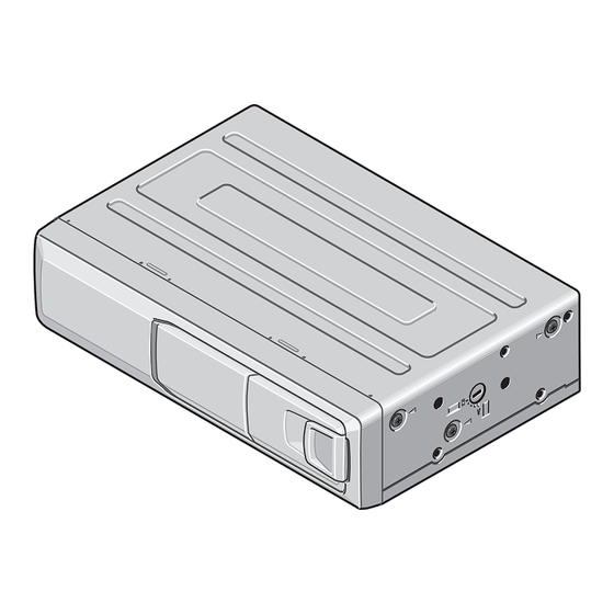
- Page 6 CDX-FM653 2.2 EXTERIOR...
- Page 7 CDX-FM653 - EXTERIOR SECTION PARTS LIST Mark No. Description Part No. Mark No. Description Part No. 1 Screw BMZ26P040FMC 36 Display Assy CXB3249 2 Screw BMZ30P040FZK 37 Screw BPZ20P100FZK 3 Button CAC4632 38 Button CAC5887 4 Screw CBA1460 39 Cord...
- Page 8 CDX-FM653 2.3 CD MECHANISM MODULE...
- Page 9 CDX-FM653 - CD MECHANISM MODULE SECTION PARTS LIST Mark No. Description Part No. Mark No. Description Part No. 1 Connector CDE6069 46 Spacer CNM6146 2 CD Core Unit (C7) CWX2279 47 Sheet CNM6296 3 Connector(CN701) CKS1963 48 PCB CNP5227 4 Connector(CN101)
- Page 10 CDX-FM653 Mark No. Description Part No. 91 Screw JGZ17P025FZK 92 Pickup Unit(Service) CXX1285 93 ••••• 94 ••••• 95 Screw IMS26P040FMC 96 Screw JFZ20P025FNI 97 Photo-transistor(Q851) PT4800 CSN1051 Spring Switch(S851,S853) 99 LED(D851) CN504-2 100 Spring Switch(S852) CSN1052...
- Page 11 CDX-FM653 2.4 MAGAZINE ASSY - MAGAZINE ASSY SECTION PARTS LIST Mark No. Description Part No. 1 Magazine Assy CXB4027 2 Label CRW1395 3 Tray CNV5341...
-
Page 12: Schematic Diagram
CDX-FM653 3. SCHEMATIC DIAGRAM 3.1 OVERALL CONNECTION DIAGRAM Note: When ordering service parts, be sure to refer to “EXPLODED VIEWS AND PARTS LIST” or “ELECTRICAL PARTS LIST”. PICKUP UNIT(SERVICE) MECHANISM CXX1285 RF-A M854 CXB3004 M851 CXB3003 CSN1051 PT4800 SWITCH PCB... - Page 13 CDX-FM653 CD CORE UNIT RF-AMP,SERVO, DSP,DAC 19 20 DRIVER MOTOR DRIVER A1/2...
- Page 14 CDX-FM653 LOUT AAGND ROUT SYSTEM CONTROLLER...
- Page 15 CDX-FM653 CN201...
- Page 16 CDX-FM653 Note:1. The encircled numbers denote measuring pointes in the circuit diagram. 2. Reference voltage REFO:2.5V - Waveforms 1 RFI 1 CH1: RFI 1 CH1: RFI 0.5V/div. 0.5µs/div. 1V/div. 1V/div. 0.5ms/div. 0.5ms/div. 2 CH2: MIRR 2 CH2: MIRR Normal mode: play 5V/div.
- Page 17 CDX-FM653 8 CH1: TE 8 CH1: TE 0 MD 0.2V/div. 0.5V/div. 0.5V/div. 0.1s/div. 20ms/div. 5ms/div. 9 CH2: TD ! CH2: SD 0.2V/div. 0.5V/div. Normal mode: play TEST mode:100Tracks jump(FWD) Normal mode: Play (12cm) → REFO → REFO → REFO →...
- Page 18 CDX-FM653 ( CH1: R OUT 8 CH1: TE 6 CH1: FE 2V/div. 0.2V/div. 0.2V/div. 1ms/div. 500µs/div. 1ms/div. ) CH2: L OUT 3 CH2: FD 9 CH2: TD 2V/div. 0.5V/div. 0.5V/div. Normal mode: Play (1kHz 0dB) Normal mode: During AGC Normal mode: During AGC →...
- Page 19 CDX-FM653...
- Page 20 CDX-FM653 3.2 EXTENSION UNIT 19kHz ADD ON MODE CN701 38KHz 7.2MHz LOOP FILTER 6V REG. 3V REG. CN901 5V REG. VD REGULATOR...
- Page 21 CDX-FM653 MPX AMP PILOT BUFFER AMP CN501 FUSE 2A CEK1018 1K(1/2W) EXTENSION UNIT...
- Page 22 CDX-FM653 3.3 ANTENNA SELECT UNIT...
- Page 23 CDX-FM653 3.4 DISPLAY ASSY...
-
Page 24: Pcb Connection Diagram
CDX-FM653 4. PCB CONNECTION DIAGRAM SIDE A 4.1 CD CORE UNIT M852 NOTE FOR PCB DIAGRAMS 1. The parts mounted on this PCB include all necessary parts for several destination. For further information for respective destinations, be sure to check with the schematic dia-... - Page 25 CDX-FM653 2. Viewpoint of PCB diagrams SIDE B Capacitor Connector SIDE A SIDE B P.C.Board Chip Part...
- Page 26 CDX-FM653 4.2 EXTENSION UNIT SIDE A CN701 EXETENSION UNIT CORD CN901 CN501...
- Page 27 CDX-FM653 SIDE B EXETENSION UNIT...
- Page 28 CDX-FM653 4.3 MECHANISM PCB MECHANISM PCB PICKUP UNIT M851 (SERVICE) SPDL HOME M854 CN101 4.4 SWITCH PCB SWITCH PCB D851...
- Page 29 CDX-FM653 4.5 MOTOR PCB MOTOR PCB 4.6 ANTENNA SELECT UNIT ANTENNA SELECT UNIT CN401 TUNER ANTENNA...
- Page 30 CDX-FM653 4.7 DISPLAY ASSY SIDE A...
- Page 31 CDX-FM653 SIDE B...
-
Page 32: Electrical Parts List
CDX-FM653 5. ELECTRICAL PARTS LIST NOTE: - Parts whose parts numbers are omitted are subject to being not supplied. - The part numbers shown below indicate chip components. Chip Resistor RS1/_S___J,RS1/__S___J Chip Capacitor (except for CQS..) CKS.., CCS.., CSZS..=====Circuit Symbol and No.===Part Name Part No. - Page 33 CDX-FM653 =====Circuit Symbol and No.===Part Name Part No. =====Circuit Symbol and No.===Part Name Part No. ------ ------------------------------------------ ------------------------- ------ ------------------------------------------ ------------------------- RS1/16S102J CKSQYB104K25 RS1/16S104J CSZST220M16 RS1/16S104J CKSRYB103K25 RS1/16S223J CKSRYB103K25 RS1/16S472J CKSRYB102K50 RA4C473J CKSRYB102K50 RA4C473J CKSRYB103K25 RS1/16S472J CKSRYB103K25 RS1/16S104J CKSRYB103K25 RS1/16S473J...
- Page 34 CDX-FM653 =====Circuit Symbol and No.===Part Name Part No. =====Circuit Symbol and No.===Part Name Part No. ------ ------------------------------------------ ------------------------- ------ ------------------------------------------ ------------------------- RS1/16S361J RS1/16S181J RS1/16S223J RS1/16S560J RS1/16S223J RS1/4S750J RS1/16S681J RS1/16S102J RS1/16S681J RS1/16S152J RS1/16S112J RS1/4S121J RS1/16S112J RS1/10S222J RS1/16S362J RS1/16S362J CAPACITORS RS1/16S0R0J CEAL330M6R3...
- Page 35 CDX-FM653 =====Circuit Symbol and No.===Part Name Part No. =====Circuit Symbol and No.===Part Name Part No. ------ ------------------------------------------ ------------------------- ------ ------------------------------------------ ------------------------- CEJA101M16 470µF/16V CCH1183 CAPACITORS CKSRYB473K16 CKSRYB103K50 CKCYB102K50 CEAL220M16 CEAL101M10 CKSQYB104K16 Unit Number : CKSQYB334K16 Unit Name : Mechanism PCB...
-
Page 36: Adjustment
CDX-FM653 6. ADJUSTMENT 6.1 MODULATOR ADJUSTMENT - Connection Diagram Antenna Antenna Jack Plug Linear Detector (Spectrum Analyzer) ANTENNA SELECT ANTENNA OUT UNIT FM Tuner DC V Meter VR302 Oscilloscope VR301 CN401 L402 CN801 CN201 CN802 EXTENSION UNIT BACK UP DC Regulated... - Page 37 CDX-FM653 6.2 CHECKING THE GRATING - Checking the Grating After Changing the Pickup Unit • Note : CD mechanism modules the grating angle of the pickup unit cannot be adjusted after the pickup unit is changed. The pickup unit in the CD mechanism module is adjusted on the production line to match the CD mechanism module and is thus the best adjusted pickup unit for the CD mechanism module.
- Page 38 CDX-FM653 Grating waveform Echt Xch 20mV/div, AC Fcht Ych 20mV/div, AC 0˚ 30˚ 45˚ 60˚ 75˚ 90˚...
- Page 39 CDX-FM653 6.3 ADJUSTMENT OF ELEVATION WHEN THE CD CORE UNIT HAS BEEN REMOVED FOR MAINTENANCE - Adjustment When Error Code 60 is Displayed Because of Malfunctioning Elevation • Note : This mechanisms is detects the height of the stage using slide-variable resistance.
- Page 40 CDX-FM653 Examples of display 4. Press key PAUSE to set ELV/TRAY mode to TRAY. TRACK FUNCTION 01' 02" 5. Press key TRACK+ to release the clamp and return the tray to the magazine. Release the clamp 6. Press key PAUSE to enter Elevation Move mode.
- Page 41 CDX-FM653 12. To see the amount of dislocation, place the mechanism upside-down. If the stopper bend has been dislocated in the direction of the first CD, turn VR802 to the left(Fig. 2). VR802 To lower the stage toward the sixth step by 0.1 mm, reduce the volt- EREF age of EREF (adjusted in step 8) by 20 mV.
- Page 42 CDX-FM653 Stopper bend of the clamp lever Frame stopper Dislocated toward the first CD. Fig. 2 Adjust the insertion gate of magazine to the third scale. Fig. 1 Engaged in the center and pressed downward. Fig. 3 Dislocated toward the sixth CD.
-
Page 43: General Information
CDX-FM653 7. GENERAL INFORMATION 7.1 PARTS 7.1.1 IC - Pin Functions (UPD63710GC) Pin No. Pin Name Function and Operation Logic circuit GND HOLD Defect detection output MIRR MIRR output RFOK signal output Reset signal input Command/parameter identification signal input Data strobe signal input... - Page 44 CDX-FM653 Pin No. Pin Name Function and Operation PACK CD-TEXT PACK synchronous signal CD-TEXT data serial output CD-TEXT control parameter serial input tsck CD-TEXT serial clock input TSTB CD-TEXT parameter strobe signal input Logic circuit GND TEST Test pin ATEST...
- Page 45 CDX-FM653 *UPD63710GC IC's marked by* are MOS type. Be careful in handling them because they are very liable to be damaged by electrostatic induction. BA05FP Reference voltage BA5986FM Mute Level shift Level shift Level shift Level shift Stand-by...
- Page 46 CDX-FM653 - Pin Functions (PD5514A) Pin No. Pin Name Format Function and Operation PLDT PLL data output PLCK PLL clock output adena A/D reference voltage output 4–7 Not used BYTE VCC joint CNVSS VSS joint POWER CD +5V control CONT...
- Page 47 CDX-FM653 Pin No. Pin Name Format Function and Operation disk Disc detector input ELVPVO Voltage input from ELV position sense ELVREF ELV reference voltage input Tray position input AVSS A/D GND VDIN Power supply short sensor input VREF A/D converter reference voltage input...
- Page 48 CDX-FM653 - Pin Functions (PD6294A) Pin No. Pin Name Function and Operation Crystal oscillator connection pin Crystal oscillator connection pin System reset MODE1,0 GRN/amb GREEN/AMBER select output UART output UART output remin Remote control signal input RVER Not used Not used 13–16...
-
Page 49: Display
CDX-FM653 7.1.2 DISPLAY - CAW1514... -
Page 50: Diagnosis
CDX-FM653 7.2 DIAGNOSIS 7.2.1 DISASSEMBLY CD Mechanism Module Removing the Upper Case(not shown) 1. Remove the night screws. 2. Remove the Upper Case. Removing the CD Mechanism Module Remove the four dampers(Fig.5). Disconnect the connector(Fig.5). Remove the two springs(Fig.5). Fig.5 Disconnect the connector and then remove the CD Mechanism Module(Fig.6). - Page 51 CDX-FM653 - Removing the Pickup Unit 1. Insert the short pin from the pickup unit in the flexible substrate. 2. Remove the flexible substrate from the connector. 3. Remove the flexible card from the connector. 4. Remove the lead wires to which the spindle motor and carriage motor assy were soldered.
-
Page 52: Test Mode
CDX-FM653 7.2.2 TEST MODE - CD Test Mode 1) Precautions 2) Test Mode • This unit uses a single power supply (+5V) for the reg- This mode is used for adjusting the CD mechanism ulator. The signal reference potential, therefore, is module of the device. - Page 53 CDX-FM653 - Flow Chart POWER Test Mode In Reset New test mode DISC+ PAUSE RANDOM Power ON (Adjustment for T.Offset) Power ON RF AMP Gain Select (Not adjustment for T.Offset) 00 00 00 Display 99 99 99 GG GG GG...
- Page 54 CDX-FM653 - Error Messages If a CD is not operative or stopped during operation due to an error, the error mode is turned on and cause(s) of the error is indicated with a corresponding number. This arrangement is intended at reducing nonsense calls from the users and also for facilitating trouble analysis and repair work in servicing.
- Page 55 CDX-FM653 - New Test Mode M-CD plays the same way as before. If an error such as off focus, spindle unlocking, unreadable sub-code, or sound skipping occurs after setup, its cause and time occurred (in absolute time) are displayed. During setup, operational status of the control software (internal RAM: CPOINT) is displayed.
- Page 56 CDX-FM653 (3) Cause of Error and Error Code Code Class Contents Description and cause Electricity Off focus detected. FOK goes low. → Damages/stains on disc, vibrations or failure on servo. Electricity Spindle unlocked. FOK = Low continued for 50 msec.
- Page 57 CDX-FM653 Status No. Contents Protective action RF AGC started. Off focus. RF AGC ending process in progress. Off focus. Tracking close in progress. Off focus. Standing by after tracking is closed. Off focus. Carriage closing in progress. Focus/tracking AGC started.
-
Page 58: Block Diagram
CDX-FM653 7.3 BLOCK DIAGRAM... - Page 59 CDX-FM653...
-
Page 60: Operations And Specifications
CDX-FM653 8. OPERATIONS AND SPECIFICATIONS 8.1 OPERATIONS Start the CD player 1. Switch the radio on and tune to Modulating Frequencies. • The initial value is 89.1 MHz. • If your radio does not have muting, there may be some noise before power switch of control unit is ON. - Page 61 CDX-FM653...
-
Page 62: Specifications
CDX-FM653 8.2 SPECIFICATIONS CD Player unit Antenna Switching unit System ... Compact disc audio system Weight ........140 g (0.3 lbs) Usable discs ......Compact Disc Dimensions ...... 45 (W) × 25 (H) × 43 (D) mm Signal format [1-3/4 (W) × 1 (H) × 1-5/8 (D) in] ....
Need help?
Do you have a question about the CDX-FM653 and is the answer not in the manual?
Questions and answers