Sony WM-FX483 Service Manual
Hide thumbs
Also See for WM-FX483:
- Operating instructions (2 pages) ,
- Operating instructions (2 pages) ,
- Operating instructions manual (7 pages)
Table of Contents
Advertisement
WM-FX483/FX485/FX487
SERVICE MANUAL
Ver 1.0 1998.03
Manufactured under license from Dolby
Laboratories Licensing Corporation.
"DOLBY" and the double-D symbol a are
trademarks of Dolby Laboratories Licensing
Corporation.
MICROFILM
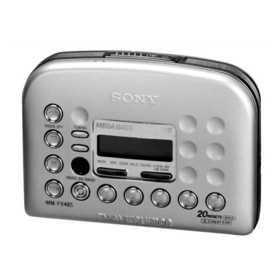
Photo : WM-FX485
Model Name Using Similar Mechanism
Tape Transport Mechanism Type
SPECIFICATIONS
Design and specifications are subject to change without notice.
RADIO CASSETTE PLAYER
US Model
WM-FX487
Canadian Model
WM-FX485/FX487
AEP Model
E Model
WM-FX483/FX485/FX487
WM-EX402/EX404/EX405/EX406
MF-WMFX483-147
Advertisement
Table of Contents

Related Manuals for Sony WM-FX483


Summary of Contents for Sony WM-FX483
- Page 1 WM-FX483/FX485/FX487 SERVICE MANUAL US Model WM-FX487 Ver 1.0 1998.03 Canadian Model WM-FX485/FX487 AEP Model E Model WM-FX483/FX485/FX487 Photo : WM-FX485 Manufactured under license from Dolby Model Name Using Similar Mechanism WM-EX402/EX404/EX405/EX406 Laboratories Licensing Corporation. Tape Transport Mechanism Type MF-WMFX483-147 “DOLBY” and the double-D symbol a are trademarks of Dolby Laboratories Licensing Corporation.
-
Page 2: Table Of Contents
TABLE OF CONTENTS Flexible Circuit Board Repairing GENERAL ······································································ 3 • Keep the temperature of the soldering iron aroud 270˚ C during repairing. DISASSEMBLY • Do not touch the soldering iron on the same conductor of the 2-1. Cabinet (Front) Assy ·························································· 5 circuit board (within 3 times). -
Page 3: General
SECTION 1 GENERAL — 3 —... - Page 4 — 4 —...
-
Page 5: Disassembly
SECTION 2 DISASSEMBLY • This set can be disassembled in the order shown below. 2-1. CABINET (REAR) ASSY 2-2. MAIN BOARD 2-3. MECHANISM DECK 2-4. CASSETTE LID SUB ASSY 2-5. DISPLAY BOARD Note : Follow the disassembly procedure in the numerical order given. 2-1. -
Page 6: Cabinet (Front) Assy
2-2. MAIN BOARD 1 Screw (1.7 × 2.5), tapping MAIN board 3 PC board, flexible Cabinet (front) assy HEAD flexible board 2-3. MECHANISM DECK Mechanism deck • Use caution when installing the cassette holder assy Install the cassette holder with the spring (lid up) as shown below in the drawing so that it fits into the holes on the cabinet front assy. -
Page 7: Cassette Lid Sub Assy
2-4. CASSETTE LID SUB ASSY 3 Spring (lid up) Cassette lid sub assy Cassette lid sub assy Cabinet (front) assy • Press on the left & right clips from the rear of the Cabinet (front) assy, and remove the boss. Cabinet (front) assy 2-5. -
Page 8: Mechanical Adjustment
SECTION 3 SECTION 4 MECHANICAL ADJUSTMENT ELECTRICAL ADJUSTMENT PRECAUTION PRECAUTION Clean the following parts with a denatured-alcahol-moistened Specified voltage : 3.0V sweb : Switch and control position Playback head Pinch roller MENU switch MENU → TAPE → SET Rubber belt Capstan : NORM MENU →... - Page 9 TUNER SECTION [AM] [FM] Setting : Setting : RADIO ON/BAND switch : ON/AM RADIO ON/BAND switch : ON/FM AM Tuning Voltage Adjustment FM Tuning Voltage Adjustment digital voltmeter digital voltmeter MAIN board MAIN board (VT) (VT) (GND) – (GND) – AM TUNING VOLTAGE ADJUSTMENT FM TUNING VOLTAGE ADJUSTMENT Adjust for a 10.0 ±...
- Page 10 [MAIN BOARD] — SIDE A — AM TUNING VOLTAGE ADJUSTMENT FM TRACKING ADJUSTMENT AM TRACKING ADJUSTMENT L4 (FERRITE BAR ANTENNA) AM TRACKING ADJUSTMENT FM TUNING VOLTAGE ADJUSTMENT AM IF ADJUSTMENT [MAIN BOARD] — SIDE B — (VT) (GND) (ANT) — 10 —...
-
Page 11: Diagrams
SECTION 5 DIAGRAMS Note on Printed Wiring Board: Note on Schematic Diagram: • Y : parts extracted from the conductor side. • All capacitors are in µF unless otherwise noted. pF: µµF • 50 WV or less are not indicated except for electrolytics : Through hole. - Page 12 IC301 LA4585M IC331 NJM2185V 25 24 23 22 21 20 13 12 10 9 PRE2 PRE1 REV (L) MIX IN (R) REV (R) WEIGHT HP IN (R) FWD (R) BIAS FWD (L) CIRCUIT L.B.GAIN Ach BLOCK RIPPLE Bch BLOCK (same Ach) M.B.ON/OFF MIX.1 BOOST...
-
Page 13: Block Diagram
WM-FX483/FX485/FX487 5-1. BLOCK DIAGRAM REF DC AUDIO POWER AMP Q311 IC301 FM/AM RF,IF B.P.F FM RF IN L OUT 12 DATA MIX OUT FX485/487 MODEL REMO FX483 LOCAL/DX MODEL R CH DOLBY NR 10.7MHz Q101 MODEL FM IF IN R OUT 11... -
Page 14: Printed Wiring Board -Main Section
WM-FX483/FX485/FX487 5-2. PRINTED WIRING BOARD — MAIN SECTION — • Refer to page 11 for Note on Printed Wiring Board. J301 • Semiconductor MAIN BOARD MAIN BOARD (SIDE A) (SIDE B) Location FX487 MODEL Ref. No. Location REMO DATA C-10... -
Page 15: Schematic Diagram -Main Section
WM-FX483/FX485/FX487 5-3. SCHEMATIC DIAGRAM — MAIN SECTION — • Refer to page 11 for Note on Schematic Diagram. — 17 — — 18 —... -
Page 16: Printed Wiring Board -Display Section-(Fx483/Fx485)
WM-FX483/FX485/FX487 5-4. PRINTED WIRING BOARD — DISPLAY SECTION — • Refer to page 11 for Note on Printed Wiring Board. (FX483/FX485) DISPLAY BOARD DISPLAY BOARD (SIDE A) (SIDE B) JC701 S705 S704 S702 S703 /RADIO OFF FX485 MODEL FX483 S706... - Page 17 WM-FX483/FX485/FX487 5-5. SCHEMATIC DIAGRAM — DISPLAY SECTION — • Refer to page 11 for Note on Schematic Diagram. (FX483/FX485) — 21 — — 22 —...
-
Page 18: Printed Wiring Board -Display Section-(Fx487)
WM-FX483/FX485/FX487 5-6. PRINTED WIRING BOARD — DISPLAY SECTION — • Refer to page 11 for Note on Printed Wiring Board. (FX487) DISPLAY BOARD DISPLAY BOARD (SIDE A) (SIDE B) • Semiconductor Location S707 Ref. No. Location MENU S711 IC701 G-11 AEP,IT,FR,C&SA,... -
Page 19: Schematic Diagram -Display Section-(Fx487)
WM-FX483/FX485/FX487 5-7. SCHEMATIC DIAGRAM — DISPLAY SECTION — • Refer to page 11 for Note on Schematic Diagram. (FX487) — 25 — — 26 —... -
Page 20: Ic Pin Function
5-8. IC PIN FUNCTION IC701 TC9327F Pin No. Pin Name Function 1–4 COM1–COM4 — Common terminal 5–22 S1–S18 — Segment terminal 23, 24 — Open MOTOR SPEED — Open SPEED - CTL — Open EL - CTL DOLBY Dolby control terminal (L: ON, Hi-imp: OFF) FWD/REV Head input selection terminal (L: REV, Hi-imp: FWD) —... - Page 21 Pin No. Pin Name Function XOUT — Crystal oscillator connection terminal — — Terminal to which external capacitor for stabilization of crystal oscillator power supply is connected VLCD — LCD drive power supply step-up terminal 78, 79 C1, C2 — —...
-
Page 22: Exploded Views
: Canadian KNOB, BALANCE (WHITE) . . . (RED) : Italian ↑ ↑ : East European Parts of Color Cabinet’s Color : French C & SA : Central and South America 6-1. CASSETTE LID SECTION WM-FX487 WM-FX483/FX485 — 29 —... - Page 23 Ref. No. Part No. Description Remarks Ref. No. Part No. Description Remarks 3-008-298-01 SCREW (FX487) 3-019-497-01 BUTTON (TOP) (FX487) 3-375-114-31 SCREW (FX483, FX485) 3-019-509-01 BUTTON (TOP) (FX483, FX485) 3-019-511-01 HOLDER (COVER), CASSETTE 3-026-812-01 BUTTON (MENU) (BLUE) (FX485: FR) (FX483/FX485: CND, E, C&SA) 3-020-517-01 BUTTON (SET MENU) (FX483, FX485) 3-019-498-01 HOLDER (COVER), CASSETTE (FX487) 3-020-517-21 BUTTON (SET MENU) (BLUE) (FX485: FR)
-
Page 24: Cabinet Section
6-2. CABINET SECTION MF-WMFX483-147 Ref. No. Part No. Description Remarks Ref. No. Part No. Description Remarks 3-020-510-01 KNOB (HOLD) (FX483) 3-020-507-01 CABINET (FRONT) (FX485: CND, C&SA) 3-318-203-51 SCREW (B1.7×12), TAPPING 3-020-507-41 CABINET (FRONT) (FX485: AEP, IT, FR, EE, E) 3-020-508-51 CABINET (REAR) (FX487) 3-020-507-51 CABINET (FRONT) (FX487) 3-020-508-31 CABINET (REAR) (FX483) 3-364-675-01 SPRING (CASSETTE) -
Page 25: Mechanism Deck Section
6-3. MECHANISM DECK SECTION (MF-WMFX483-147) HP901 M901 Ref. No. Part No. Description Remarks Ref. No. Part No. Description Remarks X-3375-020-1 LEVER ASSY (N-F), PINCH 3-703-816-31 SCREW (M1.4), SPECIAL HEAD X-3372-558-1 WHEEL ASSY (SP), CAPSTAN X-3375-021-1 LEVER ASSY (R-F), PINCH 3-354-868-11 BELT 3-703-816-73 SCREW (M1.4), SPECIAL HEAD 3-021-950-01 GEAR (DF) 3-921-797-01 WASHER... -
Page 26: Electrical Parts List
SECTION 7 DISPLAY ELECTRICAL PARTS LIST NOTE: • Due to standardization, replacements in the • RESISTORS When indicating parts by reference number, parts list may be different from the parts All resistors are in ohms. please include the board name. specified in the diagrams or the components METAL: metal-film resistor •... - Page 27 DISPLAY MAIN Ref. No. Part No. Description Remarks Ref. No. Part No. Description Remarks A-3021-077-A MAIN BOARD, COMPLETE (FX483: C&SA) R718 1-218-870-11 RES, CHIP 9.1K 0.50% 1/16W ********************* R719 1-218-836-11 RES, CHIP 0.50% 1/16W A-3021-078-A MAIN BOARD, COMPLETE R720 1-218-845-11 RES, CHIP 0.50% 1/16W ********************* R721...
- Page 28 MAIN Ref. No. Part No. Description Remarks Ref. No. Part No. Description Remarks 1-162-974-11 CERAMIC CHIP 0.01uF C402 1-164-357-11 CERAMIC CHIP 1000PF 1-124-434-00 ELECT 220uF C403 1-164-505-11 CERAMIC CHIP 2.2uF 1-115-156-11 CERAMIC CHIP C404 1-162-915-11 CERAMIC CHIP 10PF 0.5PF 1-115-156-11 CERAMIC CHIP C405 1-104-847-11 TANTAL.
- Page 29 MAIN Ref. No. Part No. Description Remarks Ref. No. Part No. Description Remarks < JACK > Q604 8-729-141-48 TRANSISTOR 2SB624-BV345 Q605 8-729-014-12 TRANSISTOR RN1311-TE85L J301 1-580-680-31 JACK (PHONES) Q606 8-729-028-76 TRANSISTOR DTA114YUA-T106 J302 1-750-061-11 JACK, DC (POLARITY UNIFIED TYPE) (DC IN) Q607 8-729-014-12 TRANSISTOR RN1311-TE85L Q608...
- Page 30 MAIN Ref. No. Part No. Description Remarks Ref. No. Part No. Description Remarks R106 1-216-820-11 METAL CHIP 1/16W R750 1-216-833-11 METAL CHIP 1/16W R107 1-216-807-11 METAL CHIP 1/16W (FR) < RESISTOR ARRAY > R107 1-216-795-11 RES, CHIP 1/16W (EXCEPT FR) RB701 1-233-810-21 RES, NETWORK 100K (3216) R108...
- Page 31 WM-FX483/FX485/FX487 Sony Corporation 98C1683-1 Printed in Japan © 1998.3 Personal A&V Products Company 9-923-373-11 Published by Quality Engineering Dept. — 38 — (Shibaura)
Need help?
Do you have a question about the WM-FX483 and is the answer not in the manual?
Questions and answers