Table of Contents
Advertisement
Quick Links
SS-US501/SW-US501/UZ-US501
SERVICE MANUAL
Ver 1.0 2004.01
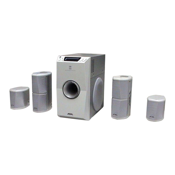
SS-US501
(SURROUND)
• UZ-US501 consists of the following models respectively.
Subwoofer
Front/Center Speakers
Surround Speakers
For the U.S.A. model
AUDIO POWER SPECIFICATIONS
POWER OUTPUT AND TOTAL
HARMONIC DISTORTION:
With 4 ohms loads subwoofer driven, from
20 - 200 Hz; rated 20 watts minimum RMS
power, with no more than 0.8% total
harmonic distortion from 250 milliwatts to
rated output.
SW-US501 (Subwoofer)
Max. output
Subwoofer:
30 W (4 ohms)
Front:
14 W + 14 W (8 ohms)
Dual center*:
14 W (4 ohms + 4 ohms)
Surround*:
14 W + 14 W (8 ohms)
* Depending on the sound field settings and the
source, there may be no sound output.
Speaker system Bass reflex type
Speaker unit
130 mm (5
1
/
in.) dia.
8
cone type
Dimensions (approx.)
160 × 300 × 300 mm
× 11
× 11
(6
3
/
7
/
8
8
(w/h/d, not including the
projecting parts)
Mass (approx.) 5.8 kg (12 lb 13 oz)
SS-US501 (Front/Center speakers)
Speaker system Front:
Closed box type
Center: Uni directional type
Sony Corporation
9-877-530-01
2004A05-1
Aiwa Original Products
C 2004.01
Published by Sony Engineering Corporation
SS-US501
SW-US501
(FRONT/CENTER)
(SUBWOOFER)
UZ-US501
SW-US501
SS-US501
SPECIFICATIONS
Speaker unit
Front:
Center: 48 mm (1
Rated impedance
Front:
Center: 4 ohms + 4 ohms
Dimensions (approx.)
85 × 200 × 125 mm
(3
3
(w/h/d, not including the
projecting parts)
Mass (approx.) 650g (1 lb 7 oz) × 2
Length of cable 3 m (9 ft.)
SS-US501 (Surround speakers)
Speaker system Closed box type
Speaker unit
58 mm (2
Rated impedance 8 ohms
Dimensions (approx.)
85 × 106 × 125 mm
(3
3
(w/h/d, not including the
projecting parts)
7
/
in.)
8
Mass (approx.) 350g (13 oz) × 2
Length of cable 8 m (24 ft.)
SS-US501
(FRONT/CENTER)
This system incorporates Dolby* Digital and Pro Logic Surround and
the DTS** Digital Surround System.
* Manufactured under license from Dolby Laboratories.
Dolby , Pro Logic , and the double-D symbol are trademarks of
Dolby Laboratories.
** Manufactured under license from Digital Theater Systems, Inc. DTS and
DTS Digital Surround are registered trademarks of Digital Theater Systems, Inc.
58 mm (2
3
/
in.) dia.
General
8
cone type
Power requirements
15
/
in.) dia.
16
U.S.A. model:
cone type
Other model:
8 ohms
Power consumption
U.S.A. model:
× 7
× 5 in.)
/
7
/
8
8
Other model:
Operating temperature
Operating humidity
Supplied accessories
3
/
in.) dia. cone type
8
× 4
× 5 in.)
/
1
/
8
4
Design and specifications are subject to change
without notice.
USB ACTIVE SPEAKER SYSTEM
US Model
AEP Model
UK Model
E Model
SS-US501
(SURROUND)
120 V AC, 60 Hz
220-240 V AC,
50/60 Hz
75 W
1.2 W
(at the Power Saving Mode)
75 W
0.3 W
(at the Power Saving Mode)
5ßC to 35ßC
5 % to 90 %
USB cable 1.8 m
(5.9 ft.) (1)
Remote commander
(remote) RM-Z7S101 (1)
CD-ROM WinDVD (1)
Operating Instructions
(this book) (1)
Advertisement
Table of Contents

Related Manuals for Sony SS-US501


Summary of Contents for Sony SS-US501
- Page 1 Mass (approx.) 5.8 kg (12 lb 13 oz) SS-US501 (Front/Center speakers) USB ACTIVE SPEAKER SYSTEM Speaker system Front: Closed box type Center: Uni directional type Sony Corporation 9-877-530-01 2004A05-1 Aiwa Original Products C 2004.01 Published by Sony Engineering Corporation...
- Page 2 LINE WITH MARK 0 ON THE SCHEMATIC DIAGRAMS AND IN THE PARTS LIST ARE CRITICAL TO SAFE OPERATION. REPLACE THESE COMPONENTS WITH SONY PARTS WHOSE PART NUMBERS APPEAR AS SHOWN IN THIS MANUAL OR IN SUPPLEMENTS PUB- LISHED BY SONY.
-
Page 3: Table Of Contents
SS-US501/SW-US501/UZ-US501 SECTION 1 SERVICING NOTE TABLE OF CONTENTS • MODEL IDENTIFICATION – Rear View – SERVICING NOTE ..........GENERAL ..............ANALOG IN DISASSEMBLY SPEAKER 3-1. Disassembly Flow ............6 FRONT 3-2. Top Chassis ..............6 CENTER OPTICAL IN 3-3. DIGITAL Board .............. 7 SURROUND 3-4. -
Page 4: General
SS-US501/SW-US501/UZ-US501 SECTION 2 This section is extracted from GENERAL instruction manual. Index to Parts and Controls Subwoofer (Front Panel) INPUT VOLUME PHONES AUTO POWER S-MODE 1 HEADPHONE jack (remote sensor) Connect headphones here. Receives the remote control signals. 2 AUTO POWER indicator... - Page 5 SS-US501/SW-US501/UZ-US501 Remote 1 MUTING, TEST TONE Mutes the sound. Pressing this button while pressing SHIFT will sound the test tone. MUTING 2 S-MODE, SET UP TEST TONE Selects the sound field mode. INPUT Pressing this button while pressing SHIFT will select the system menu.
-
Page 6: Disassembly
SS-US501/SW-US501/UZ-US501 SECTION 3 DISASSEMBLY • This set can be disassembled in the order shown below. 3-1. DISASSEMBLY FLOW 3-2. TOP CHASSIS (Page 6) 3-3. DIGITAL BOARD 3-4. FRONT CABINET SECTION (Page 7) (Page 7) Note: Follow the disassembly procedure in the numerical order given. -
Page 7: Digital Board
SS-US501/SW-US501/UZ-US501 3-3. DIGITAL BOARD 3 harness 2 screw (BVTP3 × 8) 5 connector (CN602) 4 connector (CN601) 7 two screws (BVTP3 × 10) 1 wire (flat type) (21 core) (CN801) 6 screw (BVTT3 × 8) 9 DIGITAL board 8 two screws (BVTP3 ×... -
Page 8: Test Mode
SS-US501/SW-US501/UZ-US501 SECTION 4 TEST MODE [TEST MODE] Procedure: 1. Press the button on the main set once while pressing the [S-MODE] button on the remote commander (RM-Z7S101) [INPUT] and the button on the main set. 2. When the test mode is activated, “USB” and “VOL” are displayed on the liquid crystal display. -
Page 9: Diagrams
SS-US501/SW-US501/UZ-US501 SECTION 5 DIAGRAMS 5-1. BLOCK DIAGRAM – MAIN Section – R-CH J701 HEADPHONE AMP IC605 PHONES MUTING MUTING Q613 Q700 MUTING MUTING HP MUTING CODEC, CONTROL SWITCH CONTROL SWITCH (Page 10) A/D, D/A CONVERTER, ELECTRICAL VOLUME Q821, 822 Q710, 711... -
Page 10: Block Diagram - Display/Power Supply Section
SS-US501/SW-US501/UZ-US501 5-2. BLOCK DIAGRAM – DISPLAY/POWER SUPPLY Section – STANDBY (Page 9) LIQUID CRYSTAL DISPLAY DRIVER AMP MUTING SYSTEM CONTROLLER (Page 9) IC701 IC802 (2/2) +10V FAN401 B+ SWITCH (EXCEPT US) REGULATOR (FAN) Q451, 452 Q453 MTR CTL (Page 9) -
Page 11: Note For Printed Wiring Boards And Schematic Diagrams
SS-US501/SW-US501/UZ-US501 5-3. NOTE FOR PRINTED WIRING BOARDS AND SCHEMATIC DIAGRAMS • Waveforms – DISPLAY Board – – DIGITAL Board – Note on Printed Wiring Boards: Note on Schematic Diagram: • X : parts extracted from the component side. • All capacitors are in µF unless otherwise noted. pF: µµF 1 IC501 t;... -
Page 12: Printed Wiring Board - Digital Board
SS-US501/SW-US501/UZ-US501 5-4. PRINTED WIRING BOARD – DIGITAL Board – :Uses unleaded solder. • Semiconductor Location DIGITAL BOARD (COMPONENT SIDE) Ref. No. Location D503 R569 R570 R571 R572 C529 R576 R575 D504 C530 R574 FB504 D802 F-15 R573 R605 C515 D803... -
Page 13: Schematic Diagram - Digital Board (1/5)
SS-US501/SW-US501/UZ-US501 5-5. SCHEMATIC DIAGRAM – DIGITAL Board (1/5) – • • See page 11 for Waveforms. See page 23 for IC Block Diagrams. • See page 26 for IC Pin Function Description. (1/5) FL507 FB508 +3.3V REGULATOR C561 C570 C507... -
Page 14: Schematic Diagram - Digital Board (2/5)
SS-US501/SW-US501/UZ-US501 5-6. SCHEMATIC DIAGRAM – DIGITAL Board (2/5) – • See page 11 for Waveform. • See page 26 for IC Pin Function Description. (2/5) HEAD PHONE BUS HP MUTE (Page 17) Q801 DTA114TKA-T R897 D806 R896 R895 R888 100k... -
Page 15: Schematic Diagram - Digital Board (3/5)
SS-US501/SW-US501/UZ-US501 5-7. SCHEMATIC DIAGRAM – DIGITAL Board (3/5) – • See page 23 for IC Block Diagram. (Page 13) (3/5) R542 C540 C512 R595 R539 4.7k 100k 4.7k C581 C552 C520 0.001 R553 R555 C519 330k C580 C884 220p C860... -
Page 16: Schematic Diagram - Digital Board (4/5)
SS-US501/SW-US501/UZ-US501 5-8. SCHEMATIC DIAGRAM – DIGITAL Board (4/5) – • See page 11 for Waveforms. • See page 26 for IC Pin Function Description. (Page 14) (4/5) LRCKO R833 (Page 13) C812 C899 C898 100p R841 C897 100p SDI2 LRCK... -
Page 17: Schematic Diagram - Digital Board (5/5)
SS-US501/SW-US501/UZ-US501 5-9. SCHEMATIC DIAGRAM – DIGITAL Board (5/5) – • See page 23 for IC Block Diagram. (5/5) C680 C644 0.47 R684 R631 2.2k HP.L A-GND C604 R630 6.8k C617 100p R605 R680 100k C607 C620 C621 0.47 R634 R635 0.47... -
Page 18: Printed Wiring Board - Display Board
SS-US501/SW-US501/UZ-US501 5-10. PRINTED WIRING BOARD – DISPLAY Board – :Uses unleaded solder. • Semiconductor Location Ref. No. Location D702 G-10 D703 D705 G-11 D706 G-11 D707 G-12 IC701 IC702 H-10 Q700 F-10 Q702 G-11 Q703 G-11 Q704 F-10 Q705 G-12... -
Page 19: Schematic Diagram - Display Board
SS-US501/SW-US501/UZ-US501 5-11. SCHEMATIC DIAGRAM – DISPLAY Board – • • See page 11 for Waveform. See page 23 for IC Block Diagram. (Page 14) -
Page 20: Printed Wiring Board - Amp Board
FRONT R918 (EXCEPT US) TO FRONT/CENTER C911 IC906 R903 C919 – – CENTER SPEAKER (L)/ (R), C901 JW408 SURROUND SPEAKER C927 Q905 (L)/(R) (SS-US501) JW409 – – C956 SURROUND R900 C950 CN451 R935 FB901 C952 C922 R934 JW401 L903 R901... -
Page 21: Schematic Diagram - Amp Board
SS-US501/SW-US501/UZ-US501 5-13. SCHEMATIC DIAGRAM – AMP Board – • See page 23 for IC Block Diagrams. CN401 (US) C409 C410 SP101 0.47 (WOOFER) (US) ∗ F901 ∗ C912 C920 L901 POWER AMP 3300p L903 5A 125V (US) JW901 330 200V (US) 10µH... -
Page 22: Printed Wiring Board
SS-US501/SW-US501/UZ-US501 5-15. SCHEMATIC DIAGRAM – SUB Board (Except US model) – 5-14. PRINTED WIRING BOARD – SUB Board (Except US model) – :Uses unleaded solder. AMP BOARD CN451 CN991 SUB BOARD (Page 20) LIVE R996 NEUTRAL C992 (Page 21) 0.01... - Page 23 SS-US501/SW-US501/UZ-US501 • IC Block Diagrams – DIGITAL Board – IC506 TPS78833DBVR IC805 AK4527BVQ 44 43 42 41 40 39 38 37 36 35 34 CURRENT LIMIT/ DZF2 THERMAL PROTECTION VREF RIN+ RIN– INPUT SDOS CIRCUIT LIN+ LIN– SMUTE ROUT1 BICK...
- Page 24 SS-US501/SW-US501/UZ-US501 IC801 LC89056W-E AUDIO C BIT PA/PB DETECT DETECT EMPHA SAMPLING XSEL FREQUENCY MICROCOMPUTER MODE0 INTERFACE MODE1 XOUT LOCK X’ TAL DGND DETECT XMCK DVDD 19 DVDD 18 DGND XSTATE DATAO LRCK DOSEL0 DATA TIMING DEMODULATOR DOSEL1 CKOUT CKSEL0 CKSEL1...
- Page 25 SS-US501/SW-US501/UZ-US501 – AMP Board – IC901 STR-F6424 (US Model) IC901 STR-F6676 (Except US Model) O.C.P/F.B O.C.P/F.B DRIVE DRIVE O.S.C O.S.C LATCH LATCH T.S.D T.S.D O.V.P O.V.P START REG. START REG. ICONST IC905 SI-8050JF OVER REGULATOR CURRENT PROTECTOR LATCH RESET &...
- Page 26 SS-US501/SW-US501/UZ-US501 • IC Pin Function Description DIGITAL BOARD IC501 TUSB3200ACPAH (USB CODEC) Pin No. Pin Name Description PLLFILO PLL loop filter output terminal AVDD — Power supply terminal (+3.3V) (analog system) PWMO PWM signal output terminal Not used PLLO PLL signal output terminal Not used DVSS —...
- Page 27 SS-US501/SW-US501/UZ-US501 DIGITAL BOARD IC502 DIT4096IPWR (DIGITAL AUDIO TRANSMITTER) Pin No. Pin Name Description Channel status data input terminal Not used COPY/C Copy protect signal or channel status serial data input terminal Not used Generation status signal input from the USB CODEC...
- Page 28 SS-US501/SW-US501/UZ-US501 DIGITAL BOARD IC802 µPD783033BYGF-M53-3BA-A (SYSTEM CONTROLLER) Pin No. Pin Name Description CO-DI Serial data output to the CODEC CO-CLK Serial data transfer clock signal output to the CODEC 3 to 5 — Not used DSP-DO Serial data input from the audio DSP...
- Page 29 SS-US501/SW-US501/UZ-US501 Pin No. Pin Name Description LCD-CS Chip select signal output to the LCD driver “L” active — Not used BVDD — Power supply terminal (+3.3V) (for bus interface) BVSS — Ground terminal (for bus interface) 60, 61 — Not used READY-H Power on/off control signal output terminal with APC “H”: power on...
- Page 30 SS-US501/SW-US501/UZ-US501 DIGITAL BOARD IC808 CXD9617R (AUDIO DIGITAL SIGNAL PROCESSOR) Pin No. Description Pin Name — Ground terminal XRST System reset signal input from the system controller “L”: reset EXTIN Master clock signal input terminal Not used Sampling frequency selection signal input terminal Not used —...
- Page 31 SS-US501/SW-US501/UZ-US501 Pin No. Description Pin Name WMD1 External memory wait mode setting terminal Fixed at “H” in this set — Ground terminal WMD0 External memory wait mode setting terminal Fixed at “H” in this set PAGE2 External memory page selection signal output terminal Not used —...
- Page 32 SS-US501/SW-US501/UZ-US501 Pin No. Description Pin Name SYNC Sync/non-sync setting terminal “L”: sync, “H”: non-sync Fixed at “H” in this set 117 to 119 — Ground terminal VDDI — Power supply terminal (+2.5V)
-
Page 33: Exploded Views
SS-US501/SW-US501/UZ-US501 SECTION 6 EXPLODED VIEWS NOTE: • -XX and -X mean standardized parts, so they • Items marked “*” are not stocked since they The components identified by mark 0 or dotted line with mark may have some difference from the original are seldom required for routine service. -
Page 34: Front Cabinet Section
SS-US501/SW-US501/UZ-US501 6-2. FRONT CABINET SECTION not supplied not supplied Ref. No. Part No. Description Remark Ref. No. Part No. Description Remark * 51 A-4750-582-A DISPLAY BOARD, COMPLETE A-4714-635-A FRONT CABINET ASSY (BLACK) 4-951-620-11 SCREW (2.6X10), +BVTP X-4956-145-1 LCD ASSY, WINDOW... -
Page 35: Main Section
SS-US501/SW-US501/UZ-US501 6-3. MAIN SECTION F901 not supplied not supplied not supplied The components identified by mark 0 or dotted line with mark 0 are critical for safety. Replace only with part number specified. Ref. No. Part No. Description Remark Ref. No. -
Page 36: Rear Chassis Section
SS-US501/SW-US501/UZ-US501 6-4. REAR CHASSIS SECTION EXCEPT US EXCEPT FAN401 The components identified by mark 0 or dotted line with mark 0 are critical for safety. Replace only with part number specified. Ref. No. Part No. Description Remark Ref. No. Part No. -
Page 37: Front/Surround Speaker Section
SS-US501/SW-US501/UZ-US501 6-5. FRONT/SURROUND SPEAKER SECTION Note: This set is the figure of Lch set. Ref. No. Part No. Description Remark Ref. No. Part No. Description Remark A-4713-395-A SPEAKER ASSY (L), SURROUND (WHITE) A-4713-841-A SPEAKER ASSY (R), FRONT (WHITE) A-4713-396-A SPEAKER ASSY (R), SURROUND (WHITE) -
Page 38: Electrical Parts List
SS-US501/SW-US501/UZ-US501 SECTION 7 ELECTRICAL PARTS LIST NOTE: • Due to standardization, replacements in the • Items marked “*” are not stocked since they The components identified by mark 0 or dotted line with mark parts list may be different from the parts speci- are seldom required for routine service. - Page 39 SS-US501/SW-US501/UZ-US501 Ref. No. Part No. Description Remark Ref. No. Part No. Description Remark C928 1-104-658-11 ELECT 100uF 0 IC901 8-749-017-79 IC STR-F6676 (EXCEPT US) 0 IC901 8-749-018-45 IC STR-F6424 (US) C929 1-104-662-11 ELECT 22uF IC902 6-700-388-01 IC SE-B2 (US) C931...
- Page 40 SS-US501/SW-US501/UZ-US501 DIGITAL Ref. No. Part No. Description Remark Ref. No. Part No. Description Remark R420 1-216-797-11 METAL CHIP 1/10W < TRANSFORMER > R421 1-216-845-11 METAL CHIP 100K 1/10W R425 1-216-845-11 METAL CHIP 100K 1/10W 0 T901 1-437-732-11 TRANSFORMER, POWER (US)
- Page 41 SS-US501/SW-US501/UZ-US501 DIGITAL Ref. No. Part No. Description Remark Ref. No. Part No. Description Remark C604 1-164-360-11 CERAMIC CHIP 0.1uF C822 1-164-360-11 CERAMIC CHIP 0.1uF C605 1-164-360-11 CERAMIC CHIP 0.1uF C823 1-164-360-11 CERAMIC CHIP 0.1uF C606 1-165-908-11 CERAMIC CHIP C607 1-104-666-11 ELECT...
- Page 42 SS-US501/SW-US501/UZ-US501 DIGITAL Ref. No. Part No. Description Remark Ref. No. Part No. Description Remark < CONNECTOR > < IC > CN601 1-506-990-11 PIN, CONNECTOR (PC BOARD) 8P * IC501 6-702-423-01 IC TUSB3200ACPAH CN602 1-573-913-11 PIN, CONNECTOR 15P IC502 6-705-391-01 IC DIT4096IPWR...
- Page 43 SS-US501/SW-US501/UZ-US501 DIGITAL Ref. No. Part No. Description Remark Ref. No. Part No. Description Remark Q821 8-729-055-92 TRANSISTOR SRA2203SF R553 1-216-833-11 METAL CHIP 1/10W Q822 8-729-024-91 TRANSISTOR 2SC2712-GL-TE85L R555 1-216-851-11 METAL CHIP 330K 1/10W < RESISTOR > R557 1-216-849-11 METAL CHIP...
- Page 44 SS-US501/SW-US501/UZ-US501 DIGITAL Ref. No. Part No. Description Remark Ref. No. Part No. Description Remark R647 1-216-833-11 METAL CHIP 1/10W R833 1-216-809-11 METAL CHIP 1/10W R648 1-216-845-11 METAL CHIP 100K 1/10W R834 1-216-809-11 METAL CHIP 1/10W R649 1-216-833-11 METAL CHIP 1/10W...
- Page 45 SS-US501/SW-US501/UZ-US501 DIGITAL DISPLAY Ref. No. Part No. Description Remark Ref. No. Part No. Description Remark R891 1-216-845-11 METAL CHIP 100K 1/10W L702 1-410-387-11 INDUCTOR 33uH R892 1-216-845-11 METAL CHIP 100K 1/10W R893 1-216-841-11 METAL CHIP 1/10W < LIQUID CRYSTAL DISPLAY >...
- Page 46 SS-US501/SW-US501/UZ-US501 Ref. No. Part No. Description Remark Ref. No. Part No. Description Remark < DIODE > D991 8-719-988-61 DIODE 1SS355TE-17 D992 8-719-053-18 DIODE 1SR154-400TE-25 D993 8-719-053-18 DIODE 1SR154-400TE-25 D994 8-719-053-18 DIODE 1SR154-400TE-25 D995 8-719-053-18 DIODE 1SR154-400TE-25 D996 8-719-988-61 DIODE 1SS355TE-17 <...
- Page 47 SS-US501/SW-US501/UZ-US501 MEMO...
-
Page 48: Revision History
SS-US501/SW-US501/UZ-US501 REVISION HISTORY Clicking the version allows you to jump to the revised page. Also, clicking the version at the upper right on the revised page allows you to jump to the next revised page. Ver. Date Description of Revision...
Need help?
Do you have a question about the SS-US501 and is the answer not in the manual?
Questions and answers