Advertisement
Quick Links
Download this manual
See also:
Service Manual
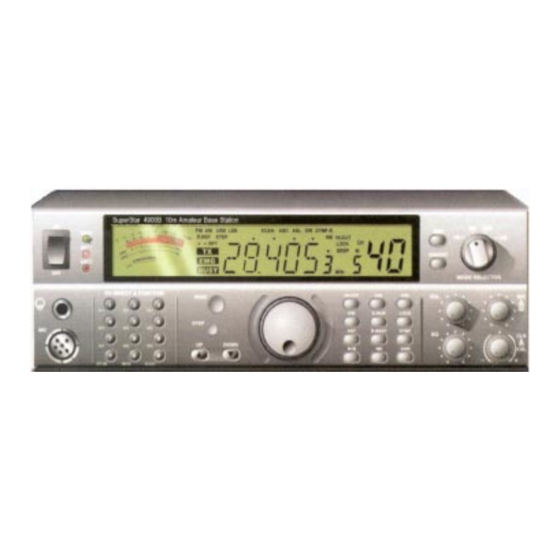
Super Star 4900B Service Manual
This is a on going project to document the Superstar 4900B. I have been working on this manual for several weeks. You
can display and print it but publication on the web and commercial use are not allowed.
If you have test equipment and a 4900B or can help in technical writing and/or research and would like to help on this
project go to the CBTricks Message Board and look for the Superstar documentation Discussion Group.
This manual is by no way complete.
Rev. History
Rev. # 1.0 Put up on the site
www.CBTricks.com
Advertisement

Subscribe to Our Youtube Channel
Related Manuals for Super Star 4900B


Summary of Contents for Super Star 4900B
- Page 1 If you have test equipment and a 4900B or can help in technical writing and/or research and would like to help on this project go to the CBTricks Message Board and look for the Superstar documentation Discussion Group.
- Page 2 SPECIFICATIONS GENERAL FREQUENCY COVERAGE 28.000 TO 29.690 MHz (10 METER BAND) 23.000 TO 29.600MHz (10 METER EXPENDED.) 26.965 TO 27.405MHz (CITIZEN BAND) 23.815 TO 30.555MHZ (600CHANEL CB BAND) FREQUENCY GENERATION BY MEANS OF PLL SYNTHESIZER FREQUENCY STABILITY ±0.001% OPERATING TEMPERATURE -10C TO +55C POWER SOURCE REQUIREMENTS AC 120V/5OHz or DC 16V...
- Page 3 Semiconductors And Function IC COMPLEMENT FUNCTION REF.NO TYPE MANUFACTURER MIC AMP IC-4 KIA4558F RESET IC-13 KIA7045F SQ COMPARATOR IC-2 NJM324 (M) DTMF DECODER IC-5 K55801S SAM SUNG DTMF ENCODER IC-6 KT3170 SAM SUNG BALANCE MODULATOR IC-12 TDA6130-5 IF DEMODULATOR IC-1 MC3361 MOTOROLA ASC COMPARATOR...
- Page 4 AUDIO PRE AMP KTC3875S AUDIO PRE AMP KTC3875S RF GAIN DRIVER KRC112S SWITCH FORANL KRC112S R/TX SWITCH KRC112S SWR SWITCH Q603 KRC112S NB AMP KTC3878 NB AMP KTC3878 TX IF AMP KTC3878 IF AMP KTC3878 IF AMP KTC3878 IF AMP KTC3878 IF AMP KTC3878...
- Page 5 xSS4900 Block Diagram...
- Page 6 SS4900 Adjustment Locations...
- Page 7 Test Equipment Required 1) CPU and Phase Locked Loop Section 1 Frequency Counter 2 DC Power Supply 3 DC Volt Meter 4 Oscilloscope 2) Transmitter Section 1 RF Power Meter (RF SSVM) 2 50Ω Load (non-inductive) 3 RF Attenuator 4 Oscilloscope 5 Audio Generator 6 DC Power Supply 7 Spectrum Analyzer...
- Page 8 2) Transmitter Section STEP SETTING CONNECTION ADJUST ADJUST FOR Connect oscilloscope probe to T216 Adjust for Maximum RF Driver Stage; Mode : Transmit base of Q72 T217 waveform on the Volume: Optional (Figure-3) T218 oscilloscope. Squelch : Optional T219 CH Selector:19 T220 ANT1 Without modulation...
- Page 9 Receiver Section STEP SETTING CONNECTION ADJUST ADJUST FOR Connect RF signal generator to (FM) Adjust the parts of RX Sensitivity; Mode: Receiver external ANT. Jack. Connect T201 tuning circuitry with Volume: Fully clockwise SSVM, Sinadder, T202 observing Squelch: Oscilloscope and distortion T203 ADM(Automatic Turn to counterclockwise...
- Page 10 Original Microphone Wiring Diagram: Pin # Description Mic Audio Receive Transmit Ch Down/Ch Up (2200 ohm resistors) Ground + 13.8 VDC (See Note Below) Warning: When wiring alternative microphones to this unit, Do Not short pin 6 to any other pins on the connector or damage to the unit may occur.
- Page 11 Semiconductor Lead Identification And Internal Diagrams IC’s ASC PCB IC-1 NJM324 M Main PCB IC-1 MC3361 (SMD)
- Page 12 Main PCB IC-2 KIA324F Main PCB IC-4...
- Page 13 Main PCB IC-5 Main PCB IC-6 KT3170 IN + Non inverting input of the op amp. IN - Inverting input of the op amp. Gain Select. VREF Reference Voltage output Input inhibit Control input for the stand-by power down mode. 7, 8 OSC1 OSC2 Clock input/output.
- Page 14 Main PCB IC-7 TMP87CM21DF CPU Pin Assignment PIN NAME REMARK DESCRIPTION ACTIVE GROUND XOUT 4.0MHz HIGH FREQUENCY CLOCK OUT 4.0MHz HIGH FREQUENCY CLOCK IN RESET RESET INPUT HIGH P22 (XOUT) OPEN DRAIN DIMMER OUT1 P21 (XTIN) OPEN DRAIN DIMMER OUT2 TEST FOXED TO LOW (GROUND) P20 (INT5/STOP)
- Page 15 P13 (DVO) TRI STATE TX OUT (OUT) ACTIVE “H” P14 (PPG) TRI STATE LC7152 DI (OUT) P15 (TC2) TRI STATE LC162 CLK (OUT) TRI STATE LC7152 ENABLE (OUT) TRI STATE LC7152 LDA (OUT) OPEN DRAIN EEPROM DATA OPEN DRAIN EEPROM CLOCK OPEN DRAIN FREQUENCY SHIFT 0.5KHz (OUT) ACTIVE “H”...
- Page 16 Main PCB IC-8 X24C02 DESCRIPTION A0 A1 A2 Address Inputs Serial Data Serial Clock Write Control Ground Supply Voltage...
- Page 17 Main PCB IC-9 LC7152M Symbol Function Symbol Function Side-B oscillator signal input Sub charge pump PDB2 Crystal oscillator Main charge pump PDB1 Low-pass filter transistors XOUT Side-A oscillator signal output Power supply General-purpose output port OUTB Ground Side-A unlock detection Serial data input Chip enable Sub charge pump...
- Page 18 Main PCB IC-10 78L05 (SOT-89) Main PCB IC-11 KIA7217AP...
- Page 19 Main PCB IC-12 TDA6130-5 Main PCB IC-13 KIA7045F Main PCB IC-14 KIA7810 (TO-220)
- Page 20 Front PCB IC-401 LC75854W...
- Page 21 Semiconductor Lead Identification And Internal Diagrams Transistors SMT Transistors (SOT23) KRC107 KRA102S KRC110S KRA104 KTC3878 KTA1504S KTC3879 KTC3880S Device Mark KRA102S KRA104 KTA1504S KRC107 KRC110S KTC3878 KTC3879 KTC3880S...
- Page 22 Transistors KTA1940 2SC 1969(CH) 2SC 2166...
- Page 23 Semiconductor Lead Identification And Internal Diagrams Diodes...
- Page 24 SS4900 Main PCB Component Layout...
- Page 25 SS4900 Main PCB Top Pattern...
- Page 26 SS4900 Main PCB Bottom Pattern...
- Page 27 SS4900 Front PCB Component Layout Top and Bottom...
- Page 28 SS4900 Front PCB Pattern Top and Bottom...
- Page 29 SS4900 Power Supply PCB Component Layout Top and Bottom...
- Page 30 SS4900 Power Supply PCB Pattern Top and Bottom Top Pattern Bottom Pattern...
- Page 31 SS4900 ASC PCB Component Layout Top and Bottom SS4900 ASC PCB Pattern Top and Bottom...
- Page 32 SS4900 DIN Jack PCB Component Layout Top and Bottom Pattern Top Pattern Bottom Pattern...
- Page 33 SS4900 Sub-D9 PCB Component Layout Top and Bottom Pattern Description Switched supply voltage 13.2 Vdc Ground AF out (needed for Voice Recorder, Tape 5 Tone Selective Call System) AF in PTT (low = TX) and FM-AF + Noise (Used for AKE FM – Select.) Squelch input (High = Signal is squelched, used for 5-Tone, AKE FM-Select.) Bottom Pattern...
- Page 34 SS4900 VR PCB’s Component Layout Top and Bottom Pattern...
- Page 35 SS4900 Channel Switch PCB Component Layout Top and Bottom Pattern...
-
Page 36: Specification
Still working on the following parts lists. CHANNEL PCB CODE NO. DESCRIPTION SPECIFICATION LOCATION 80213018 ASSY CH.PCB 15210106 RESISTOR-FIXED 10M-J-1/16W (0603) 15210153 RESISTOR-FIXED 15K-J-1/16W (0603) 15210390 RESISTOR-FIXED 39-J-1/16W (0603) 15210391 RESISTOR-FIXED 390-J-1/16W (0603) 32420036 CON-ASSY 45M/M, 3PIN (B/R/W) 35420006 SWITCH-PULSE YPS-210115SK SW402 M40E136B... - Page 37 RESISTOR-FIXED 10K-J-1/16W (0603) 15210103 R420 RESISTOR-FIXED 22K-J-1/16W (0603) 15210223 R421 RESISTOR-FIXED 470-J-1/16W (0603) 15210471 R423 RESISTOR-FIXED 2.7K-J-1/16W (0603) 15210272 R424 RESISTOR-FIXED 1K-J-1/16W (0603) 15210102 R425 RESISTOR-FIXED 100-J-1/16W (0603) 15210101 R427 RESISTOR-FIXED 4.7K-J-1/16W (0603) 15210472 R428 RESISTOR-FIXED 6.8K-J-1/16W (0603) 15210682 R431 RESISTOR-FIXED 6.8K-J-1/16W (0603) 15210682...
- Page 38 CONNECTOR PLUG S/T 6PIN 32420029 J404,J403 CONNECTOR PLUG S/T 3PIN 32420030 J405 CON-ASSY LOCK, 100M/M, 15PIN 32420041 CON-1 CON-ASSY 8283,250M/M, 6PIN 32420061 CON-2 DG-M910 28020019 LCD1 BACKLIGHT BS-27 28410003 LED LAMP DKL 30RD 28420001 D412,D411 209EGW/S209 28420003 D407 35020002 SWITCH-TACT DT1 101A 35020002 SWITCH-TACT...
- Page 39 MAIN TRANS CHASSIS EGI 1T 62000088 SCREW-PH, T/P2 (+) M3*L6, FNW 68000022 WASHER-PLAIN M4, FNW 68000025 SCREW-B/H M/C (+) M4*L12, FZY 68000060 WASHER-SPRING M4, FZY 68000061 LOCATION DESCRIPTION SPECIFICATION CODE NO. ASSY DC SUPPLY PCB 80229023 PCB-BS-27POWER 40*95,1 .6T,S/S M40E132D C-CERAMIC (DISK) 0.022UF-K-50V SL 17040022...
- Page 40 ASC PCB LOCATION DESCRIPTION SPECIFICATION CODE NO. ASSY MAIN PCB 80229014 ASSY ASC PCB 80213024 NJM324 (M) 11610018 TR-PNP KRA104 13010012 TR-NPN KRC110S 13210001 TR-NPN KRC112S 13210011 TR-PNP KTA1504S 13010004 TR-NPN KRC110S 13210001 RESISTOR-FIXED 27K-J-1/16W (0603) 15210273 RESISTOR-FIXED 6.8K-J-1/16W (0603) 15210682 RESISTOR-FIXED 12K-J-1/16W (0603)
- Page 41 MAIN PCB 8022902S ASSY MAIN B’D 80229028 ASSY MAIN SMD REF. DESCRIPTION SPECIFICATION CODE NO. MC3361 (SMD) 11610044 IC-1 KIA324F (SMD) 1161004S IC-2 UPC1037AH 11610050 IC-3 OP-AMP KIA4558F 11610003 IC-4 K558015 11610041 IC-5 KT3170 11610042 IC-6 TMP87CM21DF 11610046 IC-7 IC- EEPROM X24C02F 2KBIT SMD 11620002 IC-8...
- Page 42 TRANSISTOR KTC3205, TO-92L 13210048 TR-NPN KRC110S 13210001 TR-NPN KTC3875S 13210009 TR-NPN KTC3875S 13210009 TRANSISTOR KTA1940 13220014 TRANSISTOR KTA200, TO-92 13210047 TRANSISTOR KTC200, TO-92 13210046 TR-NPN KTC3875S 13210009 TRANSISTOR KTC3879 13210050 TR—NPN 2SC2314 13220003 TRANSISTOR 25C2166(C) 13220013 TR—NPN 25C1969 (CH) 13220004 TR—NPN 25C1969 (CH) 13220004...
- Page 43 REF. LOC. DESCRIPTION SPECIFICATION CODE NO. RESISTOR-FIXED 100K-J-1/16W (0603) 15210104 RESISTOR-FIXED 1K-J-1/16W (0603) 15210102 RESISTOR-FIXED 220K-J-1/16W (0603) 15210224 RESISTOR-FIXED 1K-J-1/16W (0603) 15210102 RESISTOR-FIXED 100-J-1/16W (0603) 15210101 RESISTOR-FIXED 100K-J-1/16W (0603) 15210104 RESISTOR-FIXED 10K-J-1/16W (0603) 15210103 RESISTOR-FIXED 470K-J-1/16W (0603) 15210474 RESISTOR-FIXED 6.8K-J-1/16W (0603) 15210682 RESISTOR-FIXED 6.8K-J-1/16W (0603)
- Page 44 RESISTOR-FIXED 470-J-1/16W (0603) 15210471 RESISTOR-FIXED 10K-J-1/16W (0603) 15210103 RESISTOR-FIXED 47K-J-1/16W (0603) 15210473 RESISTOR-FIXED 560-J-1/16W (0603) 15210561 RESISTOR-FIXED 1.5K-J-1/16W (0603) 15210152 RESISTOR-FIXED 220K-J-1/16W (0603) 15210224 RESISTOR-FIXED 680-J-1/16W 15210681 R101 RESISTOR-FIXED 10K-J-1/16W (0603) 15210103 R102 RESISTOR-FIXED 1.5K-J-1/16W (0603) 15210152 R103 RESISTOR-FIXED 22K-J-1/16W (0603) 15210223 R104 RESISTOR-FIXED...
- Page 45 RESISTOR-FIXED 10K-J-1/16W (0603) 15210103 R186 RESISTOR-FIXED 3.3K-J-1/16W (0603) 15210332 R187 RESISTOR-FIXED 4.7K-J-1/16W (0603) 15210472 R188 RESISTOR-FIXED 10K-J-1/16W (0603) 15210103 R189 RESISTOR-FIXED 2.2K-J-1/16W (0603) 15210222 R191 RESISTOR-FIXED 4.7K-J-1/16W (0603) 15210472 R192 RESISTOR-FIXED 100K-J-1/16W (0603) 15210104 R201 RESISTOR-FIXED 10K-J-1/16W (0603) 15210103 R205 RESISTOR-FIXED 10K-J-1/16W (0603) 15210103...
- Page 46 RESISTOR-FIXED 2.2K-J-1/16W (0603) 15210222 R287 RESISTOR-FIXED 10K-J-1/16W (0603) 15210103 R288 RESISTOR-FIXED 68-J-1/16W (0603) 15210680 R289 RESISTOR-FIXED 3.9-1W 160203R9 R290 RESISTOR-FIXED 5.6K-J-1/16W (0603) 15210562 R291 RESISTOR-FIXED 1.5K-J-1/16W (0603) 15210152 R292 RESISTOR-FIXED 470-J-1/16W (0603) 15210471 R293 RESISTOR-FIXED 18K-J-1/16W (0603) 15210183 R294 RESISTOR-FIXED 10K-J-1/16W (0603) 15210103 R295...
- Page 47 RESISTOR-FIXED 10K-J-1/16W (0603) 15210103 R606 RESISTOR-FIXED 10K-J-1/16W (0603) 15210103 R607 RESISTOR-FIXED 10K-J-1/16W (0603) 15210103 R608 RESISTOR-FIXED 100K-J-1/16W (0603) 15210104 R609 RESISTOR-FIXED 100K-J-1/16W (0603) 15210104 R611 RESISTOR-FIXED 100K-J-1/16W (0603) 15210104 R612 RESISTOR-FIXED 150K-J-1/16W (0603) 15210154 R613 RESISTOR-FIXED 150K-J-1/16W (0603) 15210154 R614 RESISTOR-FIXED 10K-J-1/16W (0603) 15210103...
- Page 48 C-CERAMIC GRM39 X7R 223K 25 17010223 C-CERAMIC GRM39 Y5V 473Z 50 17010473 C-CERAMIC GRM39 X7R 103K 50 17010103 C-CERAMIC GRM39 X7R 103K 50 17010103 C-CERAMIC GRM39 X7R 223K 25 17010223 C-CERAMIC GRM39 Y5V 473Z 50 17010473 C-CERAMIC GRM39 YSV 104Z 25 17010104 C-ELECT 47µF-M-16V, SMS...
- Page 49 C-CERAMIC GRM39 X7R 103K 50 17010103 C128 C-CERAMIC GRM39 COG 070D 50 17010070 C129 C-CERAMIC GRM39 X7R 103K 50 17010103 C131 C-ELECT 220µF-M-16V, SHL 18020227 C132 C-CERAMIC GRM39 X7R 103K 50 17010103 C133 C-CERAMIC GRM39 COG 101J 50 17010101 C135 C-ELECT 47µF-M-16V, SMS 18050047...
- Page 50 C-ELECT 0.22µF-M-50V, SMS 18050224 C225 C-CERAMIC GRM39 Y5V 473Z 50 17010473 C226 C-ELECT 220µF-M-16V, SHL 18020227 C227 C-ELECT 33µF-M-25V, SMS 18050033 C228 C-CERAMIC GRM39 X7R 472K 50S 17010472 C230 C-CERAMIC GRM39 Y5V 473Z 50 17010473 C231 C-ELECT 47µF-M-16V, SMS 18050047 C232 C-ELECT 1000µF-M-25V, SMS...
- Page 51 C-CERAMIC GRM39 COG 030C 50 17010030 C314 C-CERAMIC GRM39 X7R 103K 50 17010103 C315 C-CERAMIC GRM39 X7R 103K 50 17010103 C317 C-CERAMIC GRM39 COG 101J 50 17010101 C318 C-CERAMIC GRM39 X7R 103K 50 17010103 C319 C-CERAMIC GRM39 X7R 472K 50S 17010472 C320 C-CERAMIC (DISK)
- Page 52 REF. DESCRIPTION SPECIFICATION CODE NO. DIODE-GERMANUM 1N60 19820003 DIODE-GERMANUM 1N60 19820003 DIODE-SWITCH KDS184 19610003 DIODE-SWITCH KDS184 19610003 DIODE-GERMANUM 1N60 19820003 DIODE-SWITCH KDS184 19610003 DIODE-SWITCH KD5226 19610002 DIODE-VAR.CAPACITOR KDV2515 20210001 DIODE-VAR.CAPACITOR KDV2515 20210001 DIODE-SWITCH KDS184 19610003 DIODE-SWITCH KDS184 19610003 D19A DIODE-SWITCH KDS181 19610001 DIODE-SWITCH...
- Page 53 DIODE-SWITCH KDS184 19610003 D111 DIODE-SWITCH KDS184 19610003 D600 DIODE-SWITCH KDS184 19610003 D601 REF. DESCRIPTION SPECIFICATION CODE NO. COIL CHOKE 1 UH, CORE, 0.4 PI, 8 TURN 21220001 COIL-IFT 0031A 2142031A T201 COIL-IFT LB302 21420059 T202 COIL-IFT LB302 21420059 T203 COIL-IFT LB304 21420061 T204...
- Page 54 LOCATION DESCRIPTION SPECIFICATION CODE NO. X-TAL 10.241 Mhz, 49/U 23020028 X-TAL 3.579545 Mhz, 49/U 23020029 X-TAL 49/U, 4.5 Mhz 23020039 X-TAL 10.6975 Mhz, 49/U 23020031 X-TAL FILTER 10M 7.5B 10.695 Mhz 24220010 CF-1 X-TAL FILTER 10M 7.5B 10.695 Mhz 24220010 CF-2 FILTER-CERAMIC CFWS455HT...
- Page 55 15210103 RESISTOR-FIXED 10K-J-1/16W (0603) R805 15210103 RESISTOR-FIXED 10K-J-1/16W (0603) R806 15210103 RESISTOR-FIXED 10K-J-1/16W (0603) R807 15210103 RESISTOR-FIXED 10K-J-1/16W (0603) R809 15210273 RESISTOR-FIXED 27K-J-1/16W (0603) R810 15210682 RESISTOR-FIXED 6.8K-J-1/16W (0603) 17010103 C-CERAMIC GRM39 X7R 103K 50 C801 17010103 C-CERAMIC GRM39 X7R 103K 50 C802 17010102 C-CERAMIC...
- Page 56 32420049 CON—ASSY LOCK,350M/M,2PIN 62000085 MAIN TOP CHASSIS EGI iT 68000030 NUT—HEXAGON M3, FZY 4 68000053 SCREW—F/H M/C (+)M3*L6,FZB 70000105 SPEAKER FELT FELTO.5T 80229004 ASSY FRONT 61000489 VOLUME KNOB BLK SPRAY 61000571 VOLUME KNOB ABS 61000490 CHANNEL KNOB BLK SPRAY 61000572 CHANNEL KNOB ABS 61000491 DUAL INNER KNOB...
Need help?
Do you have a question about the 4900B and is the answer not in the manual?
Questions and answers