Advertisement
Quick Links
Super Star 4900B Service Manual
This is a on going project to document the Superstar 4900B. I started working on this manual Dec 2000. You can display
and print it but publication on the web and commercial use are not allowed.
If you have test equipment and a 4900B or can help in technical writing and/or research and would like to help on this
project go to the CBTricks Message Board and look for the Superstar documentation Discussion Group.
Rev. History
Rev. # 1.0
(a) Put up on the site
Rev. # 1.1
(a) Worked on the Alignment hook-up diagrams.
(b) Put the parts lists with the board layouts
(c) Made a change to alignment layout
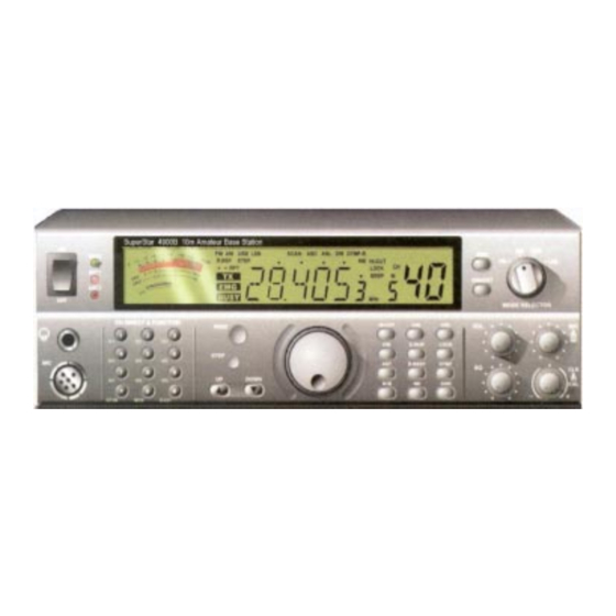
(d) Put a picture of the radio on first page.
(e) Schematic of the ASC PCB.
Rev. #1.2
(a) Schematic of MIC PCB
(b) Board Layouts MIC PCB
(c) AMC Mod Information
Next I need to work on the following sections.
Alignment Procedure
Export Frequency Modification
Parts List
Circuit descriptions
Semiconductor Information
Index page and index all the pages
www.CBTricks.com
This manual is by no way complete.
Advertisement

Subscribe to Our Youtube Channel
Related Manuals for Super Star 4900B

Summary of Contents for Super Star 4900B
- Page 1 If you have test equipment and a 4900B or can help in technical writing and/or research and would like to help on this project go to the CBTricks Message Board and look for the Superstar documentation Discussion Group.
- Page 2 SPECIFICATIONS GENERAL FREQUENCY COVERAGE 28.000 TO 29.690 MHz (10 METER BAND) 23.000 TO 29.600MHz (10 METER EXPENDED.) 26.965 TO 27.405MHz (CITIZEN BAND) 23.815 TO 30.555MHZ (600CHANEL CB BAND) FREQUENCY GENERATION BY MEANS OF PLL SYNTHESIZER FREQUENCY STABILITY ±0.001% OPERATING TEMPERATURE -10C TO +55C POWER SOURCE REQUIREMENTS AC 120V/5OHz or DC 16V...
- Page 3 Semiconductors And Function IC COMPLEMENT FUNCTION REF.NO TYPE MANUFACTURER MIC AMP IC-4 KIA4558F RESET IC-13 KIA7045F SQ COMPARATOR IC-2 NJM324 (M) DTMF DECODER IC-5 KS58015 SAM SUNG DTMF ENCODER IC-6 KT3170 SAM SUNG BALANCE MODULATOR IC-12 TDA6130-5 IF DEMODULATOR IC-1 MC3361 MOTOROLA ASC COMPARATOR...
- Page 4 AUDIO PRE AMP KTC3875S AUDIO PRE AMP KTC3875S RF GAIN DRIVER KRC112S SWITCH FORANL KRC112S RX / TX SWITCH KRC112S SWR SWITCH Q603 KRC112S NB AMP KTC3878 NB AMP KTC3878 TX IF AMP KTC3878 IF AMP KTC3878 IF AMP KTC3878 IF AMP KTC3878 IF AMP...
- Page 5 SS4900 Block Diagram...
- Page 6 SS4900 Adjustment Locations...
- Page 7 Test Equipment Required 1) CPU and Phase Locked Loop Section 1 Frequency Counter 2 DC Power Supply 3 DC Volt Meter 4 Oscilloscope 2) Transmitter Section 1 RF Power Meter (RF SSVM) 2 50Ω Load (non-inductive) 3 RF Attenuator 4 Oscilloscope 5 Audio Generator 6 DC Power Supply 7 Spectrum Analyzer...
- Page 8 2) Transmitter Section STEP SETTING CONNECTION ADJUST ADJUST FOR RF Driver Stage; Connect oscilloscope probe to T216 Adjust for Maximum Mode : Transmit base of Q72 T217 waveform on the Volume: Optional (Figure-3) T218 oscilloscope. Squelch : Optional T219 CH Selector:19 T220 ANT1 Without modulation...
- Page 9 Receiver Section STEP SETTING CONNECTION ADJUST ADJUST FOR RX Sensitivity; Connect RF signal generator to (FM) Adjust the parts of Mode: Receiver external ANT. Jack. Connect T201 tuning circuitry with Volume: Fully clockwise SSVM, Sinadder, T202 observing Squelch: Oscilloscope and distortion T203 ADM(Automatic Turn to counterclockwise...
- Page 10 Figure 2 Figure 1 Figure 3...
- Page 11 Figure 4 Figure 5 Figure 6...
- Page 12 Figure 7 Figure 8...
- Page 13 SS4900 AMC Limiter Modification To open the AMC (Automatic Modulation Control) circuit, locate Q43 (SMD) in grid location G1 on the main PCB. Carefully unsolder and lift the center pin up from the PCB, or remove the part entirely. Export Frequency Modification...
- Page 14 Microphone Wiring Information: Original Microphone Wiring Diagram: Pin # Description Mic Audio (White) Receive (Black) Transmit (Red) Ch Down/Ch Up (Blue) Ground (Shield) + 13.8 VDC (Green) (See Note Below) Warning: When wiring alternative microphones to this unit, Do Not short pin 6 to any other pins on the connector or damage to the unit may occur.
- Page 15 Semiconductor Lead Identification And Internal Diagrams IC’s ASC PCB IC-1 NJM324 M Main PCB IC-1 MC3361 (SMD)
- Page 16 Main PCB IC-2 KIA324F Main PCB IC-4...
- Page 17 Main PCB IC-5 Main PCB IC-6 KT3170 IN + Non inverting input of the op amp. IN - Inverting input of the op amp. Gain Select. VREF Reference Voltage output Input inhibit Control input for the stand-by power down mode. 7, 8 OSC1 OSC2 Clock input/output.
- Page 18 Main PCB IC-7 TMP87CM21DF CPU Pin Assignment PIN NAME REMARK DESCRIPTION ACTIVE GROUND XOUT 4.0MHz HIGH FREQUENCY CLOCK OUT 4.0MHz HIGH FREQUENCY CLOCK IN RESET RESET INPUT HIGH P22 (XOUT) OPEN DRAIN DIMMER OUT1 P21 (XTIN) OPEN DRAIN DIMMER OUT2 TEST FOXED TO LOW (GROUND) P20 (INT5/STOP)
- Page 19 P13 (DVO) TRI STATE TX OUT (OUT) ACTIVE “H” P14 (PPG) TRI STATE LC7152 DI (OUT) P15 (TC2) TRI STATE LC162 CLK (OUT) TRI STATE LC7152 ENABLE (OUT) TRI STATE LC7152 LDA (OUT) OPEN DRAIN EEPROM DATA OPEN DRAIN EEPROM CLOCK OPEN DRAIN FREQUENCY SHIFT 0.5KHz (OUT) ACTIVE “H”...
- Page 20 Main PCB IC-8 X24C02 DESCRIPTION A0 A1 A2 Address Inputs Serial Data Serial Clock Write Control Ground Supply Voltage...
- Page 21 Main PCB IC-9 LC7152M Symbol Function Symbol Function PDB2 Side-B oscillator signal input Sub charge pump Crystal oscillator PDB1 Main charge pump XOUT Low-pass filter transistors Side-A oscillator signal output OUTB Power supply General-purpose output port Ground Side-A unlock detection Serial data input Chip enable PDA2...
- Page 22 Main PCB IC-10 78L05 (SOT-89) Main PCB IC-11 KIA7217AP...
- Page 23 Main PCB IC-12 TDA6130-5 Main PCB IC-13 KIA7045F Main PCB IC-14 KIA7810 (TO-220)
- Page 24 Front PCB IC-401 LC75854W...
- Page 25 Semiconductor Lead Identification And Internal Diagrams Transistors SMT Transistors (SOT23) KRC107 KRA102S KRC110S KRA104 KTC3878 KTA1504S KTC3879 KTC3880S Device Mark KRA102S KRA104 KTA1504S KRC107 KRC110S KTC3878 KTC3879 KTC3880S...
- Page 26 Transistors KTA1940 2SC 1969(CH) 2SC 2166...
- Page 27 Semiconductor Lead Identification And Internal Diagrams Diodes...
- Page 28 SS4900 Main PCB Component Layout...
- Page 29 SS4900 Main PCB Top Pattern...
- Page 30 SS4900 Main PCB Bottom Pattern...
- Page 31 MAIN PCB 8022902S ASSY MAIN B’D 80229028 ASSY MAIN SMD REF. DESCRIPTION SPECIFICATION CODE NO. IC-1 MC3361 (SMD) 11610044 IC-2 KIA324F (SMD) 1161004S IC-3 UPC1037AH 11610050 IC-4 OP-AMP KIA4558F 11610003 IC-5 K558015 11610041 IC-6 KT3170 11610042 IC-7 TMP87CM21DF 11610046 IC-8 IC- EEPROM X24C02F 2KBIT SMD 11620002...
- Page 32 TR-NPN KRC110S 13210001 TR-NPN KTC3875S 13210009 TR-NPN KTC3875S 13210009 TRANSISTOR KTA1940 13220014 TRANSISTOR KTA200, TO-92 13210047 TRANSISTOR KTC200, TO-92 13210046 TR-NPN KTC3875S 13210009 TRANSISTOR KTC3879 13210050 TR—NPN 2SC2314 13220003 TRANSISTOR 25C2166(C) 13220013 TR—NPN 25C1969 (CH) 13220004 TR—NPN 25C1969 (CH) 13220004 TRANSISTOR KTC3879 13210050...
- Page 33 RESISTOR-FIXED 100K-J-1/16W (0603) 15210104 RESISTOR-FIXED 47K-J-1/16W (0603) 15210473 RESISTOR-FIXED 680-J-1/16W 15210681 RESISTOR-FIXED 22K-J-1/16W (0603) 15210223 RESISTOR-FIXED 1K-J-1/16W (0603) 15210102 RESISTOR-FIXED 47K-J-1/16W (0603) 15210473 RESISTOR-FIXED 3.3K-J-1/16W (0603) 15210332 RESISTOR-FIXED 10K-J-1/16W (0603) 15210103 RESISTOR-FIXED 10K-J-1/16W (0603) 15210103 RESISTOR-FIXED 1K-J-1/16W (0603) 15210102 RESISTOR-FIXED 10K-J-1/16W (0603) 15210103 RESISTOR-FIXED...
- Page 34 R152 RESISTOR-FIXED 220K-J-1/16W (0603) 15210224 R153 RESISTOR-FIXED 1.5K-J-1/16W (0603) 15210152 R154 RESISTOR-FIXED 100-J-1/16W (0603) 15210101 R155 RESISTOR-FIXED 1K-J-1/16W (0603) 15210102 R156 RESISTOR-FIXED 220K-J-1/16W (0603) 15210224 R157 RESISTOR-FIXED 1.5K-J-1/16W (0603) 15210152 R158 RESISTOR-FIXED 56-J-1/16W (0603) 15210560 R159 RESISTOR-FIXED 1K-J-1/16W (0603) 15210102 R161 RESISTOR-FIXED 100-J-1/16W (0603)
- Page 35 R249 RESISTOR-FIXED 100K-J-1/16W (0603) 15210104 R250 RESISTOR-FIXED 100K-J-1/16W (0603) 15210104 R255 RESISTOR-FIXED 10K-J-1/16W (0603) 15210103 R256 RESISTOR-FIXED 10K-J-1/16W (0603) 15210103 R258 RESISTOR-FIXED 10K-J-1/16W (0603) 15210103 R259 RESISTOR-FIXED 2.2K-J-1/16W (0603) 15210222 R261 RESISTOR-FIXED 2.2K-J-1/16W (0603) 15210222 R263 RESISTOR-FIXED 1M-J-1/16W (0603) 15210105 R264 RESISTOR-FIXED 1K-J-1/16W (0603)
- Page 36 R329 RESISTOR-FIXED 27-J-1/16W (0603) 15210270 R330 RESISTOR-FIXED 12K-J-1/16W (0603) 15210123 R333 RESISTOR-FIXED 22K-J-1/16W (0603) 15210223 R335 RESISTOR-FIXED 10K-J-1/16W (0603) 15210103 R339 RESISTOR-FIXED 100-J-1/16W (0603) 15210101 R341 RESISTOR-FIXED 1.5K-J-1/16W (0603) 15210152 R342 RESISTOR-FIXED 330-J-1/16W (0603) 15210331 R343 RESISTOR-FIXED 47-J-1/16W (0603) 15210470 R344 RESISTOR-FIXED 100-J-1/16W (0603)
- Page 37 REF. DESCRIPTION SPECIFICATION CODE NO. C-ELECT 22µF-M-16V, SMS 18050022 C-CERAMIC GRM39 COG 221 J50 17010221 C-CERAMIC GRM39 X7R 223K 25 17010223 C-CERAMIC GRM39 X7R 102K 50 17010102 C-CERAMIC GRM39 X7R 472K 50S 17010472 C-CERAMIC GRM39 X7R 103K 50 17010103 C-CERAMIC GRM39 X7R 102K 50 17010102 C-CERAMIC...
- Page 38 C-CERAMIC GRM39 X7R 472K 50S 17010472 C-ELECT 22µF-M-16V, SMS 18050022 C-CERAMIC GRM39 Y5V 473Z 50 17010473 C-CERAMIC GRM39 X7R 472K 50S 17010472 C-CERAMIC GRM39 COG 100D 50 17010100 C-CERAMIC GRM39 COG 101J 50 17010101 C-ELECT 0.47µF-SMS 5*11 18020R47 C-CERAMIC GRM39 COG 050C 50 17010050 C-CERAMIC GRM39 COG 100D 50...
- Page 39 C184 C-CERAMIC GRM39 Y5V 473Z 50 17010473 C186 C-ELECT 0.47µF-BP 18020474 C187 C-CERAMIC GRM39 X7R 102K 50 17010102 C188 C-CERAMIC GRM39 X7R 103K 50 17010103 C189 C-ELECT 47µF-M-16V, SMS 18050047 C191 C-CERAMIC GRM39 Y5V 473Z 50 17010473 C192 C-ELECT 22µF-M-16V, SMS 18050022 C193 C-CERAMIC...
- Page 40 C272 C-CERAMIC GRM39 COG 050C 50 17010050 C273 C-CERAMIC GRM39 COG 470J 50 17010470 C281 C-CERAMIC GRM39 X7R 103K 50 17010103 C281A C-CERAMIC GRM39 COG 330J 50 17010330 C282 C-CERAMIC GRM39 COG 221 J50 17010221 C283 C-CERAMIC GRM39 X7R 103K 50 17010103 C284 C-CERAMIC...
- Page 41 REF. DESCRIPTION SPECIFICATION CODE NO. DIODE-GERMANUM 1N60 19820003 DIODE-GERMANUM 1N60 19820003 DIODE-SWITCH KDS184 19610003 DIODE-SWITCH KDS184 19610003 DIODE-GERMANUM 1N60 19820003 DIODE-SWITCH KDS184 19610003 DIODE-SWITCH KD5226 19610002 DIODE-VAR.CAPACITOR KDV2515 20210001 DIODE-VAR.CAPACITOR KDV2515 20210001 DIODE-SWITCH KDS184 19610003 D19A DIODE-SWITCH KDS184 19610003 DIODE-SWITCH KDS181 19610001 D22A...
- Page 42 D111 DIODE-SWITCH KDS184 19610003 D600 DIODE-SWITCH KDS184 19610003 D601 DIODE-SWITCH KDS184 19610003 REF. DESCRIPTION SPECIFICATION CODE NO. COIL CHOKE 1 UH, CORE, 0.4 PI, 8 TURN 21220001 T201 COIL-IFT 0031A 2142031A T202 COIL-IFT LB302 21420059 T203 COIL-IFT LB302 21420059 T204 COIL-IFT LB304 21420061...
-
Page 43: Location Description
LOCATION DESCRIPTION SPECIFICATION CODE NO. X-TAL 10.241 Mhz, 49/U 23020028 X-TAL 3.579545 Mhz, 49/U 23020029 X-TAL 49/U, 4.5 Mhz 23020039 X-TAL 10.6975 Mhz, 49/U 23020031 CF-1 X-TAL FILTER 10M 7.5B 10.695 Mhz 24220010 CF-2 X-TAL FILTER 10M 7.5B 10.695 Mhz 24220010 CF-3 FILTER-CERAMIC... - Page 44 SS4900 Front PCB Component Layout Top and Bottom...
- Page 45 SS4900 Front PCB Pattern Top and Bottom...
- Page 46 FRONT PCB REF. DESCRIPTION SPECIFICATION CODE NO. ASSY FRONT PCB 80229011 ASSY FRONT SMD 80229019 PCB-BS-29-FRONT 81*266,1 .6T,D/S M40E151A ASSY FRONT INSERT 80229020 C401 C-CERAMIC GRM39 Y5V 104Z 25 17010104 C402 C-CERAMIC GRM39 X7R 681K J50 17010681 C403 C-CERAMIC GRM39 Y5V 473Z 50 17010473 C404 C-ELECT...
- Page 47 Q404 TR-PNP KRA102S 13010005 Q405 TR-NPN KRC112S 13210011 Q406 TR-NPN KRC112S 13210011 D401 DIODE-SWITCH KDS184 19610003 SW10 SWITCH-TACT SMD-1101 35010003 SW11 SWITCH-TACT SMD-1101 35010003 SW13 SWITCH-TACT SMD-1101 35010003 SW14 SWITCH-TACT SMD-1101 35010003 SW15 SWITCH-TACT SMD-1101 35010003 SW16 SWITCH-TACT SMD-1101 35010003 SW17 SWITCH-TACT SMD-1101...
- Page 48 SS4900 Power Supply PCB Component Layout Top and Bottom...
- Page 49 SS4900 Power Supply PCB Pattern Top and Bottom Top Pattern Bottom Pattern REF. DESCRIPTION SPECIFICATION CODE NO. ASSY DC SUPPLY PCB 80229023 PCB-BS-27POWER 40*95,1 .6T,S/S M40E132D C253 C-CERAMIC (DISK) 0.022UF-K-50V SL 17040022 C254 C-ELECT 10000UF/25V 18050109 C951 C-CERAMIC (DISK) 0.1UF-Z-50V 17040104 C952 C-CERAMIC (DISK)
- Page 50 SS4900 ASC PCB Component Layout Top and Bottom SS4900 ASC PCB Pattern Top and Bottom...
- Page 51 ASC PCB Schematic Diagram...
- Page 52 ASC PCB REF. DESCRIPTION SPECIFICATION CODE NO. ASSY MAIN PCB 80229014 ASSY ASC PCB 80213024 NJM324 (M) 11610018 TR-PNP KRA104 13010012 TR-NPN KRC110S 13210001 TR-NPN KRC112S 13210011 TR-PNP KTA1504S 13010004 TR-NPN KRC110S 13210001 RESISTOR-FIXED 27K-J-1/16W (0603) 15210273 RESISTOR-FIXED 6.8K-J-1/16W (0603) 15210682 RESISTOR-FIXED 12K-J-1/16W (0603)
- Page 53 SS4900 DIN Jack PCB Component Layout Top and Bottom Pattern Top Pattern Bottom Pattern 6 PIN DIN CON PCB REF. DESCRIPTION SPECIFICATION CODE NO ASSY 6 DIN JACK 80213027 PCB-BS-27-DIN JACK 45*25,0.8T,D/S M40E133C CON12 CON-ASSY 350M/M, 6PIN (6 COLOR) 32420048 C345 C-CERAMIC GRM39 X7R 472K 50S...
- Page 54 SS4900 Sub-D9 PCB Component Layout Top and Bottom Pattern Description Switched supply voltage 13.2 Vdc Ground AF out (needed for Voice Recorder, Tape 5 Tone Selective Call System) AF in PTT (low = TX) and FM-AF + Noise (Used for AKE FM – Select.) Squelch input (High = Signal is squelched, used for 5-Tone, AKE FM-Select.) Top Pattern...
- Page 55 9 PIN D-SUB PCB REF. DESCRIPTION SPECIFICATION CODE NO PCB-BS-27RS232 19*32,1 .6T,D/S M40E134B C372 C-CERAMIC GRM39 X7R 472K 50S 17010472 C373 C-CERAMIC GRM39 X7R 472K 50S 17010472 C374 C-CERAMIC GRM39 X7R 472K 50S 17010472 C375 C-CERAMIC GRM39 X7R 472K 50S 17010472 C376 C-CERAMIC...
- Page 56 SS4900 VR PCB’s Component Layout Top and Bottom Pattern VR PCB’s CODE NO. DESCRIPTION SPECIFICATION REF. 80229017 ASSY VOL PCB 1662A153 RESISTOR-VARIABLE V9MDN-3B10K+15A 50K 1662C203 RESISTOR-VARIABLE V9MDN-3B5K+3B 20K MIC VR403 1662C502 RESISTOR-VARIABLE V9MDN-3B20K+3B 5K CAL VR404 32420060 CON-ASSY 8283 (H+B) 70M/M, V 6PIN M40E137B PCB-BS-27-MIC VOL 9*26,0.8T,D/S...
- Page 57 SS4900 Channel Switch PCB Component Layout Top and Bottom Pattern CHANNEL PCB CODE NO. DESCRIPTION SPECIFICATION REF. 80213018 ASSY CH.PCB 15210106 RESISTOR-FIXED 10M-J-1/16W (0603) 15210153 RESISTOR-FIXED 15K-J-1/16W (0603) 15210390 RESISTOR-FIXED 39-J-1/16W (0603) 15210391 RESISTOR-FIXED 390-J-1/16W (0603) 32420036 CON-ASSY 45M/M, 3PIN (B/R/W) 35420006 SWITCH-PULSE YPS-210115SK...
- Page 58 SS4900 MIC PCB Component Layout Top and Bottom REF. DESCRIPTION SPECIFICATION CODE NO. PCB-EM-27-UP/DOWN 28.3*14.2*1 .2T M40E040A ASSY M/M BD SWITCH-TACT DT1 101A 35020002 SWITCH-TACT DT1 101A 35020002 SWITCH-TACT S/W TACT S/W, DT1101S 35010001 SWITCH-TACT S/W TACT S/W, DT1101S 35010001 SWITCH-TACT S/W TACT S/W, DT1101S 35010001...
- Page 60 REF. DESCRIPTION SPECIFICATION CODE NO. ASSY TRANS CHA 80229013 TF-2 TRANS BS-29 (E) 120V / 16V, 5A 26020009 MAIN TRANS CHASSIS EGI 1T 62000088 SCREW-PH, T/P2 (+) M3*L6, FNW 68000022 WASHER-PLAIN M4, FNW 68000025 SCREW-B/H M/C (+) M4*L12, FZY 68000060 WASHER-SPRING M4, FZY 68000061...
- Page 61 CODE NO. DESCRIPTION SPECIFICATION LOCATION 35420004 RELAY RY-12WK 26020008 TRANSFORMER-CHOKE 1 9MM,0.9P1 TF-1 32420020 CONNECTOR 4PIN 3M/M 32420028 PLUG STRAIGHT 00-8283-15 12 00000 32420029 CONNECTOR PULG S/T 6PIN 1 D—SUB 9PIN 32420030 CONNECTOR PULG S/T 3PIN 1 PHONE JACK 32420042 CONNECTOR PULG S/T 2PIN 3 32420042...
- Page 62 69000317 PAD “3—FRONT DW—2(210*i04) 2 69000329 BOX—GIFT SW—3(i.5—2T) 70000103 WINDOW TAPE(U) DOUBLE AD/TAPE 70000104 WINDOW TAPE(D) DOUBLE AD/TAPE 70000107 POLY BAG LDPEO.05T M4OEi SQA PCB—BS—29MA1N 169.1*198.2,1 .6T,D/S 80229007 ASSY BOTTOM 61000495 FRAME HINGE(R) PC, BLAK CODE NO. DESCRIPTION SPECIFICATION Q’TY LOCATION 61000496 FRAME HINGE(L)
- Page 63 61000576 COVER—FRONT 70000110 FELT—LCD FELT 0.5T,BLK 80229005 ASSY MAIN 62000087 MAIN FRONT CHASSIS EGI iT 62000089 MAIN RIGHT CHASSIS EGI iT 68000022 SCREW—P.H, T/P2 (+)M3*L6,FNW 80229012 ASSY BACK CHA 32020003 CONNECTOR—ANT(M) SO—239D J—3,J—4 32420052 JOINT—CONNECTOR YELLO—CAP JOINT 33010006 JACK TG—25N 2.5P1 WITHNUT J—i 35020009 SWITCH LOCKER...
Need help?
Do you have a question about the 4900B and is the answer not in the manual?
Questions and answers