Table of Contents
Advertisement
Quick Links
XR-MP50
EZ
SERVICE MANUAL
COMPACT DISC
BASIC TAPE MECHANISM : 2ZM-1 R11NM
STEREO SYSTEM
BASIC CD MECHANISM : 3ZG-3 E13NM
REMOTE
SPEAKER
SYSTEM
CONTROLLER
SX–M510
RC–AAT17
XR–MP50
• This Service Manual is the "Revision Publishing" and replaces "Simple Manual"
XR-MP50 (EZ), (S/M Code No. 09-00B-439-6T1).
S/M Code No. 09-011-439-6R1
Advertisement
Table of Contents

Related Manuals for Aiwa XR-MP50


Summary of Contents for Aiwa XR-MP50
- Page 1 BASIC TAPE MECHANISM : 2ZM-1 R11NM STEREO SYSTEM BASIC CD MECHANISM : 3ZG-3 E13NM REMOTE SPEAKER SYSTEM CONTROLLER SX–M510 RC–AAT17 XR–MP50 • This Service Manual is the “Revision Publishing” and replaces “Simple Manual” XR-MP50 (EZ), (S/M Code No. 09-00B-439-6T1). S/M Code No. 09-011-439-6R1...
-
Page 2: Table Of Contents
TABLE OF CONTENTS SPECIFICATIONS ................................3 PROTECTION OF EYES FROM LASER BEAM DURING SERVICING ............... 4 PRECAUTION TO REPLACE OPTICAL BLOCK ......................4 DISASSEMBLY INSTRUCTIONS ..........................5 ~ 8 NOTES DURING RE-ASSEMBLING ..........................9 ELECTRICAL MAIN PARTS LIST ........................... 10 ~ 15 TRANSISTOR ILLUSTRATION ............................ -
Page 3: Specifications
SPECIFICATIONS Main unit <General> <FM tuner section> Power requirements 230 V AC, 50 Hz Tuning range 87.5 MHz to 108 MHz Power consumption 90 W Usable sensitivity (IHF) 16.8 dBf Standby power consumption 1.0 W (power-economizing Antenna terminals 75 ohms (unbalanced) mode set to ON or AUTO) Dimensions of main unit 175 x 257 x 333 mm... -
Page 4: Protection Of Eyes From Laser Beam During Servicing
PROTECTION OF EYES FROM LASER BEAM DURING SERVICING CAUTION This set employs laser. Therefore, be sure to follow carefully the instructions below when servicing. Use of controls or adjustments or performance of procedures other than those specified herin may result in hazardous radiation expo- WARNING!! sure. -
Page 5: Disassembly Instructions
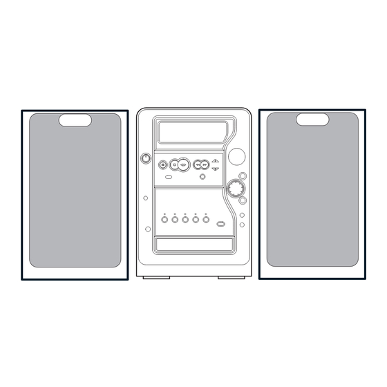
DISASSEMBLY INSTRUCTIONS 1. Removing the outside appearance parts 1) Remove the six screws (1-4, 2-2) and remove the PANEL, SIDE R. 2) Remove the six screws (1-4, 2-2) and remove the PANEL, SIDE L. 3) Remove the three screws 1 and lift up the PANEL, TOP ASSY 2. 4) Remove the two connectors and remove the PANEL, TOP ASSY. - Page 6 5) Remove the 11 screws and remove the CABI, REAR. 6) Remove the screw and JOINT, CABI. 7) This is the state after the outside appearance parts are removed. 2. Removing the PWB, CD AFP-4 1) Remove the five screws, pull out the FFC and other parts, then remove the PWB, CD AFP-4.
- Page 7 3. Removing the PWB, MAIN ASSY 1) Remove the screw 1, then remove the connector 2. 2) Remove the screw 1 and remove the PWB, MAIN ASSY 2 in the direction of the arrow. (The board is hooked. While lifting up the HOOK, remove the board.) 4.
- Page 8 2) Remove the two screws 1 and remove the CABI, FR ASSY in the direction of arrow 2. 5. Removing the CD board (3ZG-3) 1) Remove the four screws 1 and remove the CD block 2. 2) This is the state after the CD block is removed. –...
-
Page 9: Notes During Re-Assembling
NOTES DURING RE-ASSEMBLING When assemble the magical change panel, adjust the phase of the gear. 1. Phase adjustment of the GEAR, OPE 1 and GEAR, WORM WHEEL. 1) Align holes 1. 2) Then, move the position of the holes of each gear as shown by 2 in the illustration. HLDR, GEAR GEAR, WORM WHEEL GEAR, OPE 1... -
Page 10: Electrical Main Parts List
ELECTRICAL MAIN PARTS LIST REF. NO. PART NO. KANRI DESCRIPTION REF. NO. PART NO. KANRI DESCRIPTION 87-A40-270-080 C-DIODE,MC2838 87-A40-269-080 C-DIODE,MC2836 87-070-274-080 DIODE,1N4003 SEM 8A-FP4-608-030 C-IC,UPD784216AYGC-107-8EU 87-070-022-010 DIODE,IN5402 8A-AV6-605-030 C-IC,UT611024LC-12 87-A40-345-080 ZENER,MTZJ10C 87-A20-965-040 C-IC,S-80842ANNP-ED6 87-A21-021-040 C-IC,BU2099FV 87-A40-650-080 ZENER,MTZJ6.8A 87-A21-323-010 C-IC,CXD2585Q 87-A40-004-080 ZENER,MTZJ16A 87-070-322-080 ZENER,MTZJ 36D... - Page 11 REF. NO. PART NO. KANRI DESCRIPTION REF. NO. PART NO. KANRI DESCRIPTION C213 87-010-195-080 C-CAP,S 0.068-25 F C386 87-010-196-080 CHIP CAPACITOR,0.1-25 C214 87-010-195-080 C-CAP,S 0.068-25 F C388 87-012-156-080 C-CAP,S 220P-50 CH C215 87-012-368-080 C-CAP,S 0.1-50 F C389 87-010-380-080 CAP, ELECT 47-16V C216 87-012-368-080 C-CAP,S 0.1-50 F...
- Page 12 KANRI REF. NO. PART NO. KANRI DESCRIPTION REF. NO. PART NO. DESCRIPTION FC502 8A-CJ4-648-210 FF-CABLE,14P 1.0 CNA401 88-802-092-420 CONN ASSY,9P RED FC504 88-906-201-110 FF-CABLE,6P 1.25 D151 87-A40-317-080 LED,SLR-342VCT31 RED H101 87-A90-511-010 HLDR,WIRE 2.5-10P D152 87-A40-317-080 LED,SLR-342VCT31 RED J201 87-A60-420-010 JACK,3.5 ST (MSC) D153 87-A40-317-080 LED,SLR-342VCT31 RED...
- Page 13 KANRI REF. NO. PART NO. KANRI DESCRIPTION REF. NO. PART NO. DESCRIPTION C251 87-010-831-080 C-CAP,U,0.1-16F C759 87-016-459-080 CAP,E 470-10 SMG C252 87-010-831-080 C-CAP,U 0.1-16F C760 87-012-286-080 CAP, U 0.01-25 C253 87-010-382-080 CAP, ELECT 22-25V C762 87-010-831-080 C-CAP,U,0.1-16F C254 87-012-286-080 C-CAP,U,0.01-25 K B C771 87-012-274-080 CHIP CAP,U 1000P-50B...
- Page 14 KANRI REF. NO. PART NO. KANRI DESCRIPTION REF. NO. PART NO. DESCRIPTION SOL2 82-ZM3-628-010 SOL ASSY,23 SO R892 87-022-198-080 C-RES,S680 1/10WF 87-036-110-010 SW,MICRO SPPB62 R893 87-022-360-080 C-RES,S 39K-1/10WF 87-036-110-010 SW,MICRO SPPB62 S801 87-A90-095-080 SW,TACT EVQ11G04M 87-036-110-010 SW,MICRO SPPB62 S802 87-A90-095-080 SW,TACT EVQ11G04M 87-036-110-010 SW,MICRO SPPB62...
- Page 15 KANRI REF. NO. PART NO. DESCRIPTION KANRI REF. NO. PART NO. DESCRIPTION C828 87-010-196-080 CHIP CAPACITOR,0.1-25 C775 87-010-404-080 CAP,ELECT 4.7-50V C829 87-010-196-080 CHIP CAPACITOR,0.1-25 C776 87-012-286-080 CAP,U 0.01-25 C940 87-012-286-080 C-CAP,U 0.01-25 KB C777 87-010-493-080 CAP,E 0.47-50 M 5L SRE C942 87-012-172-080 C-CAP,U 6P-50 D CH...
-
Page 16: Transistor Illustration
TRANSISTOR ILLUSTRATION E C B B C E E C B E C B CC5551 2SB1370 CSD655 2SC4115 CSA1585 2SB1625 CSB1058 2SD2494 CSC4115 KTA1266 KTC3198 E C B B C E 2SA1357 2SB1132 2SK543 (4/5) HN1C03FB DTA123JKA 2SK2158 2SA1235 DTA144TKA 2SA1362 DTC114EKA 2SB1412... -
Page 17: Wiring - 1 (Main)
WIRING – 1 (MAIN) – 17 –... -
Page 18: Schematic Diagram - 1 (Main / Pt1 / Pt2 / Head)
SCHEMATIC DIAGRAM – 1 (MAIN / PT1 / PT2 / HEAD) – 18 –... -
Page 19: Wiring - 2 (Front / Sw - 1 / Sw - 2)
WIRING – 2 (FRONT / SW – 1 / SW – 2) – 19 –... -
Page 20: Schematic Diagram - 2 (Front / Sw - 1 / Sw - 2 / Face - A / Face - B / Face - C / Deck)
SCHEMATIC DIAGRAM – 2 (FRONT / SW – 1 / SW – 2 / FACE – A / FACE – B / FACE – C / DECK) – 20 –... -
Page 21: Wiring - 3 (Face - A / Face - B / Face - C)
WIRING – 3 (FACE – A / FACE – B / FACE – C) – 21 –... -
Page 22: Wiring - 4 (Cd - Mp3) <1 / 2
WIRING – 4 (CD – MP3) <1 / 2> – 22 –... -
Page 23: Wiring - 4 (Cd - Mp3 / Cd Load / Cd Drive) <2 / 2
WIRING – 4 (CD – MP3 / CD LOAD / CD DRIVE) <2 / 2> – 23 –... -
Page 24: Schematic Diagram - 3 (Cd - Mp3 : 1 / 2 / Cd Load / Cd Drive)
SCHEMATIC DIAGRAM – 3 (CD – MP3 : 1 / 2 / CD LOAD / CD DRIVE) – 24 –... -
Page 25: Schematic Diagram - 4 (Cd - Mp3 : 2 / 2)
SCHEMATIC DIAGRAM – 4 (CD – MP3 : 2 / 2) – 25 –... -
Page 26: Wiring - 5 (Tuner)
WIRING – 5 (TUNER) – 26 –... -
Page 27: Schematic Diagram - 5 (Tuner)
SCHEMATIC DIAGRAM – 5 (TUNER) – 27 –... -
Page 28: Wiring - 6 (Pt1 / Pt2)
WIRING – 6 (PT1 / PT2) – 28 –... -
Page 29: Wiring - 7 (Deck / Head)
WIRING – 7 (DECK / HEAD) – 29 –... -
Page 30: Ic Block Diagram
IC BLOCK DIAGRAM – 30 –... - Page 31 – 31 –...
- Page 32 – 32 –...
-
Page 33: Fl (13 - St - 44Gnk Acj - 4) Grid Assignment / Anode Connection
FL (13 44GNK ACJ 4) GRID ASSIGNMENT / ANODE CONNECTION – – – GRID ASSIGNMENT – 33 –... - Page 34 ANODE CONNECTION – 34 –...
-
Page 35: Ic Description
IC DESCRIPTION IC, LC876572V-5S39 AFP-4 Pin No. Pin Name Description I-STEREO/I-DRF During TU FUNC, tuner stereo signal input / during CD FUNC, CD DSP IC DRF data input. O-BEEP Buzzer control. I-RDSDATA/ During TU FUNC, RDS serial data input / during CD FUNC, CD DSP IC command in O-CD-CE data output. - Page 36 Pin No. Pin Name Description DEMO/P14 No demo (initial clock) setting switch input (not used) / FL segment output. Feature select switch 1&2 input / FL segment output. DOLBY B-NR F2/P13 F1/P12 B3/P11 Tuner band switch 3 input (not used) / FL segment output. B2/P10 Tuner band switch 2 input (not used) / FL segment output.
- Page 37 Pin No. Pin Name Description O-SREQ From MD unit serial data transfer request control output. (Not used) I-MREQ To MD unit serial data transfer request control input. – 37 –...
- Page 38 IC, UPD784216AYGC-107-8EU Pin No. Pin Name Description Digital out ON/OFF control H : ON. X2FLG Not used. DRVMUT Servo driver mute. CDDAMUT CDDA-DAC mute. LRMUT – Not used. DOUTON – Not used. 7, 8 – Not connected. – Power supply (5V). 10, 11 X2, X1 Oscillator input / output for system clock (12.5MHz).
- Page 39 Pin No. Pin Name Description – Ground. SRAM / decode address. SRAM CS SRAM chip select. DEC CS Decode chip select. – Not connected. SRAM / decode read. SRAM / decode write. MP3RST IC, MAS3507D-G10 reset. ASTB – Not used. –...
- Page 40 IC, DAC3550A-C2 Pin No. Pin Name Description AGNDC Analog reference voltage. AVSS1 VSS 1 for audio back-end. AVSS0 VSS 0 for audio output amplifiers. – Not connected. OUTL Audio output: headphone left or speaker +. (Not used) – Not connected. OUTR Audio output: headphone right or speaker -.
- Page 41 Pin No. Pin Name Description FINR Input for FOUTR or filter OP-AMP output (line out). VREF Analog reference ground. IC, LC89513K Pin No. Pin Name Description – Ground. 2 ~ 8 RA0 ~ RA6 Address signal output to data buffer RAM pin. –...
- Page 42 IC, CXD2585Q Pin No. Pin Name Description – Digital power supply. XRST System reset. Reset at "L". MUTE Muting input. Mute at "H". (Connected to GND) DATA Serial data input from CPU. XLAT Latch input from CPU. Latch serial data at falling. CLOK Serial data transfer clock input from CPU.
- Page 43 Pin No. Pin Name Description Tracking error signal input. Middle point servo analog input. RFDC RF signal input. ADIO Testing pin. (Not used) AGND – Analog GND. IGEN Constant current input for OP amplifier. AVDD – Analog power supply. ASYO EFM full swing output.
- Page 44 IC, MAS3507D-G10 Pin No. Pin Name Description Test Enable. (Connected to VSS) Reset, active low. I2CC C clock line. I2CD C data line. – Positive supply for digital parts. – Ground supply for digital parts. DCEN Enable DC/DC converter. PIO end of DMA, active low. PIO ready to read, active low.
- Page 45 Pin No. Pin Name Description Start-up : clock output scaler on / off. Operation : MPEG CRC error. XVDD – Positive supply of output buffers. XVSS – Ground of output buffers. Serial input data. (Not used) Serial input frame identification. (Connected to VDD) Serial input clock.
-
Page 46: Adjustment (Tuner / Deck / Front)
ADJUSTMENT (TUNER / DECK / FRONT) < TUNER SECTION > 1. Clock Frequency Check 6. AM IF Adjustment Settings : • Test point : TP2 (CLK) Settings : • Test point : TP8 (Lch), TP9 (Rch) Method : Set to MW 1602kHz and check that the test •... - Page 47 < DECK SECTION > 6. REC/PB Sensitivity Adjustment 1. Tape Speed Adjustment Settings : • Test tape : TTA–602 Settings : • Test tape : TTA–100 • Test point : TP8 (Lch), TP9 (Rch) • Test point : TP8 (Lch), TP9 (Rch) •...
-
Page 48: Cd Test Mode
CD TEST MODE 1. How to Activate CD Test Mode While pressing the CD function button, insert the AC plug to the outlet. The message “CD TEST” appears on the display. 2. How to Cancel CD Test Mode Exit the CD test mode by any of the following procedures. •... -
Page 49: Mechanical Exploded View 1 / 1
MECHANICAL EXPLODED VIEW 1 / 1 HT-SINK PWB PWB BINDER,WIRE 41 42 2ZM-1 DUST, CAP ZZA-1 3ZG-3 CHAS MAIN – 49 –... -
Page 50: Mechanical Parts List 1 / 1
MECHANICAL PARTS LIST 1 / 1 REF. NO. PART NO. KANRI DESCRIPTION REF. NO. PART NO. KANRI DESCRIPTION 1 8A-CJ4-042-010 WINDOW,SENSOR 46 86-ZG1-221-010 PULLEY,TT 2 8A-CJ4-017-010 KNOB,RTRY JOG 47 86-ZG1-231-010 SPR-C,WORM 3 8A-FP4-010-010 KNOB,RTRY MAIN 48 86-ZG1-225-010 BELT,SQ1.2-32.9 4 8A-FP4-002-010 PANEL,FR 49 84-ZG1-256-010 GEAR,WORM N2... -
Page 51: Tape Mechanism Exploded View 1 / 1
TAPE MECHANISM EXPLODED VIEW 1 / 1 SH, 1.63-3.2 -0.5 SLT HLDR, MOTOR PLATE, SHLD MOTOR HLDR, IC – 51 –... -
Page 52: Tape Mechanism Parts List 1 / 1
TAPE MECHANISM PARTS LIST 1 / 1 REF. NO. PART NO. KANRI DESCRIPTION REF. NO. PART NO. KANRI DESCRIPTION 1 82-ZM1-247-210 PULLEY,MOTOR 31 82-ZM1-240-110 LVR,REC(*) 2 82-ZM1-354-010 BELT,SBU MAIN2 EPDM 32 82-ZM1-241-310 LVR,MC 3 82-ZM1-234-310 FLY-WHL ASSY,L 33 82-ZM1-257-010 SPR-T,CAS 4 82-ZM1-226-010 GEAR,REW 34 82-ZM1-285-410... -
Page 53: Cd Mechanism Exploded View 1 / 2 < 3Zg - 3 E13Nm
CD MECHANISM EXPLODED VIEW 1 / 2 < 3ZG – 3 E13NM > CUSH-G, MAIN CUSH-G, MAIN 3ZG-2 E3NM – 53 –... -
Page 54: Cd Mechanism Parts List 1 / 2 < 3Zg - 3 E13Nm
CD MECHANISM PARTS LIST 1 / 2 < 3ZG – 3 E13NM > REF. NO. PART NO. KANRI DESCRIPTION REF. NO. PART NO. KANRI DESCRIPTION 1 83-ZG3-224-510 HLDR M2 16 86-ZG1-238-010 HLDR,MAGNET 6ZG N 2 83-ZG3-228-610 CHAS,L6 17 87-045-305-010 MOTOR, RF-500TB DC-5V (2MA) 3 83-ZG3-208-010 PULLEY,MOTOR A 87-067-945-110... -
Page 55: Cd Mechanism Exploded View 2 / 2 < 3Zg - 2 E3Nm
CD MECHANISM EXPLODED VIEW 2 / 2 < 3ZG – 2 E3NM > CD MECHANISM PARTS LIST 2 / 2 < 3ZG – 2 E3NM > REF. NO. PART NO. KANRI DESCRIPTION 1 83-ZG2-262-010 CHAS ASSY,E3 2 87-A90-836-010 PICKUP,KSS-213F 3 83-ZG2-235-010 GEAR,A3 4 83-ZG2-236-010 GEAR,MOTOR 3... -
Page 56: General Speaker Disassembly Instructions (For Reference)
GENERAL SPEAKER DISASSEMBLY INSTRUCTIONS (FOR REFERENCE) Type.1 Type.4 Insert a flat-bladed screwdriver into the position indicated by the TOOLS arrows and remove the panel. Remove the screws of each speaker 1 Plastic head hammer unit and then remove the speaker units. 2 (() flat head screwdriver 3 Cut chisel How to Remove the PANEL, FR... -
Page 57: Speaker Parts List
SPEAKER PARTS LIST (SX – M510) REF. NO. PART NO. KANRI DESCRIPTION 1 8A-FP4-403-010 PANEL,FR FP 2 8A-FP4-404-010 PANEL,SP FP 3 8A-CJ4-405-010 PANEL,RING TW 4 8A-CJ4-406-010 GRILLE,FRAME ASSY L 5 8A-CJ4-410-010 SPKR,W 130 6 8A-CJ4-501-010 CORD,SP 7 8A-CJ5-417-010 SPKR, TW 25 ACCESSORIES / PACKAGE LIST REF. - Page 58 2–11, IKENOHATA 1–CHOME, TAITO-KU, TOKYO 110, JAPAN TEL:03 (3827) 3111 9301978 0251431 Printed in Singapore...
Need help?
Do you have a question about the XR-MP50 and is the answer not in the manual?
Questions and answers