
Related Manuals for Aiwa XP-V420


Summary of Contents for Aiwa XP-V420
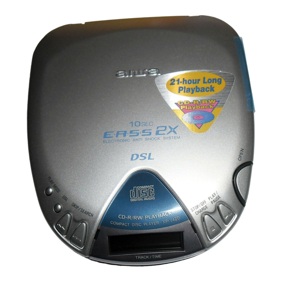
- Page 1 XP-V420 YJ1(S, LT),YHS1(S) XP-V421 AHC1(S,LL) AHRJ1(S,LT) SIMPLE-2 SERVICE MANUAL COMPACT DISC PLAYER BASIC CD MECHANISM : DA23LN A par t of contents is adequate. Re-issuing is under r equest. S/M Code No. 09-013-354-9N2...
-
Page 2: Specifications
SPECIFICATIONS 420YJ1 420YHS1 • Design and specifications are subject to change without notice • Design and specifications are subject to change without notice 421AHC1 421AHRJ1 • • Design and specifications are subject to change without Design and specifications are subject to change without notice notice... -
Page 3: Protection Of Eyes From Laser Beam During Servicing
PROTECTION OF EYES FROM LASER BEAM DURING SERVICING This set employs laser. Therefore, be sure to follow carefully the CAUTION instructions below when servicing. Use of controls or adjustments or performance of procedures other than those specified herein may result in hazardous WARNING! radiation exposure. -
Page 4: Pick Up Assy
Precaution to replace Optical block (SF-P200) Body or clothes electrostatic potential could ruin laser diode in the optical block. Be sure ground body and workbench, and use care the clothes do not touch the diode. 1) After the connection, remove solder shown in the right figure. - Page 5 ELECTRICAL MAIN PARTS LIST-1/2 REF. NO PART NO. KANRI DESCRIPTION REF. NO PART NO. KANRI DESCRIPTION C414 87-012-188-080 C-CAP,U 47P-50 CH C415 87-A10-260-080 C-CAP,U 0.1-16 K B 87-A21-082-040 C-IC,BA6655AFV C417 87-012-188-080 C-CAP,U 47P-50 CH 8A-HCH-603-010 C-IC,MN101C439-AE C418 87-012-176-080 CAP 15P 87-A21-446-010 C-IC,MN662782RPT1 C419...
- Page 6 ELECTRICAL MAIN PARTS LIST-2/2 REF. NO PART NO. KANRI DESCRIPTION REF. NO PART NO. KANRI DESCRIPTION L401 87-A50-711-080 C-COIL,47UH-LEMF3225 S303 87-A91-622-010 SW,MICRO PV1102 L402 87-A50-712-080 C-COIL,100UH-LEMF3225 S304 87-036-349-010 SW,TACT SKHHAJ L501 87-A50-367-080 C-COIL, 10UH LQG21F S305 87-036-349-010 SW,TACT SKHHAJ L502 87-A50-367-080 C-COIL, 10UH LQG21F S306...
- Page 7 TRANSISTOR ILLUSTRATION-1/1 B C E 2SA1162 IMH4A 2SB1132 2SC2412 2SD1664 2SC2712 CPH3106 CPH3206 DTC114EK DTC114TK DTC123JK RN2411...
- Page 8 FL (AHC-7) GRID ASSIGNMENT/ANODE CONNECTION-1/1...
- Page 9 WIRING-1/2 (MAIN: COMPONENT SIDE) MAIN C.B (COMPONENT SIDE) NOTE...
- Page 10 WIRING-2/2 (MAIN: CONDUCTOR SIDE) J701 MAIN C.B PHONES/LINE OUT (CONDUCTOR SIDE) VR701 S308 LIMIT CD OPTICAL PICKUP SPINDLE SLED S303 ASSY PLAY/ VR701 MOTOR MOTOR OPEN DA23LH PAUSE S309 STOP/OFF CHARGE D701 6 5 4 3 2 1 – J151 DC 5~6V D101 D702...
- Page 11 SCHEMATIC DIAGRAM-1/1 (MAIN) PHONES/ LINE OUT D701 100/6.3 C423 0.22 C511 220/6.3 C516 DAN202K SFPB52 D101 -11-...
- Page 12 TEST MODE-1/3 OPEN/CLOSE SW SHORT LAND S303 IC502 IC501 IC401 IC451 IC601 IC701 IC301 TEST MODE SHORT LAND -12-...
- Page 13 TEST MODE-2/3 The servo circuit of this model is designed to be adjustment-free and the adjustment value and disc distinction (CD-DA, CD-R and CD-RW) etc. is adjusted by the IC. Therefore the adjustment is performed at each TOC reading. The adjustment conditions in the IC of each servo can be monitored in this test mode.
- Page 14 TEST MODE-3/3 3. Confirmation of Sled movement By pressing the F.SKIP or B.SKIP button continuously during the TEST MODE, it is possible to transfer the pick-up to either the outer side or inner side. 4. Confirmation of the RF level Test point: RF and VC (Vref) Test disc: TCD-782 Confirm that the RF waveform is as shown below.
- Page 15 WAVE FORM-1/1 IC501 Pin 7 VOLT/DIV: 0.5V IC401 Pin VOLT/DIV: 2V TIME/DIV: 1µS TIME/DIV: 5µS f=44.1kHz IC501 Pin ∞ VOLT/DIV: 0.2V IC401 Pin ™ VOLT/DIV: 1V TIME/DIV: 50µS TIME/DIV: 5µS IC501 Pin ) VOLT/DIV: 0.1V TIME/DIV: 2mS IC401 Pin VOLT/DIV: 1V TIME/DIV: 50mS f=16.93MHz -15-...
- Page 16 IC BLOCK DIAGRAM-1/2 IC, BA6655AFV power off Ref.vol Vref2 Regulator Starter Starter Normal Ref.vol Vref1 Power Power switch 1 switch 2 ST PULSE Switching driver IC, AN8838NSB -16-...
- Page 17 IC BLOCK DIAGRAM-2/2 IC, AN8746SA IC, TA2120FN IC, MSM51V4400 TIMING GENERATOR TIMING GENERATOR WRITE COLUMN CLOCK COLUMN ADDRESS GENERATOR DECODERS BUFFERS OUTPUT BUFFERS INTERNAL REFRESH SENSE D0~D3 A0~A9 ADDRESS CONTROL CLOCK AMPLIFIERS SELECTOR COUNTER INPUT BUFFERS ADDRESS WORD MEMORY BUFFERS DRIVERS CELLS CODERS...
- Page 18 IC DESCRIPTION-1/2 (MN662782RPT1)-1/2 Pin No. Pin Name Description DVDD3 Power supply for DRAM interface. (pin No. 2 to 19). 2, 3 D0, 1 DRAM data input/output signal 0, 1. DRAM write enable signal. NRAS DRAM RAS control signal. 6, 7 D2, 3 DRAM data input/output signal 2, 3.
- Page 19 IC DESCRIPTION-1/2 (MN662782RPT1)-2/2 Pin No. Pin Name Description AVDD1 Power supply for analog circuit (for audio output block). FSEL Noise filter ON/OFF switching input. L: ON. H: OFF. 53, 54 TMOD1, 2 Terminal mode select input terminal 1, 2. Normal: L. FLAG Flag signal output.
- Page 20 IC DESCRIPTION-2/2 (MN101C439-AE)-1/2 Pin No. Pin Name Description COM3-0 LCD common. VLC3 — — VLC2 — — VLC1 — — — LCD power supply. OSC2 Microprocessor main clock oscillator output. (Not connected) OSC1 Microprocessor main clock oscillator input. — Ground. Sub-clock oscillator input.
- Page 21 IC DESCRIPTION-2/2 (MN101C439-AE)-2/2 Pin No. Pin Name Description DSL1 DSL ON control output of headphones. DSL ON= H. MUTE Audio mute output. STANDBY Standby output of headphones. During standby =L. Power on= H. LCDRDO Wired LCD remote control output. (Not connected) P-OFF Power-off output of power supply IC.
- Page 22 VOLTAGE CHART-1/2 THE MEASURED VALUE IS DC VOLTAGE CD SECTION TEST CONDITION:CD PLAY IC401 (MN662782RPT1 ) PIN'S NUMBER CD PLAY 2.88 1.44 1.47 2.88 2.67 1.44 1.46 2.69 2.88 0.60 PIN'S NUMBER CD PLAY 0.60 0.29 0.20 0.46 0.53 0.49 0.16 0.49 0.16...
- Page 23 VOLTAGE CHART-2/2 IC501 (AN8838NSB) PIN'S NUMBER CD PLAY 2.88 1.47 1.46 1.47 1.47 1.45 1.63 0.72 1.86 PIN'S NUMBER CD PLAY 1.77 1.95 2.83 1.49 1.47 PIN'S NUMBER CD PLAY 0.32 0.46 1.50 0.32 1.43 1.48 1.58 1.42 IC502 (NJU7012F) PIN'S NUMBER CD PLAY 1.43...
- Page 24 MECHANICAL EXPLODED VIEW-1/1 -24-...
- Page 25 MECHANICAL PARTS LIST-1/1 REF. NO PART NO. KANRI DESCRIPTION REF. NO PART NO. KANRI DESCRIPTION 1 88-HC6-021-010 FOOT, DIA10 14 8B-HCH-002-010 CABI,CENTER 420 S 2 8B-HCH-003-010 CABI,BOTTOM 420 S <420YJ1SC,420YHS1SC,421AHC1SCC,421AHRJ1SC> <420YJ1SC,420YHS1SC,421AHC1SCC,421AHRJ1SC> 14 8B-HCH-011-010 CABI,CENTER LL<421AHC1LLCC> 2 8B-HCH-071-010 CABI,BOTTOM L<421AHC1LLCC> 14 8B-HCH-009-010 CABI,CENTER SK<420YJ1LTC,421AHRJ1LTC>...
-
Page 26: Color Name Table
COLOR NAME TABLE Basic color symbol Color Basic color symbol Color Basic color symbol Color Black Cream Orange Green Gray Blue Transparent Blue Gold Pink Silver Titan Silver Brown Violet White Transparent White Yellow Transparent Yellow Metallic Blue Light Blue Transparent Green Dark Blue Transparent Orange... - Page 27 ACCESSORIES/PACKAGE LIST-1/1 REF. NO PART NO. KANRI DESCRIPTION 1 8B-HCH-903-010 IB,HC(ECC)C 421<421AHC1LLCC,421AHC1SCC> 1 8B-HCH-902-010 IB,HR(ECA)C 421<421AHRJ1SC,421AHRJ1LTC> 1 8B-HCH-913-010 IB,YHS(ECC)C 420<420YHS1SC> 1 8B-HCH-923-010 IB,YHS(K)S 420<420YHS1SC> 1 8B-HCH-912-010 IB,YJ(ECS)C 420<420YJ1SC,420YJ1LTC> 2 87-B30-286-010 AC ADAPTOR,AC-D603HCNC <421AHC1LLCC,421AHC1SCC> 3 87-B30-423-010 HEADPHONE,HP-M062 4 87-A91-017-010 PLUG,CONVERSION JT-0476 <421AHRJ1SC,421AHRJ1LTC>...
- Page 28 2–11, IKENOHATA 1–CHOME, TAITO-KU, TOKYO 110-8710, JAPAN TEL:03 (3827) 3111 H251941...
Need help?
Do you have a question about the XP-V420 and is the answer not in the manual?
Questions and answers