
Related Manuals for Aiwa XP-V320


Summary of Contents for Aiwa XP-V320
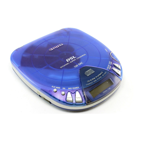
- Page 1 XP-V320 Y1(S,B) XP-V321 AEZ1(S) XP-V322 AEZ1(S) XP-V323 YL1(S,DT,YT,LT) SERVICE MANUAL COMPACT DISC PLAYER BASIC CD MECHANISM : DA23L S/M Code No. 09-013-354-8N1...
-
Page 2: Protection Of Eyes From Laser Beam During Servicing
PROTECTION OF EYES FROM LASER BEAM DURING SERVICING This set employs laser. Therefore, be sure to follow carefully the CAUTION instructions below when servicing. Use of controls or adjustments or performance of procedures other than those specified herein may result in hazardous WARNING! radiation exposure. -
Page 3: Pick Up Assy
Precaution to replace Optical block (SF-P200) Body or clothes electrostatic potential could ruin laser diode in the optical block. Be sure ground body and workbench, and use care the clothes do not touch the diode. 1) After the connection, remove solder shown in the right figure. -
Page 4: Specifications
SPECIFICATIONS XP-V320 XP-V321 • • Design and specifications are subject to change without Design and specifications are subject to change without notice notice XP-V322 XP-V323 • • Design and specifications are subject to change without Design and specifications are subject to change without... - Page 5 ELECTRICAL MAIN PARTS LIST-1/2 REF. NO PART NO. KANRI DESCRIPTION REF. NO PART NO. KANRI DESCRIPTION C354 87-010-831-080 C-CAP,U,0.1-16F C355 87-012-176-080 CAP 15P 87-A21-448-040 C-IC,BH6554FV C356 87-012-176-080 CAP 15P 87-A21-083-040 C-IC,BH6508FS C357 87-010-831-080 C-CAP,U,0.1-16F 87-A21-381-040 C-IC,LA9235M C358 87-012-195-080 C-CAP,U 100P-50CH 87-A21-591-010 C-IC,LC78641NE-D 87-A21-085-040...
- Page 6 ELECTRICAL MAIN PARTS LIST-2/2 REF. NO PART NO. KANRI DESCRIPTION S801 87-A91-622-010 SW,MICRO PV1102 S802 87-A91-742-010 SW,SL 4-1-3 HSW2061-010010 VR701 87-A92-167-010 VR,RTRY 30KCX2 H RK14J12A0-N X351 87-A70-202-080 C-VIB,CER 16.93MHZ CSACV-MXJ04 • Regarding connectors, they are not stocked as they are not the initial order items. The connectors are available after they are supplied from connector manufacturers upon the order is received.
- Page 7 TRANSISTOR ILLUSTRATION-1/1 B C E 2SA1037 2SB1132 2SK2980 2SC2412 2SD1664 CPH3106 DTC114TK DTC123JK...
- Page 8 FL (AHC-7) GRID ASSIGNMENT/ANODE CONNECTION-1/1...
- Page 9 WIRING-1/1...
- Page 10 SCHEMATIC DIAGRAM-1/1 6P 2HV 16P H Toc-A -10-...
- Page 11 TEST MODE-1/3 IC101 IC351 IC301 IC201 Q305 IC701 IC801 TEST MODE SHORT LAND -11-...
- Page 12 TEST MODE-2/3 The servo circuit of this model has been designed to be free of adjustments and controlled within the IC. Therefore, adjustments and disk judgement are performed automatically every time the TOC is read out. The adjustment status of each servo inside the IC can be monitored in this test mode. 1.
- Page 13 TEST MODE-3/3 4. Amount of change of jitter The amount of change of jitter is displayed in the focus bias check mode. The displayed value has 256 steps from 00 to FF. Example: focus bias (FB) Adjustment value™00 Jitter value™FD RNDM RESUME Focus bias...
- Page 14 WAVE FORM-1/1 IC301 Pin ≥ VOLT/DIV: 0.2V IC351 Pin ∞ VOLT/DIV: 0.1V TIME/DIV: 0.5µS SPDO TIME/DIV: 5mS IC301 Pin * VOLT/DIV: 0.2V TIME/DIV: 50µS IC301 Pin ¡ VOLT/DIV: 0.1V TIME/DIV: 2mS IC351 Pin VOLT/DIV: 1V XOUT TIME/DIV: 50mS f=16.93MHz IC801 Pin VOLT/DIV: 1V TIME/DIV: 0.2µS f=4.2MHz...
- Page 15 IC BLOCK DIAGRAM-1/1 IC, BH6508FS VREF MUTE IC, BH6554FV IC, TA2120FN I N - L I N - R -15-...
- Page 16 IC DESCRIPTION-1/3 (LC78641NE-D)-1/3 Pin No. Pin Name Description PDO1 Internal VCD control phase comparator output pin. PDO2 Internal VCD control phase comparator output pin. OFF for rough servo, ON for phase servo. VVSS — Internal VCD ground pin. PCKIST PDO output current adjustment resistor connection pin. (pull up) Internal VCD power supply pin.
- Page 17 IC DESCRIPTION-1/3 (LC78641NE-D)-2/3 Pin No. Pin Name Description DOUT Digital OUT output pin. (EIAJ format) (Not connected) Output pin for the 7.35kHz synchronization signal divided from the crystal osillator. (Not connected) EFLG (Not connected) TEST C1 C2 error correction monitor pin. Test input pin. Must be connected to OV. Emphasis pin.
- Page 18 IC DESCRIPTION-1/3 (LC78641NE-D)-3/3 Pin No. Pin Name Description Focus ON detect pin. Microprocessor interface power supply. (2000pF or more path controller to be inserted at a point VDD5V — nearer to the pin between this pin and GND) — Digital ground pin. Must be connected to 0V. CONT6 General-purpose input/output pin 6.
- Page 19 IC DESCRIPTION-2/3 (µPD789406AGC-014)-1/2 Pin No. Pin Name Description VDD1 — Positive polarity power supply (except for port section). BIAS — Feeding the LCD drive power supply voltage. VLC0-VLC2 — LCD drive power supply voltage. VSS1 — Ground potential (except for port section). 7-10 COM0-COM3 Common signal output from LCD controller/driver.
- Page 20 IC DESCRIPTION-2/3 (µPD789406AGC-014)-2/2 Pin No. Pin Name Description — Terminal to connect external crystal for main system clock oscillation. VSS0 — Ground potential of port section. VDD0 — Positive polarity power supply for port section. — Not connected. Terminal to connect external crystal for sub system clock oscillation. (Connected to Ground) IC/VPP —...
- Page 21 IC DESCRIPTION-3/3 (LA9235M)-1/1 Pin No. Pin Name Description FIN1 FIN2 Pick-up signal input. TIN1 TIN2 REF1 Pin designed for reference voltage. VREF Reference voltage output. APC monitor voltage input. APC output. — GND. LDOF Laser OFF pin. (H: ON L: OFF) ODRV Speed switch pin.
- Page 22 VOLTAGE CHART-1/2 THE MEASURED VALUE IS DC VOLTAGE TEST CONDITION:CD PLAY IC351 (LC78641NE) PIN'S NUMBER CD PLAY 1.23 0.93 3.02 2.28 0.01 1.57 1.50 1.50 PIN'S NUMBER CD PLAY 1.79 1.67 1.15 1.50 1.55 1.51 3.02 1.45 PIN'S NUMBER CD PLAY 1.50 1.55 1.60...
- Page 23 VOLTAGE CHART-2/2 IC101 (BH6554FV) PIN'S NUMBER CD PLAY 2.68 2.72 7.05 2.11 7.05 2.27 0.43 2.11 2.77 PIN'S NUMBER CD PLAY 0.15 0.36 3.04 3.04 0.01 3.04 0.38 1.19 PIN'S NUMBER CD PLAY 0.90 0.64 0.03 3.06 3.06 3.06 2.64 IC301 (LA9235M) PIN'S NUMBER CD PLAY...
- Page 24 MECHANICAL EXPLODED VIEW-1/1 DA23L -24-...
- Page 25 MECHANICAL PARTS LIST-1/1 REF. NO PART NO. KANRI DESCRIPTION REF. NO PART NO. KANRI DESCRIPTION 1 8B-HC7-007-010 KEY,SKIP 14 8B-HC7-082-010 CABI ASSY,BOTTOM 320 DT 2 8B-HC7-005-010 WINDOW,DISPLAY 320<320Y1SC,320Y1BSC> <323YL1DTCC,323YL1BDTCC> 2 8B-HC7-021-010 WINDOW,DISPLAY 321<321AEZ1SC> 14 8B-HC7-083-010 CABI ASSY,BOTTOM 320 LT 2 8B-HC7-022-010 WINDOW,DISPLAY 322<322AEZ1SC>...
-
Page 26: Color Name Table
COLOR NAME TABLE Basic color symbol Color Basic color symbol Color Basic color symbol Color Black Cream Orange Green Gray Blue Transparent Blue Gold Pink Silver Titan Silver Brown Violet White Transparent White Yellow Transparent Yellow Metallic Blue Light Blue Transparent Green Dark Blue Transparent Orange... - Page 27 CD MECHANISM EXPLODED VIEW-1/1 (DA23L) -27-...
- Page 28 CD MECHANISM PARTS LIST-1/1 (DA23L) REF. NO PART NO. KANRI DESCRIPTION 1 S0-A41-A20-600 PICKUP LASER ASSY 2 SM-10A-108-001 MOTOR ASSY SPINDLE 3 S0-M10-A10-900 MOTOR SLED ASSY 4 S2-311-A12-200 CHASSIS 5 S2-511-A23-200 GEAR MIDDLE 6 S2-511-A23-100 GEAR,SCREW 7 S2-511-A23-400 GEAR,RACK 8 S2-511-A07-900 SPINDLE SCREW 9 S4-S13-A00-200 SW,LEAF...
- Page 29 ACCESSORIES/PACKAGE LIST-1/1 REF. NO PART NO. KANRI DESCRIPTION 1 8B-HC7-915-010 IB,EZ(EGF)C 321<321AEZ1SC> 1 8B-HC7-905-010 IB,EZ(EGF)C 322<322AEZ1SC> 1 8B-HC7-917-010 IB,EZ(PHNCZ)C 321<321AEZ1SC> 1 8B-HC7-907-010 IB,EZ(PHNCZ)C 322<322AEZ1SC> 1 8B-HC7-916-010 IB,EZ(SID)C 321<321AEZ1SC> 1 8B-HC7-906-010 IB,EZ(SID)C 322<322AEZ1SC> 1 8B-HC7-925-010 IB,Y(EGF)C 320<320Y1SC,320Y1BSC> 1 8B-HC7-927-010 IB,Y(PHNCZ)C 320<320Y1SC,320Y1BSC> 1 8B-HC7-926-010 IB,Y(SID)C 320<320Y1SC,320Y1BSC>...
- Page 30 2–11, IKENOHATA 1–CHOME, TAITO-KU, TOKYO 110-8710, JAPAN TEL:03 (3827) 3111 H251701 Printed in Singapore...
Need help?
Do you have a question about the XP-V320 and is the answer not in the manual?
Questions and answers