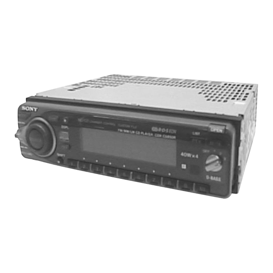
Sony CDX-C5850R Service Manual
Fm/mw/lw compact disc player
Hide thumbs
Also See for CDX-C5850R:
- Operating instructions manual (124 pages) ,
- Service manual (54 pages) ,
- Installation/connections (4 pages)
Table of Contents
Advertisement
Quick Links
SERVICE MANUAL
CD player section
System
Compact disc digital audio
system
Signal-to-noise ratio
90 dB
Frequency response
10 – 20,000 Hz
Wow and flutter
Below measurable limit
Tuner section
FM
Tuning range
87.5 – 108.0 MHz
Aerial terminal
External aerial connector
Intermediate frequency 10.7 MHz
Usable sensitivity
12 dBf
Selectivity
75 dB at 400 kHz
Signal-to-noise ratio
65 dB (stereo),
68 dB (mono)
Harmonic distortion at 1 kHz
0.8% (stereo),
0.6% (mono)
Separation
35 dB at 1 kHz
Frequency response
30 – 15,000 Hz
MW/LW
Tuning range
MW: 531 – 1,602 kHz
LW: 153 – 281 kHz
Aerial terminal
External aerial connector
Intermediate frequency 10.7 MHz / 450 kHz
MW: 30 µV
Sensitivity
LW: 50 µV
MICROFILM
CDX-C5850R
Model Name Using Similar Mechanism
CD Drive Mechanism Type
Optical Pick-up Name
SPECIFICATIONS
Power amplifier section
Outputs
Speaker impedance
Maximum power output 40 W × 4 (at 4 ohms)
General
Outputs
Tone controls
Power requirements
Dimensions
Mounting dimension
Mass
Supplied accessories
Design and specifications are subject to change without
notice.
FM/MW/LW COMPACT DISC PLAYER
– 1 –
AEP Model
UK Model
CDX-C570R/C580R
MG-363T-121
KSS-521A
Speaker outputs
(sure seal connectors)
4 – 8 ohms
Line outputs (2)
Power aerial relay control
lead
Power amplifier control
lead
Telephone ATT control
lead
Bass ±8 dB at 100 Hz
Treble ±8 dB at 10 kHz
12 V DC car battery
(negative ground)
Approx. 178 × 50 × 185 mm
(w/h/d)
Approx. 182 × 53 × 162 mm
(w/h/d)
Approx. 1.2 kg
Parts for installation and
connections (1 set)
Front panel case (1)
Advertisement
Table of Contents

Related Manuals for Sony CDX-C5850R


Summary of Contents for Sony CDX-C5850R
- Page 1 CDX-C5850R SERVICE MANUAL AEP Model UK Model Model Name Using Similar Mechanism CDX-C570R/C580R CD Drive Mechanism Type MG-363T-121 Optical Pick-up Name KSS-521A SPECIFICATIONS CD player section Power amplifier section System Compact disc digital audio Outputs Speaker outputs system (sure seal connectors)
- Page 2 COMPONENTS IDENTIFIED BY MARK ! OR DOTTED LINE WITH MARK ! ON THE SCHEMATIC DIAGRAMS AND IN THE PARTS LIST ARE CRITICAL TO SAFE OPERATION. REPLACE THESE COMPONENTS WITH SONY PARTS WHOSE PART NUMBERS APPEAR AS SHOWN IN THIS MANUAL OR IN SUPPLEMENTS PUBLISHED BY SONY.
-
Page 3: Table Of Contents
TABLE OF CONTENTS 1. GENERAL Location of controls ..............4 Getting Started ................. 4 Setting the clock ..............4 CD Player ................5 Radio ..................5 RDS ..................6 Other Functions ............... 7 CD/MD Unit ................8 Connections ................10 2. - Page 4 SECTION 1 GENERAL This section is extracted from instruction manual. – 4 –...
- Page 5 – 5 –...
- Page 6 – 6 –...
- Page 7 – 7 –...
- Page 8 – 8 –...
- Page 9 – 9 –...
- Page 10 – 10 –...
- Page 11 – 11 –...
-
Page 12: Cover
SECTION 2 DISASSEMBLY Note : Follow the disassembly procedure in the numerical order given. 2-1. COVER 1 claw 4 cover 3 claws 2 claw 2-2. FRONT PANEL ASSY 3 Push the bearing (L). 2 Push the bearing (R). 4 front panel assy 1 Push the button (open). -
Page 13: Sub Panel Assy
2-3. SUB PANEL ASSY 4 claws 6 CNP800 2 PTT 2.6x6 5 claw 1 PTT 2.6x6 7 sub panel assy 3 PTT 2.6x6 2-4. CD MECHANISM BLOCK 2 PTT 2.6x6 5 PTT 2.6x6 7 bracket (M/D) 1 PTT 2.6x6 4 CD mechanism block 6 PTT 2.6x6 3 CNP700 –... -
Page 14: Main Board
2-5. MAIN BOARD 6 MAIN board 4 ground point screws (PTT 2.6x6) 5 ground point screw (PTT 2.6x6) 3 PTT 2.6x8 2 PTT 2.6x8 1 PTT 2.6x8 2-6. HEAT SINK 5 heat sink 4 PTT 2.6x8 3 PTT 2.6x8 2 PTT 2.6x12 1 PTT 2.6x8 –... -
Page 15: Chassis (T) Sub Assy
2-7. CHASSIS (T) SUB ASSY 5 chassis (T) sub assy 1 P 2x3 2 P 2x3 3 P 2x3 4 claw 2-8. LEVER ASSY 5 guide (disc) 6 lever (R) assy 3 tension spring (LR) 7 lever (L) assy 1 PS 2x4 2 DISC IN SW board 4 claws –... -
Page 16: Servo Board
2-9. SERVO BOARD 6 PS 2x4 5 PS 2x4 2 CN2 1 CN3 3 P 2x3 7 SERVO board 4 loading motor assy 2-10. ROLLER ASSY • When installing, take note of the positions arm (roller) and washers. (Fig. 1) washer arm washer washers Fig. -
Page 17: Chassis (Op) (O/S) Assy
2-11. CHASSIS (OP) (O/S) ASSY 7 chassis (OP) (O/S) assy 8 compression spring (FL) 1 tension spring (angle) 9 compression spring (FL) 2 tension spring (KR1) 5 Fit lever (D) in the direction of the arrow. 6 Turn loading ring in the direction of the arrow. -
Page 18: Electrical Adjustments
SECTION 3 ELECTRICAL ADJUSTMENTS 0 dB = 1 µV FM Auto Scan/Stop Level Adjustment TUNER SECTION Setting : D-BASS switch : OFF Cautions during repair SOURCE button : FM When the tuner unit is defective, replace it by a new one because its internal block is difficult to repair. - Page 19 FM Stereo Separation Adjustment FM RDS S-Meter Adjustment Setting : Setting : D-BASS switch : OFF D-BASS switch : OFF SOURCE button : FM SOURCE button : FM FM RF signal FM RF signal generator generator level meter antenna antenna terminal 10 k Ω...
- Page 20 MW Auto Scan/Stop Level Adjustment Adjustment Location : tuner unit (TU601) Setting : D-BASS switch : OFF SOURCE n MODE button : MW 30 Ω 15 pF 65 pF AM RF signal generator AM dummy antenna (50 Ω ) TU601 antenna Carrier frequency : 999 kHz terminal...
-
Page 21: Cd Section
Focus Gain Adjustment (Coarse adjustment) CD SECTION This adjustment is not required unless the following parts are replaced: • Optical pick-up Note: • 1. CD Block basically constructed to operate without adjustment. Therefore, check each item in order given. Procedure: 2. -
Page 22: Diagrams
SECTION 4 DIAGRAMS 4-1. IC PIN DESCRIPTION • IC801 MB90574APMT-G-200-BND (SYSTEM CONTROL) Pin No. Pin Name Pin Description LD ON Laser ON/OFF control output Focus OK signal detection input XLAT25 CD signal processing latch output DATA25 CD signal serial data output XRST Reset output to CD signal processor IC. - Page 23 Pin No. Pin Name Pin Description Pin No. Pin Name Pin Description AMP ON Power amplifier power control output ANT REM ANT REMOTE power control output TXT ON Reset output to CD-TEXT decoder IC. — Not used. (Open) VOL ATT Electric volume mute control output CTL2 —...
-
Page 24: Block Diagram -Cd Section
CDX-C5850R 4-2. BLOCK DIAGRAM — CD SECTION — OPTICAL PICK-UP RF AMP, SERVO CONTROL DIGITAL SIGNAL PROESSOR D/A CONVERTER KSS-521A IC702 RF 0 PCMD V OUTL CD L-CH TUNER SECTION BCKIN R-CH CLKO V OUTR (Page 27) XLTO LRCK LRCIN... -
Page 25: Block Diagram -Tuner Section
CDX-C5850R 4-3. BLOCK DIAGRAM — TUNER SECTION — PJ400 –1 ELECTRONIC R-CH (Page 26) BUS AUDIO IN VOLUME IC401 –2 PJ400 –3 SECTION OUT FL FRONT –4 TUNER UNIT CD L-CH R-CH MUTE TU601 Q110 LINE OUT CNJ600 ANT AM (ANTENNA) –5... -
Page 26: Block Diagram -Display Section
CDX-C5850R 4-4. BLOCK DIAGRAM — DISPLAY SECTION — SYSTEM CONTROL LCD DRIVE IC801 (3/3) IC501 RESET RESET DATA BU5V IC902 LCD501 S900 RESET COLOR GREEN 2 SELECT LED501-505 Q504 S901 LSW512-521, (NOSE DET) COLOR LSW531-538 72 NOSE2 AMBER 3 SELECT... -
Page 27: Circuit Boards Location
• Waveforms (MODE:PLAY) 4-5. CIRCUIT BOARDS LOCATION THIS NOTE IS COMMON FOR PRINTED WIRING BOARDS AND SCHEMATIC DIAGRAMS. (In addition to this, the necessary note is printed in each block.) for schematic diagram: DISC IN SW board • All capacitors are in µF unless otherwise noted. pF: µµF Approx. -
Page 28: Printed Wiring Boards -Cd Mechanism Section
CDX-C5850R 4-6. PRINTED WIRING BOARDS — CD MECHANISM SECTION — • Semiconductor Location Ref. No. Location (Page 39) M902 M901 (SLED) (SPINDLE) – 33 – – 34 –... -
Page 29: Schematic Diagram -Cd Mechanism Section
CDX-C5850R 4-7. SCHEMATIC DIAGRAM — CD MECHANISM SECTION — • Refer to page 32 for Waveforms. • Refer to page 53 for IC Block Diagrams. Note: • Voltage and waveforms are dc with respect to ground under no-signal conditions. no mark : CD PLAY ∗... -
Page 30: Printed Wiring Board -Main Section
CDX-C5850R 4-8. PRINTED WIRING BOARD — MAIN SECTION — • Semiconductor Location Ref. No. Location Ref. No. Location (D402) IC401 D403 IC601 (D404) IC602 IC603 (D405) (D406) (IC702) F-11 (D407) IC703 IC801 (D408) (D409) IC803 D-14 (D410) (IC901) F-13 (IC902) - Page 31 CDX-C5850R (Page 33) (Page 48) – 39 – – 40 –...
-
Page 32: Schematic Diagram -Main Section (1/3)
CDX-C5850R 4-9. SCHEMATIC DIAGRAM — MAIN SECTION (1/3) — • Refer to page 55 for IC Block Diagrams. Note: (Page 44) (Page 45) • Voltage is dc with respect to ground under no-signal (detuned) condition. no mark : FM ) : MW <... -
Page 33: Schematic Diagram -Main Section (2/3)
CDX-C5850R 4-10. SCHEMATIC DIAGRAM — MAIN SECTION (2/3) — • Refer to page 53 for IC Block Diagrams. (Page 41) Note: • Voltage is dc with respect to ground under no-signal (detuned) condition. no mark : FM ) : MW <... -
Page 34: Schematic Diagram -Main Section (3/3)
CDX-C5850R 4-11. SCHEMATIC DIAGRAM — MAIN SECTION (3/3) — • Refer to page 55 for IC Block Diagrams. 4-12. SCHEMATIC DIAGRAM — RELAY SECTION — (Page 42) (Page 51) Note: • Voltage is dc with respect to ground under no-signal (detuned) condition. -
Page 35: Printed Wiring Board -Relay Section
CDX-C5850R 4-13. PRINTED WIRING BOARD — RELAY SECTION — (Page 39) (Page 50) – 47 – – 48 –... -
Page 36: Printed Wiring Board -Display Section
CDX-C5850R 4-14. PRINTED WIRING BOARD — DISPLAY SECTION — • Semiconductor Location Ref. No. Location Ref. No. Location D501 C-12 (LED502) A-2 (Page 48) D502 (LED503) B-1 D503 C-12 (LED504) C-2 D505 B-10 (LED505) C-3 D506 B-10 LED510 D507 B-10... -
Page 37: Schematic Diagram -Display Section
CDX-C5850R 4-15. SCHEMATIC DIAGRAM — DISPLAY SECTION — (Page 46) Note: • Voltage is dc with respect to ground under no-signal (detuned) condition. no mark : FM – 51 – – 52 –... - Page 38 IC2 CXA1782BQ • IC Block Diagrams IC1 CXD2507AQ IC602 SAA6588T-118 27 26 25 IIC-BUS PSWN SLAVE TRANSCEIVER SERVO AUTO SEQUENCER DATA SIGNAL PAUSE INTERFACE QUALITY DETECTOR REGISTER XRST AFIN DETECTOR SENS SUB CODE MUTE PROCESSOR INTERFACE LEVEL S DAVN SQCK CLOCKED RDS/RDBS RDS/RDBS...
- Page 39 IC401 TDA7462 SE3L SE3R MUTE PAUSE PAUSE DETECT FRONT INPUT TREBLE/ OUT FL LOUDNESS VOICE BANDPASS VOLUME FADER GAIN & SOFT BASS CONTROL CONTROL SE1L AUTO MUTE CONTROL CIRCUIT CIRCUIT SE1R ZERO CIRCUIT FRONT MD– OUT FR FADER CDL+ CDL– COMPANDER CDR–...
- Page 40 IC601 TDA7427AD1TR LPOUT VDD1 VDD2 LP FM SWITCH CHARGE PHASE 11 BIT PROG LP1/LP2 GND AM PUMP COMP COUNTER LP HC LP AM SWITCH SWITCH SWM/DIR SWM/DIR V REF AM IN SWITCH AM/FM INLOCK 6 BIT PROG PRE COUNTER DETECTOR COUNTER :32/33 FM IN...
-
Page 41: Exploded Views
SECTION 5 EXPLODED VIEWS NOTE: • The mechanical parts with no reference • Color Indication of Appearance Parts The components identified by number in the exploded views are not supplied. Example : mark ! or dotted line with mark. • Items marked “*” are not stocked since ! are critical for safety. -
Page 42: Front Panel Section
5-2. FRONT PANEL SECTION not supplied (DISPLAY board) LCD501 Ref. No. Part No. Description Remark Ref. No. Part No. Description Remark 3-030-944-01 LEVER (SEEK/AMS) 3-030-901-01 RING 3-030-950-01 BUTTON (OPEN) * 61 3-030-888-01 PLATE (LCD), GROUND 3-032-321-01 SPRING (OPEN) * 62 3-032-199-01 SHEET (ESD) X-3376-753-1 PANEL ASSY, FRONT * 63... -
Page 43: Cd Mechanism Section (1)
5-3. CD MECHANISM SECTION (1) (MG-363T-121) M903 Ref. No. Part No. Description Remark Ref. No. Part No. Description Remark * 101 1-659-836-11 DISC IN SW BOARD 3-931-902-04 ARM (ROLLER) * 102 A-3291-816-B CHASSIS (T) SUB ASSY 3-936-756-01 ROLLER (D) 3-931-909-01 SPRING (LR), TENSION 3-321-393-01 WASHER, STOPPER X-3371-501-1 LEVER (L) ASSY * 113... -
Page 44: Cd Mechanism Section (2)
5-4. CD MECHANISM SECTION (2) (MG-363T-121) Ref. No. Part No. Description Remark Ref. No. Part No. Description Remark 3-931-893-01 ARM, CHUCKING A-3277-802-C CHASSIS (M) ASSY 3-931-897-01 DAMPER (T) 3-931-883-01 SPRING (TR), TENSION 3-931-879-02 LEVER (D) 3-931-881-01 LEVER (LOCK) * 154 3-913-404-11 RETAINER (DISC) 3-931-882-02 GEAR (MDL) 3-931-894-01 BRACKET (CP) -
Page 45: Cd Mechanism Section (3)
5-5. CD MECHANISM SECTION (3) (MG-363T-121) M901 M902 The components identified by mark ! or dotted line with mark. ! are critical for safety. Replace only with part number specified. Ref. No. Part No. Description Remark Ref. No. Part No. Description Remark * 201... -
Page 46: Electrical Parts List
SECTION 6 DISC IN SW DISPLAY ELECTRICAL PARTS LIST NOTE: • Due to standardization, replacements in • Items marked “*” are not stocked since The components identified by the parts list may be different from the they are seldom required for routine service. mark ! or dotted line with mark. - Page 47 DISPLAY LIMIT SW LOAD SW MAIN Ref. No. Part No. Description Remark Ref. No. Part No. Description Remark R531 1-216-043-00 RES,CHIP 1/10W 1-659-837-11 LOAD SW BOARD R532 1-216-045-00 METAL CHIP 1/10W *************** R533 1-216-045-00 METAL CHIP 1/10W R534 1-216-049-11 RES,CHIP 1/10W <...
- Page 48 MAIN Ref. No. Part No. Description Remark Ref. No. Part No. Description Remark C417 1-124-234-00 ELECT 22uF C663 1-163-037-11 CERAMIC CHIP 0.022uF C499 1-164-346-11 CERAMIC CHIP C664 1-164-004-11 CERAMIC CHIP 0.1uF C601 1-163-235-11 CERAMIC CHIP 22PF C665 1-164-004-11 CERAMIC CHIP 0.1uF C602 1-164-182-11 CERAMIC CHIP...
- Page 49 MAIN Ref. No. Part No. Description Remark Ref. No. Part No. Description Remark CNP802 1-566-822-41 JACK (REMOTE IN) D916 8-719-921-80 DIODE MTZJ-11B D918 8-719-914-44 DIODE DAP202K < CONNECTOR > D919 8-719-914-43 DIODE DAN202K D920 8-719-978-69 DIODE DTZ-TT11-16B CNP501 1-774-701-11 PIN, CONNECTOR 16P D924 8-719-200-82 DIODE 11ES2 CNP700 1-764-617-12 PIN, CONNECTOR (PC BOARD) 30P...
- Page 50 MAIN Ref. No. Part No. Description Remark Ref. No. Part No. Description Remark < JACK > R115 1-216-075-00 METAL CHIP 1/10W R116 1-216-075-00 METAL CHIP 1/10W PJ400 1-774-700-21 JACK, PIN 6P (BUS AUDIO IN,LINE OUT) R117 1-216-129-00 METAL CHIP 2.2M 1/10W R118 1-216-129-00 METAL CHIP...
- Page 51 MAIN Ref. No. Part No. Description Remark Ref. No. Part No. Description Remark R627 1-216-113-00 METAL CHIP 470K 1/10W R830 1-216-073-00 METAL CHIP 1/10W R628 1-216-057-00 METAL CHIP 2.2K 1/10W R831 1-216-073-00 METAL CHIP 1/10W R630 1-216-097-00 RES,CHIP 100K 1/10W R832 1-216-097-00 RES,CHIP 100K...
- Page 52 MAIN RELAY SERVO Ref. No. Part No. Description Remark Ref. No. Part No. Description Remark < SWITCH > 1-163-021-11 CERAMIC CHIP 0.01uF 1-163-989-11 CERAMIC CHIP 0.033uF S900 1-692-431-21 SWITCH, TACTILE (RESET) 1-164-004-11 CERAMIC CHIP 0.1uF S901 1-571-754-31 SWITCH, PUSH (1 KEY) (NOSE DET) 1-164-004-11 CERAMIC CHIP 0.1uF 1-163-037-11 CERAMIC CHIP...
- Page 53 SERVO Ref. No. Part No. Description Remark Ref. No. Part No. Description Remark JR17 1-216-296-00 SHORT JR71 1-216-296-00 SHORT JR18 1-216-296-00 SHORT JR19 1-216-296-00 SHORT < COIL > JR20 1-216-296-00 SHORT JR21 1-216-296-00 SHORT 1-412-058-11 INDUCTOR CHIP 10uH 1-412-058-11 INDUCTOR CHIP 10uH JR22 1-216-296-00 SHORT 1-412-058-11 INDUCTOR CHIP 10uH...
- Page 54 CDX-C5850R SERVO Ref. No. Part No. Description Remark Ref. No. Part No. Description Remark 1-216-107-00 METAL CHIP 270K 1/10W ACCESSORIES & PACKING MATERIALS 1-216-097-00 RES,CHIP 100K 1/10W ******************************** 1-216-085-00 METAL CHIP 1/10W 1-216-081-00 METAL CHIP 1/10W 3-865-875-11 MANUAL, INSTRUCTION, INSTALL (ENGLISH,...
Need help?
Do you have a question about the CDX-C5850R and is the answer not in the manual?
Questions and answers