
Related Manuals for Motorola 880


Summary of Contents for Motorola 880
- Page 1 GSM/DCS 880/890 DualBand Cellular Subsciber Group The Worlds Leading Cellular Telephone Manufacturer Service Manual...
- Page 2 The Motorola products described in this instruction manual may include copy- righted Motorola computer programs stored in semi-conductor memories or other media. Laws in the United States and other countries preserve for Motorola certain exclusive rights for copyrighted computer programs, including the exclusive right to copy or reproduce in any form the copyrighted computer program.
-
Page 3: Preface
PREFACE Dual Band 880/890 (DCS/GSM) Cellular Subscriber Sector Preface Specifications Table 1: General Function GSM Specification DCS 1800 Specification Frequency Range 890-915 MHz TX 1710-1785 MHz TX 935-960 MHz RX 1805-1880 MHz RX Channel Spacing 200 kHz Channels 124 carriers with 8 channels per carrier... - Page 4 Dual Band 880/890 (DCS/GSM) Table 2: Transmitter Function Specification Spurious Emissions -36 dBm up to 1 GHz, (<-30 dBm > 1 GHz) Table 3: Receiver Function Specification RF Level -102 dBm RX bit error rate (100 k bits) < 2%...
-
Page 5: Foreword
Motorola maintains a parts office staffed to process parts orders, identify part numbers, and otherwise assist in the maintenance and repair of Motorola Cellular products. Orders for all parts should be sent to the Motorola International Logis- tics Department at the following address:... -
Page 6: General Safety Information
Dual Band 880/890 (DCS/GSM) General Safety Information Portable Operation DO NOT hold the radio so that the antenna DO NOT operate this equipment near elec- is very close to, or touching, exposed parts trical blasting caps or in an explosive atmo- of the body, especially the face or eyes, while sphere. -
Page 7: Table Of Contents
Testing ......15 Dual Band 880 Mechnical ....59 Dual Band 880 Electrical RF/Logic . - Page 8 Replacement Trouble- Personality Identity and Theory of Glossary Parts shooting Disassembly Transfer Testing Security Operation Description...
-
Page 9: Description
SIM card, the mute and volume button This rechargeable Lithium Ion battery contacts and magnetic reed switch. pack is the lightest Motorola battery offered for the phone. It measures 9.4mm The RF/Logic board consists of the Audio/ thick, and gives approximately 58-75... - Page 10 Dual Band 880/890 (DCS/GSM) • Slim Battery NiCad (SNN4132) The battery charger plugs into the This rechargeable Nickel Cadmium accessory connector socket, situated at the battery pack measures 9.4mm thick, and base of the telephone, and a vehicle’s cigar gives approximately 33 hours standby.
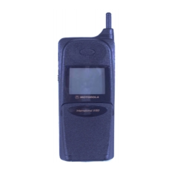
- Page 11 Description Figure 1: Dual Band 880/890 Personal Cellular Telephone Retractable Antenna Earpiece Mute Button Volume Buttons SIM Eject Button Keypad 2 x 12 Digit Display Flip Microphone 12/9/97 68P09403A50...
-
Page 12: Key / Unique Features (Knifeswitch)
• Advice of Charge Enhancement: Added • Lens & Nameplate Color Differentiation: number of digits for currencies. The Dual Band 880 will have white printing on a black background. (GSM • GSM Voicemail Icon: Voicemail Icon GC-87 / 8700 phones are gold on black, or... -
Page 13: Feature List
Description • 9600 Baud Data / Fax: The product provides Memories: up to 9600 baud data for the fastest available Phone - numbered memory 100 transfer of faxes and data. SIM card - dependent on SIM • Phase 2 Features: The product provides Last 10 numbers dialed other GSM phase 2 features including: Last 10 numbers received (if using CLI) -
Page 14: Key / Unique Features Dual Band 890
Dual Band 880/890 (DCS/GSM) Home rate or Roam rate Key / Unique Features Dual Band 890 (Band Aware) Call restrictions levels: Restrict keypad dialing / incoming calls / The GCSA Dual Band 890 operates in GSM number length 900 and DCS 1800 bands and utilizes phased PIN entry / enable/disable / change /unblock signalling. -
Page 15: Theory Of Operation
THEORY OF OPERATION Dual Band 880/890 (DCS/GSM) Cellular Subscriber Sector Theory of Operation GSM System Overview Using this technique, radiation on a given channel is virtually contained in the cell operating on that channel and, to some extent, those cells directly adjacent to that cell. - Page 16 Dual Band 880/890 (DCS/GSM) It is designed to carry digital voice and The radiotelephones themselves are capable data over existing copper telephone of operation on any channel in the system, cables. The GSM phone will be able to allowing them to operate in any cell. Due to...
- Page 17 Theory of Operation The data blocks are modulated onto the Signal information provides an indication of carrier using Gaussian Minimum Shift the subscriber’s distance from the base Keying (GMSK), a very efficient method of station. As the radiotelephone moves from phase modulation.
- Page 18 Dual Band 880/890 (DCS/GSM) 68P09403A50 12/9/97...
-
Page 19: Identity And Security
Transceiver Labelling the sections shown below. Introduction Figure 5: IMEI Configuration Each Motorola GSM transceiver will be labelled with various number configura- IMEI 15 digits tions. The following information shows and 6 digits... -
Page 20: Sim Cards
Dual Band 880/890 (DCS/GSM) Ensure that the contacts of the card face SIM CARDS towards the front of the phone (i.e. towards the flip). Introduction The Motorola GSM 8700/6700 personal The sliding, card release button will move cellular telephones are designed to work upwards as the SIM card is inserted. - Page 21 Identity and Security To protect the actual unit from unauthorized use, a lock function on the hardware is avail- able. When enabled, this function requires that a three or four digit unlock code be entered, via the units keypad, before normal operation of the transceiver can take place.
- Page 22 Dual Band 880/890 (DCS/GSM) 68P09403A50 12/9/97...
-
Page 23: Testing
TESTING Dual Band 880/890 (DCS/GSM) Cellular Subscriber Sector Testing GSM Verification Equipment Configuration Initially insert the test SIM card into the slot Introduction at the rear of the personal cellular telephone. If required, further information on SIM card To test the phone cellular telephone for func- insertion is available on page 12. -
Page 24: Gsm Manual Test Mode
Dual Band 880/890 (DCS/GSM) Figure 7: GSM Testing Configuration Unit To Be Tested GSM Compatible Communications Analyzer RF In/out Port Test Adaptor (SKN4683A or SMA Connector SKN4665A) (Not Connected) Plugs into accessory connector of phone. GSM Manual Test Mode and securely into the slot at the base of the phone. - Page 25 Testing indicating that the unit is now in the Manual Accessing The Manual Test Mode Test Mode. Table 5: “GSM Test Commands” on page 17 shows the available Manual Test When the Test SIM card is in place, power commands their corresponding up the telephone.
- Page 26 Dual Band 880/890 (DCS/GSM) Table 5: GSM Test Commands Key Sequence Test Function/Name Deactivate SIM Initiate sending all 1’s Initiate sending all 0’s Disable echo processing 43x# Change audio path 45xxx# Serving cell power level Display current value of AFC DAC...
-
Page 27: Dcs Manual Test Mode
Testing DCS Manual Test Mode Accessing The Manual Test Mode Introduction When the Test SIM card is in place, power up the telephone. Once the initial automatic The phones are equipped with a Manual ‘wake up’ sequence has taken place Test Mode capability. - Page 28 Dual Band 880/890 (DCS/GSM) Table 6: DCS Test Commands Table 6: DCS Test Commands Test Function/Name Test Function/Name Sequence Sequence 24x# Set step AGC 66xyyy# Display/modify TMSI 25xxx# Set continuous AGC Zero PLMN Selector 26xxxx# Set continuous AFC Zero forbidden PLMN list...
-
Page 29: Dcs Verification Testing
Testing DCS Verification Testing Figure 8: DCS Verification Testing Equipment Setup SMA CONNECTOR D.C.S. COMPATIBLE COMMUNICATIONS ANALYSER ANTENNA TEST ADAPTOR (0109354C01) RF IN/OUT PORT MENU UNIT TO BE TESTED (WITH BATTERY FITTED) 12/9/97 68P09403A50... - Page 30 Dual Band 880/890 (DCS/GSM) Introduction Testing Procedure To test a telephone, to verify whether or not All information required to perform the the unit is functioning correctly, the desired tests and measurements, should be following equipment will be required: obtained from the communication analy zer’s user manual.
- Page 31 Testing Table 7: Test and Tolerances Test To Be Performed Lower Limit Upper Limit Transmit average phase error (RMS) at max and min power Transmit average phase error (Peak) at max and min power Transmit average frequency error at max and min power -90 Hz +90 Hz Transmit power error at level 7 (29 dBm) on CH62...
- Page 32 Dual Band 880/890 (DCS/GSM) 68P09403A50 12/9/97...
-
Page 33: Personality Transfer
PERSONALITY TRANSFER Dual Band 880/890 (DCS/GSM) Cellular Subscriber Sector Personality Transfer cloning mode, and ready to transfer the first block of data. Step 3. Enter 021# via the units keypad. Introduction This command will cause the first block information Due to the different variations (OEM looks) uploaded into the Transfer card. -
Page 34: Master Transfer
Step 5. When the data block has been power up, or complete a Normal Transfer. transferred successfully, remove As mentioned earlier, there are different the Master Transfer card and check variations (OEM looks) of the Motorola repaired radio functions GSM 8700/6700 cellular telephones, each correctly. -
Page 35: Master Sim Card Creation
Personality Transfer Master SIM Card Creation When required a Master SIM card can be created by: Step 1. Insert a Transfer card into a unit which is already configured in the desired way. Turn the unit on, the display should show ‘Clone’. Step 2. - Page 36 Dual Band 880/890 (DCS/GSM) 68P09403A50 12/9/97...
-
Page 37: Disassembly
DISASSEMBLY Dual Band 880/890 (DCS/GSM) Cellular Subscriber Sector Disassembly Introduction Recommended Tools Before disassembly is started, the antenna The following tools are recommended for connector cap at the top of the phone has to use during the disassembly and reassembly be removed to allow full separation. - Page 38 Dual Band 880/890 (DCS/GSM) Antenna Removal Step 1. Turn off the telephone. Step 2. Press down on the battery’s tab, slide down, and remove battery from housing. Step 3. Carefully antenna cap using a plastic pry tool. Step 4. Remove...
- Page 39 Disassembly Board Removal Step 1. The front housing, con- training all the internal circuitry, can now be lifted away. Step 2. Unclip the microphone plug using a plastic pry tool. Step 3. Carefully ease the Logic/RF board away from Keypad/Display board, which connects to it via a 41 pin plug/socket connector.
- Page 40 Dual Band 880/890 (DCS/GSM) Step 4. The Logic/RF board can now be removed completely from the front housing. Step 5. Carefully unclip the plastic slider plate, starting from the opposite side to the SIM card eject button. Step 6. Pry...
- Page 41 Disassembly Flip Removal Step 1. To remove the flip, hold it fully open to expose the two slots on the shaft. Using a dental pick, locate the small holes on the hinge cams. Push hinge cam in turn towards the center of the flip while easing the flip outwards.
- Page 42 Dual Band 880/890 (DCS/GSM) 68P09403A50 12/9/97...
-
Page 43: Troubleshooting
TROUBLESHOOTING Dual Band 880/890 (DCS/GSM) Cellular Subscriber Sector Troubleshooting Introduction If the Logic/RF assembly is replaced a personality transfer will be necessary. See “Personality Transfer” on page 25. Assembly replacement level trouble- shooting and repair of the phone is limited... - Page 44 Dual Band 880/890 (DCS/GSM) Table 6: GSM Receiver Troubleshooting and Repair Chart RX Symptom Probable Cause Verification and Remedy Portable tele- Antenna assembly is 1. Check to make sure that the antenna pins phone exhibits defective. are properly connected to the Logic/RF poor reception assembly.
- Page 45 Troubleshooting Table 6: GSM Receiver Troubleshooting and Repair Chart RX Symptom Probable Cause Verification and Remedy Receive audio Antenna assembly is 1. Check to make sure antenna pin is properly is weak and/or defective. connected Logic/RF Board distorted. Assembly. If OK, substitute a known good antenna assembly.
- Page 46 Dual Band 880/890 (DCS/GSM) Table 8: GSM Logic/Processing Troubleshooting and Repair Chart Logic/Processing Probable Cause Verification and Remedy Symptom 1. Unit Doesn’t a) Battery either discharged or 1. Measure battery voltage across a 50 ohm Turn On or defective. (>1 Watt) load.
- Page 47 Troubleshooting Table 8: GSM Logic/Processing Troubleshooting and Repair Chart Logic/Processing Probable Cause Verification and Remedy Symptom 1. Unit Doesn’t c) Defective RF/Audio-Logic 1. Gain access to Keypad/Display / main Turn On or Board assembly. board as described in “Disassembly” on Stay On page 29.
- Page 48 Dual Band 880/890 (DCS/GSM) Table 8: GSM Logic/Processing Troubleshooting and Repair Chart Logic/Processing Probable Cause Verification and Remedy Symptom Display is Logic/RF Board Assembly 1. Substitute known good Logic/RF erratic, or defective. Assembly. provides 2. If known assembly works, the original is...
- Page 49 Troubleshooting Table 8: GSM Logic/Processing Troubleshooting and Repair Chart Logic/Processing Probable Cause Verification and Remedy Symptom Phone will not SIM card defective 1. Initially check that the contacts on the card recognize/ are not dirty; clean if necessary, and check accept SIM if fault has been eliminated.
- Page 50 Dual Band 880/890 (DCS/GSM) Table 8: GSM Logic/Processing Troubleshooting and Repair Chart Logic/Processing Probable Cause Verification and Remedy Symptom Hinged mouth- Magnet in flip defective. 1. Replace flip assembly with known good piece does one. not go on/off 2. Place call to portable phone and verify hook correctly.
-
Page 51: Troubleshooting Supplements
Troubleshooting Troubleshooting Supplements Logic/Processing Supplement 1 - Unit Doesn’t Power Up (NPU) START Apply power to the radio. Is 6.5V dc Proceed to “#1 NPU Repair Procedure” on page 46. present at U900 pin 40? Press the power key to initiate PCB power up process. - Page 52 Dual Band 880/890 (DCS/GSM) Is +2.75V present Proceed to “#5 NPU Repair Procedure” on page 48. at U701 pins 45, 46, 58, and 59? Does U900 pin 30 Proceed to “#6 NPU Repair Procedure” on page 48. reset line go high?
- Page 53 Troubleshooting Is CS signalling Proceed to “#9 NPU Repair Procedure” on page 49. present at U702 at pins 39 and 40? Is OE+ signalling Proceed to “#10 NPU Repair Procedure” on page 49. present at U705 pin 1? Radio is resetting - Proceed to “#11 NPU Repair Procedure”...
- Page 54 Dual Band 880/890 (DCS/GSM) #1 NPU Repair Procedure No +6.5V dc battery supply voltage present at pin 40 of U900. • Check the PCB battery contact assembly for dry joints to the PCB, or broken contacts. Resolder any dry joints, or replace the battery contact assembly if any of the contacts are broken.
- Page 55 If no supply voltage to the chip, trace its B+ path and/or replace the chip. If after replacing all of the above components the fault is not eliminated, return the PCB to a Motorola Hi Tech Center. 12/9/97 68P09403A50...
- Page 56 • Check that U900 is not physically damaged, has no dry joints, and is positioned correctly. If none of the mentioned problems are apparent replace U900. If replacing U900 the fault is still apparent return PCB to a Motorola Hi Tech Center. #7 NPU Repair Procedure The watchdog line at pin 31 of U900 does not go high to +2.75V dc.
- Page 57 If none of the mentioned problems are apparent, replace U704 and U705. If replacing the above components does not eliminate the fault, return the PCB to a Motorola Hi Tech Center. #9 NPU Repair Procedure No signalling present at pins 39 and 40 of U702.
- Page 58 Dual Band 880/890 (DCS/GSM) #11 NPU Repair Procedure Radio is resetting. If the radio executes external device communication and then powers itself down very shortly after attempting power up, it is resetting. A reset can be caused by a fault on either U703, U500, or U701.
- Page 59 Troubleshooting Logic/Processing Supplement 3 - Phone Failure “See Supplier” Display shows phone failure, see supplier Apply power to the unit and enter Test Mode. Press 7100# Read the return code. INFO 00 05 INFO 00 03 INFO 00 07 Perform a master cloning. - Replace Speech Replace Modem IC Coder U500...
- Page 60 • Y702 • CR221 • All chips If the above analysis does not identify the fault, return the PCB to a Motorola Hi Tech Center. Logic/Processing Supplement 5 - PCB Draws Current When Off • Ensure that the +6.5V power supply is being applied to the PCB , and that the PCB is switched off.
-
Page 61: Introduction
Troubleshooting Introduction DCS Testing After Repair Assembly replacement level trouble- After any repair work has been carried out, shooting and repair of the phone is limited the unit should be thoroughly tested to to those components listed in the Replace- ensure that its operates correctly. - Page 62 Dual Band 880/890 (DCS/GSM) Table 7: DCS Receiver Troubleshooting and Repair Chart RX Symptom Probable Cause Verification and Remedy Portable tele- Antenna assembly is 1. Check to make sure that the antenna pins phone exhibits defective. are properly connected to the Logic/RF poor reception assembly.
- Page 63 Troubleshooting Table 7: DCS Receiver Troubleshooting and Repair Chart RX Symptom Probable Cause Verification and Remedy Receive audio Antenna assembly is 1. Check to make sure antenna pin is properly is weak and/or defective. connected Logic/RF Board distorted. Assembly. If OK, substitute a known good antenna assembly.
- Page 64 Dual Band 880/890 (DCS/GSM) 68P09403A50 12/9/97...
- Page 65 Troubleshooting Figure 9: RF Block Diagram 12/9/97 68P09403A50...
- Page 66 Dual Band 880/890 (DCS/GSM) Figure 10: GSM Dual BandFunctional Block Diagram 68P09403A50 12/9/97...
-
Page 67: Replacement Parts
Cellular Subscriber Sector Replacement Parts Dual Band 880 Mechnical Transceiver: SWF2622A Model Description: Dual Band 880 The following tables are the Replacement Parts lists for the following Dual Band 880 Schematic Reference: 8409468S01 models: 1997-09-19 Model No. Model Name S7028ABB Hong Kong *Not pictured. - Page 68 Dual Band 880/890 (DCS/GSM) ITEM # DESCRIPTION 4009203D01 SW KYPD METAL DOMES 4009203D02 SW ARRAY KYPD METAL DOMES 4009608M03 SWITCH SMT CARD RDR PRESENCE 4082635T09 SWITCH REED SMD 16-20AT 4109083R02 SPRING COMPRESSION 4209190E01 CLIP LOGIC SHIELD #2 4209935N01 CLIP DESENSE...
-
Page 69: Dual Band 880 Electrical Rf/Logic
Replacement Parts Dual Band 880 Electrical RF/Logic ITEM # DESCRIPTION C00207 2113743L41 CAP CHIP 10000 PF ITEM # DESCRIPTION 10% X7R A00002 3909014B02 CONTACT ANTENNA C00208 2113743N17 CAP CHIP 4.3 PF +- RECEPTACLE .25PF COG C00102 2311049A54 CAP TAN CHIP A/P 3.3... - Page 70 Dual Band 880/890 (DCS/GSM) ITEM # DESCRIPTION ITEM # DESCRIPTION C00235 2113743N50 CAP CHIP 100 PF 5% C00264 2311049A56 CAP TAN CHIP A/P 4.7 20 10 C00236 2113743L17 CAP CHIP 1000 PF 10% C00265 2113743N34 CAP CHIP 22.0 PF 5% C00237 2113743N26 CAP CHIP 10.0 PF 5%...
- Page 71 Replacement Parts ITEM # DESCRIPTION ITEM # DESCRIPTION C00320 2113743N01 CAP CHIP 0.5 PF +- C00353 2113743N20 CAP CHIP 5.6 PF + -.5PF .25PF COG C00321 2113743N07 CAP CHIP 1.5 PF +- C00354 2113743N02 CAP CHIP 0.75 PF +- .25PF COG .25PF COG C00322 2113743N03 CAP CHIP 1.0 PF +-...
- Page 72 Dual Band 880/890 (DCS/GSM) ITEM # DESCRIPTION ITEM # DESCRIPTION C00418 2113743N26 CAP CHIP 10.0 PF 5% C00529 2113741F49 CAP CHIP CL2 X7R REEL 10000 C00430 2113741F49 CAP CHIP CL2 X7R C00530 2113740F55 CAP CHIP REEL CL1 +/- REEL 10000...
- Page 73 Replacement Parts ITEM # DESCRIPTION ITEM # DESCRIPTION C00712 2113743E07 CER CHIP CAP .022UF C00813 2113740F39 CAP CHIP REEL CL1 +/- 30 33 C00714 2113741F25 CAP CHIP CL2 X7R REEL 1000 C00815 2113743E07 CER CHIP CAP .022UF C00750 2113743E12 CAP CHIP .047 UF 10% C00816 2113743E20 CAP CHIP .10 UF 10% C00817...
- Page 74 Dual Band 880/890 (DCS/GSM) ITEM # DESCRIPTION ITEM # DESCRIPTION C00901 2113743H14 CAP CHIP 10.0 UF 16V CR0221 4809641F04 DIODE VCTR SMV1204- +80-20% 70 SOT23 C00902 2113743H14 CAP CHIP 10.0 UF 16V CR0223 4809948D05 DIODE RF SWITCH SMT +80-20% SOD323 C00903 2113743H14 CAP CHIP 10.0 UF 16V...
- Page 75 Replacement Parts ITEM # DESCRIPTION ITEM # DESCRIPTION FL0400 9109450C01 FLTR SAW 947.5 MHZ L00460 2409646M0 IND CER MULTILYR 8.2NH 1608 FL0401 9109111C08 FLTR CER 1800 MHZ L00461 2409646M1 IND CER MULTILYR 27NH 1608 FL0460 9109179E01 FLTR SAW PB 215MHZ 150KHZ BW L00462 2409646M0...
- Page 76 Dual Band 880/890 (DCS/GSM) ITEM # DESCRIPTION ITEM # DESCRIPTION Q00222 4809579E18 TSTR MOSFET P-CHAN Q00804 4809940E02 TSTR DIG NPN TP0101T DTC114YE Q00300 4809605E02 TSTR SIG NPN 2SC4617 Q00905 4809607E02 TSTR SIG PNP 25A1774 Q00301 4809579E04 TSTR MOSFET P-CHAN Q00906...
- Page 77 Replacement Parts ITEM # DESCRIPTION ITEM # DESCRIPTION R00210 0662057M7 RES. CHIP 1500 5% R00241 0662057N07 RES. CHIP 22K 5% 20X40 20X40 R00211 0662057M7 RES. CHIP 1000 5% R00242 0662057M9 RES. CHIP 10K 5% 20X40 20X40 R00212 0662057M7 RES. CHIP 1500 5% R00243 0662057M8 RES.
- Page 78 Dual Band 880/890 (DCS/GSM) ITEM # DESCRIPTION ITEM # DESCRIPTION R00337 0662057M2 RES. CHIP 10 5% R00430 0662057M5 RES. CHIP 150 5% 20X40 20X40 R00340 0660076N73 RES CHIP 10 K OHM 1/ R00431 0662057M9 RES. CHIP 4700 5% 16 W...
- Page 79 Replacement Parts ITEM # DESCRIPTION ITEM # DESCRIPTION R00527 0660076N13 RES CHIP 33 OHM 5 1/ R00711 0660076N77 RES CHIP 15 K OHM 1/ 16 W R00601 0660076N80 RES CHIP 20 K OHM 1/ R00712 0660076N77 RES CHIP 15 K OHM 1/ 16 W 16 W R00602...
- Page 80 Dual Band 880/890 (DCS/GSM) ITEM # DESCRIPTION ITEM # DESCRIPTION R00745 0660076P01 RES CHIP 100K OHM 5 R00818 0660076S01 RES CHIP O OHM 1/16W R00822 0660076N01 RES CHIP 10 OHM 5 1/ R00746 0660076N77 RES CHIP 15 K OHM 1/...
- Page 81 Replacement Parts ITEM # DESCRIPTION ITEM # DESCRIPTION R00915 0660076N13 RES CHIP 33 OHM 5 1/ U00702 5199245A01 IC FLASH PROM 512KX16 28F800-B R00916 0660076N33 RES CHIP 220 OHM 1/16 U00703 5109743E13 IC ASIC BIC 4.01 S38138EC10 R00920 0660076N49 RES CHIP 1000 OHM 1/ U00704 5109509A06 IC SRAM 64KX16 16 W...
-
Page 82: Dual Band 880/890 Keyboard
Dual Band 880/890 (DCS/GSM) Dual Band 880/890 Keyboard ITEM # DESCRIPTION R01514 0660076P01 RES CHIP 100K OHM 5 ITEM # DESCRIPTION 1/16W C01501 2113743E12 CAP CHIP .047 UF 10% R01515 0660076N77 RES CHIP 15 K OHM 1/ 16 W C01502... -
Page 83: Dual Band 890 Electrical Rf/Logic
Replacement Parts Dual Band 890 Electrical RF/Logic ITEM # DESCRIPTION 0909883L04 RECP SMD LOW PRO 41 PIN ITEM # DESCRIPTION 0909888M01 RECEPT XDCR SMD 0909958J11 RECEP 10 PINS W/BATT W/COAX A00001 3909014B03 CONTACT ANTENNA 1009798H02 SOLDER PELLET 30X60 RECEPTACLE 1109012S01 PROTECTIVE TAPE LENS A00002 3909014B03... - Page 84 Dual Band 880/890 (DCS/GSM) ITEM # DESCRIPTION ITEM # DESCRIPTION C00203 2113743L17 CAP CHIP 1000 PF 10% C00232 2113743L41 CAP CHIP 10000 PF 10% C00205 2113743N50 CAP CHIP 100 PF 5% C00233 2113743L17 CAP CHIP 1000 PF 10% C00206 2113743N18 CAP CHIP 4.7 PF +-...
- Page 85 Replacement Parts ITEM # DESCRIPTION ITEM # DESCRIPTION C00261 2113743N50 CAP CHIP 100 PF 5% C00315 2113740L05 CAP CER CHIP 3.0 PF +- 0.1PF C00262 2113743L17 CAP CHIP 1000 PF 10% C00317 2113743N01 CAP CHIP 0.5 PF +- .25PF COG C00263 2113743M24 CAP CHIP 100000 PF...
- Page 86 Dual Band 880/890 (DCS/GSM) ITEM # DESCRIPTION ITEM # DESCRIPTION C00351 2113743L17 CAP CHIP 1000 PF 10% C00413 2113743N30 CAP CHIP 15.0 PF 5% C00352 2113743L17 CAP CHIP 1000 PF 10% C00415 2113743L41 CAP CHIP 10000 PF 10% C00353 2113743N18 CAP CHIP 4.7 PF +-...
- Page 87 Replacement Parts ITEM # DESCRIPTION ITEM # DESCRIPTION C00523 2113743E20 CAP CHIP .10 UF 10% C00708 2113743E12 CAP CHIP .047 UF 10% C00524 2113740F55 CAP CHIP REEL CL1 +/- 30 150 C00709 2113743E07 CER CHIP CAP .022UF C00525 2113743E20 CAP CHIP .10 UF 10% C00710 2113740F55 CAP CHIP REEL CL1 +/-...
- Page 88 Dual Band 880/890 (DCS/GSM) ITEM # DESCRIPTION ITEM # DESCRIPTION C00810 2113743A27 CAP CHIP .470 UF 10% C00859 2113740F39 CAP CHIP REEL CL1 +/- 30 33 C00811 2113740F39 CAP CHIP REEL CL1 +/- C00889 2113740F39 CAP CHIP REEL CL1 +/-...
- Page 89 Replacement Parts ITEM # DESCRIPTION ITEM # DESCRIPTION CL0100 3909043M01 CNTCT ANT STRAW CR0704 4809606E01 DIODE ULTRA HIGH GRND SPEED UMT PKG CR0200 4809948D05 DIODE RF SWITCH CR0901 4813825A05 DIODE 30V HOT SMT SOD323 CARRIER MMBD301L CR0201 4809948D05 DIODE RF SWITCH CR0907 4809606E04 DIODE DUAL SW SMT SOD323...
- Page 90 Dual Band 880/890 (DCS/GSM) ITEM # DESCRIPTION ITEM # DESCRIPTION L00303 2409594M11 IND CHIP 15.0NH 5% Q00106 4809608E03 TSTR DIG PNP ACCU-L DTA114YE L00350 2409646M04 IND CER MULTILYR Q00107 4813823A07 XSTR N-CH TMOS FET 6.8NH 1608 2N7002LT1 L00378 2462587Q36 IND CHIP 120 NH 10%...
- Page 91 Replacement Parts ITEM # DESCRIPTION ITEM # DESCRIPTION Q00604 4813823A07 XSTR N-CH TMOS FET R00204 0662057M90 RES. CHIP 4700 5% 2N7002LT1 20X40 Q00605 4813823A07 XSTR N-CH TMOS FET R00205 0662057M86 RES. CHIP 3300 5% 2N7002LT1 20X40 Q00606 4809605E02 TSTR SIG NPN 2SC4617 R00206 0662057M54 RES.
- Page 92 Dual Band 880/890 (DCS/GSM) ITEM # DESCRIPTION ITEM # DESCRIPTION R00232 0662057M98 RES. CHIP 10K 5% R00333 0662057M43 RES. CHIP 51 5% 20X40 20X40 R00233 0662057M38 RES CHIP 33 5% 20X40 R00334 0662057M54 RES. CHIP 150 5% 20X40 R00234 0662057M84 RES.
- Page 93 Replacement Parts ITEM # DESCRIPTION ITEM # DESCRIPTION R00379 0660076P25 REC CHIP 1M OHN 5 1/ R00517 0660076N77 RES CHIP 15 K OHM 1/ 16 W R00380 0660076P25 REC CHIP 1M OHN 5 1/ R00518 0660076N77 RES CHIP 15 K OHM 1/ 16 W R00381 0662057M50...
- Page 94 Dual Band 880/890 (DCS/GSM) ITEM # DESCRIPTION ITEM # DESCRIPTION R00617 0660076P01 RES CHIP 100K OHM 5 R00736 0660076N77 RES CHIP 15 K OHM 1/ 1/16W 16 W R00619 0660076P25 REC CHIP 1M OHN 5 1/ R00737 0660076N77 RES CHIP 15 K OHM 1/...
- Page 95 Replacement Parts ITEM # DESCRIPTION ITEM # DESCRIPTION R00802 0660076N73 RES CHIP 10 K OHM 1/ R00842 0660076N69 RES CHIP 6800 OHM 1/ 16 W 16 W R00803 0660076N73 RES CHIP 10 K OHM 1/ R00843 0660076N69 RES CHIP 6800 OHM 1/ 16 W 16 W R00804...
- Page 96 Dual Band 880/890 (DCS/GSM) ITEM # DESCRIPTION ITEM # DESCRIPTION SH0009 2609280J02 SHIELD PA DUAL BAND U00901 4209935N01 CLIP DESENSE SOLID U00902 4209935N01 CLIP DESENSE T00900 2509021J01 CHOKE MEGA SHLDED VR0352 4809877C07 DIODE VARACTOR 47UH SMD SMV1104-35 U00101 5109920D12 IC DC-DC CONV...
- Page 97 Replacement Parts Figure 11 Mechanical Explosion Illustration 12/9/97 68P09403A50...
- Page 98 Dual Band 880/890 (DCS/GSM) 68P09403A50 12/9/97...
-
Page 99: Glossary
GLOSSARY Dual Band 880/890 (DCS/GSM) Cellular Subscriber Sector Glossary Those marked ** are Motorola specific abbreviations. BCCH Allocation A Interface Interface between MSC and BAIC Barring of All Incoming Calls BAOC Barring of all Outgoing Calls Authentication algorithm Base Transceiver Station (BTS) - Page 100 Dual Band 880/890 (DCS/GSM) Base Transceiver Station DISC DISConnect Data Link (layer) Control Channel (ISDN terminology applied to mobile Call Allocation service) CBCH Call Broadcast CHannel Signalling channel Call Control Dialled Pulse Country Code DRCU Diversity Radio Channel CCBS Completion of Calls to Busy...
- Page 101 Glossary Information (frames) FACCH Fast Associated Control CHannel International Alphanumeric 5 FACCH/F Full rate Fast Associated IDentification Control CHannel IMEI International Mobile FACCH/H Half rate Fast Associated Equipment Identity Control CHannel IMMediate assignment Frequency correction Burst message FCCH Frequency Correction IMSI International Mobile CHannel...
- Page 102 Dual Band 880/890 (DCS/GSM) Location Register MT/PP Mobile Terminated Point to Point messages Mobile Allocation Normal Burst Mobile Access Hunting Network Elements Mobile Allocation Index Norme European de MAIO Mobile Allocation Index Offset Telecommunications Mobile Application Part Network Management Mobile Country Code...
- Page 103 Glossary PSPDN Public Switched Packet Data Network PSTN Public Switched Telephone SABM Set Asynchronous Balance Model Public Telecommunications Operator SACCH Slow Associated Control CHannel SAPI Service Access Point Indicator (Identifier) Quality of Service Synchronization Burst Service Center SCCP Signalling Connection Control Part Random Access Burst Synchronization CHannel...
- Page 104 Dual Band 880/890 (DCS/GSM) Terminal Adaptor Unnumbered Information frame Timing Advance Air Interface TCAP Transaction Capabilities Application Part Traffic CHannel TCH/F A full rate TCH TCH/FS A full rate speech TCH Voice Activity Detection TCH/HS A half rate speech TCH...
- Page 105 2. Fill out the boxes below and give your comments. (This comment page can be used for any Motorola Cellular Subscriber service manual). 3. Fax this form to Motorola Greater China and South Asia Cellular Subscriber Division. Fax number (847) 523-8796, Attn: Mr. Derek Fung.
- Page 106 12/9/97...
- Page 107 XFMR 240 UK MT FAST GSM SPN4463A XT US FAST CHARGER BASE SWF2533C XCVR MERCURY 8800 C SYN6459A ESC GCSA DUAL BAND 880 Part Number Description ( for S7050AAB) SJN7300A USER MAN DB890 ENGLISH SNN4612B BATT GP4 FLEX NIMH BLK...
- Page 108 Greater China Cellular Subscriber Division Product Service Preview Dual Band 880/890 1309432S04 ESC LOGO MOT GOLD Set Up : Description: 1. The housing and the dimension is same as GSM 8700 2. There are 2 wiring coils in the Antenna insertion .
- Page 109 Distributors : Spare boards of DB880 is available; DB890 is not available until October of 97. Motorola HTCs :Schematics, layouts, L1 and L3 parts lists are available at Error! Bookmark not defined.. Please contact Error! Bookmark not defined. for any inquires.
- Page 147 Tx IF LO U220 GIFSYN IC 5109632D92 7100 # Display Error Code 512-Low 1710 1805 1590 U300 5109908K18 U340 PAC IC 5109632D08 700-Middle 1747,8 1842,8 1627,8 U370 TIC IC 5109632D94 Y201 Ref Clock Varactor 4809612J19 885-High 1785 1880 1665 Motorola Confidential Proprietary...
- Page 148 GSM_DCS Frequencys GSM / CHANNEL MAIN VCO Rx I.F Rx IF LO Tx I.F Tx IF LO 1-Low 890.2 935.2 720.2 62-Middle 902.4 947.4 732.4 124-High 914.8 959.8 744.8 DCS / CHANNEL MAIN VCO Rx I.F Rx IF LO Tx I.F Tx IF LO 512-Low 1710...
- Page 149 GSM_DCS Frequencys GSM / CHANNEL MAIN VCO Rx I.F Rx IF LO Tx I.F Tx IF LO 1-Low 890.2 935.2 720.2 62-Middle 902.4 947.4 732.4 124-High 914.8 959.8 744.8 DCS / CHANNEL MAIN VCO Rx I.F Rx IF LO Tx I.F Tx IF LO 512-Low 1710...
- Page 150 GSM_DCS Frequencys GSM / CHANNEL MAIN VCO Rx I.F Rx IF LO Tx I.F Tx IF LO 1-Low 890.2 935.2 720.2 62-Middle 902.4 947.4 732.4 124-High 914.8 959.8 744.8 DCS / CHANNEL MAIN VCO Rx I.F Rx IF LO Tx I.F Tx IF LO 512-Low 1710...
- Page 151 GSM_DCS Frequencys GSM / CHANNEL MAIN VCO Rx I.F Rx IF LO Tx I.F Tx IF LO 1-Low 890.2 935.2 720.2 62-Middle 902.4 947.4 732.4 124-High 914.8 959.8 744.8 DCS / CHANNEL MAIN VCO Rx I.F Rx IF LO Tx I.F Tx IF LO 512-Low 1710...
- Page 152 GSM_DCS Frequencys GSM / CHANNEL MAIN VCO Rx I.F Rx IF LO Tx I.F Tx IF LO 1-Low 890.2 935.2 720.2 62-Middle 902.4 947.4 732.4 124-High 914.8 959.8 744.8 DCS / CHANNEL MAIN VCO Rx I.F Rx IF LO Tx I.F Tx IF LO 512-Low 1710...
- Page 153 GSM_DCS Frequencys GSM / CHANNEL MAIN VCO Rx I.F Rx IF LO Tx I.F Tx IF LO 1-Low 890.2 935.2 720.2 62-Middle 902.4 947.4 732.4 124-High 914.8 959.8 744.8 DCS / CHANNEL MAIN VCO Rx I.F Rx IF LO Tx I.F Tx IF LO 512-Low 1710...
- Page 154 GSM_DCS Frequencys GSM / CHANNEL MAIN VCO Rx I.F Rx IF LO Tx I.F Tx IF LO 1-Low 890.2 935.2 720.2 62-Middle 902.4 947.4 732.4 124-High 914.8 959.8 744.8 DCS / CHANNEL MAIN VCO Rx I.F Rx IF LO Tx I.F Tx IF LO 512-Low 1710...
- Page 155 GSM_DCS Frequencys GSM / CHANNEL LAIN VCO Rx I.F Rx IF LO Tx I.F Tx IF LO 1-Low 890.2 935.2 720.2 62-Middle 902.4 947.4 732.4 124-High 914.8 959.8 744.8 DCS / CHANNEL LAIN VCO Rx I.F Rx IF LO Tx I.F Tx IF LO 512-Low 1710...
- Page 156 DUAL BAND 8800 / 8900 GSM_DCS Switch Matrix *GSM_DCS SW_RX_275 GSM_DCS MATRIX from CPU LOGIC_GSM_*DCS Q105 Q106 TX_GSM_*DCS GSM_*DCS Q115 SW_RX_275 SW_RX_275 GSM_RX275 Q114 TX_EN *GSM_DCS from CPU Q102 LOGIC_GSM_*DCS Q101 RX_EN RX275 Q103 FILTERED -10V from CPU DCS_RX275 LOGIC_GSM_*DCS Q113 REVISIONS Europe Middle East &...
- Page 157 DUAL BAND 8800 / 8900 GSM_DCS Switch Matrix *GSM_DCS SW_RX_275 GSM_DCS MATRIX from CPU LOGIC_GSM_*DCS Q105 Q106 TX_GSM_*DCS GSM_*DCS Q115 SW_RX_275 SW_RX_275 GSM_RX275 Q114 TX_EN *GSM_DCS from CPU Q102 LOGIC_GSM_*DCS Q101 RX_EN RX275 Q103 FILTERED -10V from CPU DCS_RX275 LOGIC_GSM_*DCS Q113 REVISIONS Europe Middle East &...
- Page 158 DUAL BAND 8800 / 8900 GSM_DCS Switch Matrix *GSM_DCS SW_RX_275 GSM_DCS MATRIX from CPU LOGIC_GSM_*DCS Q105 Q106 TX_GSM_*DCS GSM_*DCS Q115 SW_RX_275 SW_RX_275 GSM_RX275 Q114 TX_EN *GSM_DCS from CPU Q102 LOGIC_GSM_*DCS Q101 RX_EN RX275 Q103 FILTERED -10V from CPU DCS_RX275 LOGIC_GSM_*DCS Q113 REVISIONS Europe Middle East &...
- Page 159 DUAL BAND 8800 / 8900 GSM_DCS Switch Matrix *GSM_DCS SW_RX_275 GSM_DCS MATRIX from CPU LOGIC_GSM_*DCS Q105 Q106 TX_GSM_*DCS GSM_*DCS Q115 SW_RX_275 SW_RX_275 GSM_RX275 Q114 TX_EN *GSM_DCS from CPU Q102 LOGIC_GSM_*DCS Q101 RX_EN RX275 Q103 FILTERED -10V from CPU DCS_RX275 LOGIC_GSM_*DCS Q113 REVISIONS Europe Middle East &...
- Page 160 DUAL BAND 8800 / 8900 GSM_DCS Switch Matrix *GSM_DCS SW_RX_275 GSM_DCS MATRIX from CPU LOGIC_GSM_*DCS Q105 Q106 TX_GSM_*DCS GSM_*DCS Q115 SW_RX_275 SW_RX_275 GSM_RX275 Q114 TX_EN *GSM_DCS from CPU Q102 LOGIC_GSM_*DCS Q101 RX_EN RX275 Q103 FILTERED -10V from CPU DCS_RX275 LOGIC_GSM_*DCS Q113 REVISIONS Europe Middle East &...
- Page 161 DUAL BAND 8800 / 8900 GSM_DCS Switch Matrix *GSM_DCS SW_RX_275 GSM_DCS MATRIX from CPU LOGIC_GSM_*DCS Q105 Q106 TX_GSM_*DCS GSM_*DCS Q115 SW_RX_275 SW_RX_275 GSM_RX275 Q114 TX_EN *GSM_DCS from CPU Q102 LOGIC_GSM_*DCS Q101 RX_EN RX275 Q103 FILTERED -10V from CPU DCS_RX275 LOGIC_GSM_*DCS Q113 REVISIONS Europe Middle East &...
- Page 162 DUAL BAND 8800 / 8900 GSM_DCS Switch Matrix *GSM_DCS SW_RX_275 GSM_DCS MATRIX from CPU LOGIC_GSM_*DCS Q105 Q106 TX_GSM_*DCS GSM_*DCS Q115 SW_RX_275 SW_RX_275 GSM_RX275 Q114 TX_EN *GSM_DCS from CPU Q102 LOGIC_GSM_*DCS Q101 RX_EN RX275 Q103 FILTERED -10V from CPU DCS_RX275 LOGIC_GSM_*DCS Q113 REVISIONS Europe Middle East &...
- Page 163 Page 1 DUAL BAND 8800 / 8900_P16...
- Page 164 DUAL BAND 8800 / 8900 Improve Lock Time and Time Mask FIX Reference ECN: NS - 6176 Change R227 to 0662057M36 Add C343 - 2113740F23 Change C208 to 2113743N20 Change C208 to 2113743N12 Change R218 to 0662057M43 Change R206 to 0662057M50 Remove C337 C206 R206...
- Page 165 DUAL BAND 8800 / 8900 Improve Lock Time and Time Mask FIX Reference ECN: NS - 6176 Change R227 to 0662057M36 Add C343 - 2113740F23 Change C208 to 2113743N20 Change C208 to 2113743N12 Change R218 to 0662057M43 Change R206 to 0662057M50 Remove C337 C206 R206...
- Page 166 DUAL BAND 8800 / 8900 Improve Lock Time and Time Mask FIX Reference ECN: NS - 6176 Change R227 to 0662057M36 Add C343 - 2113740F23 Change C208 to 2113743N20 Change C208 to 2113743N12 Change R218 to 0662057M43 Change R206 to 0662057M50 Remove C337 C206 R206...
- Page 167 DUAL BAND 8800 / 8900 Improve Lock Time and Time Mask FIX Reference ECN: NS - 6176 Change R227 to 0662057M36 Add C343 - 2113740F23 Change C208 to 2113743N20 Change C208 to 2113743N12 Change R218 to 0662057M43 Change R206 to 0662057M50 Remove C337 C206 R206...
- Page 168 DUAL BAND 8800 / 8900 Improve Lock Time and Time Mask FIX Reference ECN: NS - 6176 Change R227 to 0662057M36 Add C343 - 2113740F23 Change C208 to 2113743N20 Change C208 to 2113743N12 Change R218 to 0662057M43 Change R206 to 0662057M50 Remove C337 C206 R206...
- Page 169 DUAL BAND 8800 / 8900 Voltage Supply Block Diagram from External Devices EXT_B+ from Battery VR901 BATT+ Q999 CR998 Q906 Q905 U900 GCAP B+ DC/DC Vswitch DC/DC Boost Mode Circuitry C916 Q301 CR910 VRef to GIFSYN 5.6V VSWITCH Q221 Q222 U220 GIFSYN Q100...
Need help?
Do you have a question about the 880 and is the answer not in the manual?
Questions and answers