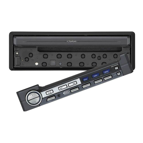
Clarion VRX765VD Service Manual
Dvd multmedia station with touch
panel controller
Hide thumbs
Also See for VRX765VD:
- Mode d'emploi et manuel d'installation (78 pages) ,
- Owners & installation manual (75 pages)
Table of Contents
Advertisement
Quick Links
SPECIFICATIONS
FM tuner section
Frequency range:
87.9MHz to 107.9MHz(B-A)
87.0MHz to 108.0MHz(K-A,B,C)
Usable sensitivity:
9dBf
50dB quieting sensitivity:
15dBf
Alternate channel selectivity:
70dB
Stereo separation:
35dB(1kHz)
Frequency response:
30Hz to 15kHz(+3/-3dB)
AM tuner section
Frequency range:
530kHz to 1710kHz(B-A)
531kHz to 1629kHz(K-A,B,C)
Usable sensitivity:
28dBu
DVD player section
System:
Digital versatile disc system with
CDDA capable
Usable discs:
DVD video disc,Compact disc
Frequency response:
20Hz to 20kHz(CD)(+1/-1dB)
Dynamic range:
100dB(1kHz)
Distortion:
0.01%
Clarion Co., Ltd.
50 Kamitoda, Toda-shi, Saitama 335-8511 Japan
Service Dept.: 5-66 Azuma , Kitamoto-shi, Saitama 364-0007 Japan
Tel: +81-48-541-2335 / 2432 FAX: +81-48-541-2703
Service Manual
- 1 -
DVD Multmedia Station with Touch
Panel Controller
Model
(QC-6823B-A)
(NTSC/ Region No. "1")
Model
(QC-6823K-A)
(PAL/ Region No. "3")
Model
(QC-6823K-B)
(NTSC/ Region No. "3")
Model
(QC-6823K-C)
(PAL/ Region No. "4")
MP3 / WMA section
MP3 Sampling rate:
11.025kHz to 48kHz
MP3 Bit rate:
8kbps to 320kbps/VBR
WMA Bit rate:
48kbps to 192kbps
Logical Format:
ISO9660 level1, 2
JOLIET or Romeo
Audio amplifier section
Maximum power output:
200W(50W x 4ch)
Rate power output:
14w X4ch
at 20 Hz to 20kHz,1%,4 ohm
(QC-6823K-A,B,C)
Power output:
19W x 4 at 4 ohm
and 1 % THD+N (CEA-2006)
(QC-6823B-A)
Speaker impedance:
4 ohm(4 to 8 ohm)
Published by Service Dept.
298-6351-00
Mar.2006
Printed in Japan
VRX765VD
VRX766VD
Advertisement
Table of Contents

Related Manuals for Clarion VRX765VD


Summary of Contents for Clarion VRX765VD
-
Page 1: Specifications
Clarion Co., Ltd. Published by Service Dept. 50 Kamitoda, Toda-shi, Saitama 335-8511 Japan 298-6351-00 Mar.2006 Service Dept.: 5-66 Azuma , Kitamoto-shi, Saitama 364-0007 Japan Printed in Japan Tel: +81-48-541-2335 / 2432 FAX: +81-48-541-2703 Service Manual DVD Multmedia Station with Touch... - Page 2 This DVD player can play the following discs. DVD video discs,Video CDs,CD text,Audio CDs. This DVD video player cannot playback DVD- Audio,DVD-RAM,Photo CDs,etc. This unit can play back CD-R/CD-RW,DVD-R/RW discs VRX765VD - 2 - VRX766VD...
-
Page 3: To Engineers In Charge Of Repair Or Inspection Of Our Products
Ensure for safety reasons there is no possibility of secondary ploblems around the re- paired spots. If extended damage is caused due to negligence of repair, the legal responsibility shall be with the repairing company. VRX765VD - 3 - VRX766VD... -
Page 4: Error Displays
Note:If an error display other than the ones described above appears, press the reset button. * When the reset button is pressed,frequencies of TV/radio stations,titles,etc. stored in memory are cleared. SYSTEM CONNCTION Yellow Video Selector VRX765VD/VRX766VD Front Speakers RCA video cable (Gray) (included the TV tuner) -
Page 5: Wire Connection
Non fader output terminal left White Rear monitor Gray Yellow Video output terminal Yellow VTR etc. Video White Black Visual input Audio (left) terminal Audio (right) Wireless Head phone Right Green (2-ZONE output terminal) Left White VRX765VD - 5 - VRX766VD... -
Page 6: Block Diagram
BLOCK DIAGRAM Main unit section VRX765VD - 6 - VRX766VD... - Page 7 Measurement is performed by composite screen display. It measures with an oscilloscope. 8-1.Adjust the VR806(VCOM AC) so that amplitude of a waveform of TP852(VCOM AC) is 7.0+0.1/-0.1V. There are no abnormalities, such as distortion, in a wave- form. VRX765VD - 7 - VRX766VD...
- Page 8 20-3.Adjustments FM S-meter Measurement is performed by composite screen display. 20-3-1.Set SG output to 65dBuV.(FM) 18-1.Adjust VR807(VCOM DC) so that a screen flicker may 20-3-2.Click [Adj,HI] of "FM S-Meter".(Wait until the value become the minimum. stops.) VRX765VD - 8 - VRX766VD...
-
Page 9: Slide Mechanism Section
It adjusts so that the white line of a 1-dot display long may be vividly displayed. 21-3.In the case of adjustment by 9th COLOR-BAR It adjusts so that the white line of top, the bottom and inside may be displayed as clear white. VRX765VD - 9 - VRX766VD... - Page 10 : - : Not in use. pin 72: VSS : - : Digital ground. 5: PLL CTL 5 : IN : PLL multiply select. pin 73: Memo WE_N : O : Pattern Memory interface. Write command. VRX765VD - 10 - VRX766VD...
- Page 11 Moni V SYNC_N: O : Monitor interface. Vertical Sync output. pin137: Moni H/C SYN_N : O: Monitor interface. Horizontal/Composite Sync output. pin138: Moni BLANK_N : O : Monitor interface. Blank output. pin139: Moni DOT CLK : O : Monitor interface. Dot clock output. VRX765VD - 11 - VRX766VD...
- Page 12 : IN : Not in use. pin110: NU : IN : Not in use. pin111: DVD RST : O : The reset signal output to the DVD mech- pin 52: NU : IN : Not in use. anism. VRX765VD - 12 - VRX766VD...
- Page 13 6: A 10 : IN : Address signal input. 7: A 9 : IN : Address signal input. 8: A 8 : IN : Address signal input. 9: A 19 : IN : Address signal input. VRX765VD - 13 - VRX766VD...
-
Page 14: Exploded View Parts List
EXPLODED VIEW : PARTS LIST Main section VRX765VD - 14 - VRX766VD... - Page 15 DCP-559-800 DCP-ASSY(K-A,K-B,K-C) 781-1750-50 SCREW(phi1.7x2.2) ----------- INNER-ES-SECTION 781-2002-50 PLATE SCREW(M2.0X2) 335-7790-00 TOP-CVR 750-3137-03 SPRING(R) 370-6925-00 PANEL-ES 750-3137-02 SPRING(L) 378-0553-00 BADGE(CLARION) 929-2504-00 DIGITAL-MECH 948-0692-05 SLIDE-MECH-ASSY 347-5867-00 DOUBLE FACE 013-9710-00 TOUCH PANEL 714-2604-8B MACHINE SCREW(M2.6 x4) 020-3042-01 DC-MOTOR 716-1468-01 SCREW (M2 x2.5) 039-2793-00 FPC(MAIN-LCD)
- Page 16 331-4168-00 DISCGUIDE PLATE 076-0708-02 PLUG(2P) 331-4169-00 ES-PLATE 076-2010-03 PLUG(3P) 382-7865-00 RESET BUTTON 013-7411-51 SWITCH 074-1289-70 OUTLET SOCKET(20P) 001-7097-90 DIODE(CL-194S-W) 335-7791-00 LED HOLDER(L) 013-6312-50 SWITCH 335-7789-00 LED HOLDER(R) 060-4017-90 IR-RECIEVER 347-7854-00 SLIDER 013-6513-50 LUMI-SWITCH 816-3012-50 FLAT WIRE(20P) VRX765VD - 16 - VRX766VD...
- Page 17 382-7853-00 BUTTON(TOP) 335-7785-00 ILLUMI PLATE(L) 382-7854-00 BUTTON(CONT) 335-7786-00 ILLUMI PLATE(R) 382-7855-00 BUTTON(SRC) 750-6816-00 SPRING 382-7856-00 BUTTON(BND/ADJ/M) 347-8022-00 DOUBLE FACE(VOL) 382-7857-00 BUTTON(ISR/OP/EJ) 716-0872-61 PAD SCREW(M1.7x6 BLK) 382-7858-00 BUTTON(MUTE/DOWN) 354-7593-00 MAGNET 382-7859-00 BUTTON(T-UP) 335-7787-00 IR PLATE 382-7860-00 BUTTON(VOL) VRX765VD - 17 - VRX766VD...
-
Page 18: Electrical Parts List
C169 168-3322-55 3300pF K C253 043-0264-56 270pF C342 163-1073-35 16V 100uF C170 168-2232-55 0.022uF K C254 166-2701-50 27pF CH C343 042-0643-52 6.3V 1000uF C171 168-4712-55 470pF K C256 043-0541-00 6.3V 22uF C344 168-4712-55 470pF K VRX765VD - 18 - VRX766VD... - Page 19 CCT416 050-0140-63 1/32W 47k ohm x4J IC455 051-7275-08 TC7W32FU TE12L C487 166-5601-50 56pF CH CCT417 050-0140-75 1/32W 330 ohm X4j IC456 051-7221-18 TC7SH04FU C488 178-1052-78 1uF CCT418 050-0140-75 1/32W 330 ohm X4j IC457 051-5342-90 NJM2524V VRX765VD - 19 - VRX766VD...
- Page 20 119-1011-15 1/10W 100 ohm R215 119-1031-15 1/10W 10k ohm Q102 190-1298-00 2SA1298 R115 119-4731-15 1/10W 47k ohm R216 119-1031-15 1/10W 10k ohm Q103 125-2026-95 UN521N R116 119-1831-15 1/10W 18k ohm R217 119-1031-15 1/10W 10k ohm VRX765VD - 20 - VRX766VD...
- Page 21 032-0140-56 1/10W 12k ohm F R298 119-2231-15 1/10W 22k ohm R475 032-0140-12 1/10W 75 ohm F R569 119-1041-15 1/10W 100k ohm R302 119-2211-15 1/10W 220 ohm R478 119-7501-15 1/10W 75 ohm R570 119-1031-15 1/10W 10k ohm VRX765VD - 21 - VRX766VD...
- Page 22 192-2873-00 2SC2873 T551 007-1168-90 TR11-A-S C585 168-1042-78 16V 0.1uF Q575 125-2032-93 RN1303 VR551 012-6009-52 1k ohm B VR C586 168-2232-55 0.022uF K Q576 190-1586-00 2SA1586 O,Y,G 039-2862-00 PWB(WITHOUT C587 042-0643-52 6.3V 1000uF Q577 125-2032-93 RN1303 COMPONENT) VRX765VD - 22 - VRX766VD...
- Page 23 CCT704 050-0140-63 1/32W 47k ohm x4J C857 168-1032-55 0.01uF K CCT706 050-0140-54 1/32W 1k ohm x4J Q961 125-0025-92 RN2302 C858 042-0416-54 16V 10uF M TAN CCT707 050-0140-67 1/32W 220 ohm x4J R701 119-2231-15 1/10W 22k ohm VRX765VD - 23 - VRX766VD...
- Page 24 P1103 076-0708-02 2P S1101 013-7411-51 SWITCH S1116 013-6312-50 SKRP-ABE-010 Q1101 125-2017-97 RN1427 S1102 013-6513-50 LS9J2M-1UR S1117 013-6312-50 SKRP-ABE-010 Q1102 125-2032-96 RN1306 S1103 013-6312-50 SKRP-ABE-010 039-2866-00 PWB(WITHOUT R1101 119-6811-15 1/10W 680 ohm S1104 013-6312-50 SKRP-ABE-010 COMPONENT) VRX765VD - 24 - VRX766VD...
-
Page 25: Circuit Diagram
TO MAIN 2/7 PAGE 26 TO MAIN 2/7 PAGE 26 TO MAIN 3/7 PAGE 27 TO MAIN 7/7 TO MAIN 6/7 PAGE 31 PAGE 30 TO MAIN 2/7 PAGE 26 TO MAIN 7/7 PAGE 31 VRX765VD - 25 - VRX766VD... - Page 26 10 12 14 16 18 Video 1 3 5 7 9 11 13 15 17 White Black Audio Visual (left) input Audio (right) Green Right (2-ZONE output) Left White TO MAIN 7/7 PAGE 31 TO MAIN 6/7 PAGE 30 VRX765VD - 26 - VRX766VD...
- Page 27 TO MAIN 5/7 PAGE 29 039-2792-00 TO MAIN 7/7 Yellow PAGE 31 855-5436-50 TV input Black TO MAIN 6/7 TO MAIN 6/7 TO MAIN 2/7 TO MAIN 4/7 PAGE 30 PAGE 30 PAGE 26 PAGE 28 VRX765VD - 27 - VRX766VD...
- Page 28 CIRCUIT DIAGRAM Main PWB 4/7 section (B1) TO MAIN 7/7 PAGE 31 TO MAIN 5/7 PAGE 29 TO MAIN 6/7 PAGE 30 TO MAIN 3/7 PAGE 27 VRX765VD - 28 - VRX766VD...
- Page 29 Main PWB 5/7 section (B1) TO MAIN 7/7 PAGE 31 TO MAIN 4/7 PAGE 28 TO MAIN 6/7 PAGE 30 TO MAIN 3/7 PAGE 27 VRX765VD - 29 - VRX766VD...
- Page 30 PAGE 27 TO MAIN 3/7 PAGE 27 TO MAIN 7/7 PAGE 34 TO MAIN 4/7 PAGE 28 TO MAIN 7/7 TO MAIN 5/7 PAGE 34 PAGE 29 TO MAIN 7/7 PAGE 34 (K-A,B,C) (B-A,K-B) (B-A) (K-A,K-C) VRX765VD - 30 - VRX766VD...
- Page 31 RX (iPod OUT) R (-) TX (iPod IN) SYS ACC BUS (-) iPod DET IN L (-) 10 CHARGE POWER ILLUMI TO MAIN 1/7 SP R/R(-) PAGE 25 SHIELD GND TO MAIN 6/7 PAGE 34 VRX765VD - 31 - VRX766VD...
- Page 32 Sub PWB section (B2) TO J602 OF MAIN PWB PAGE 31 TO J502 OF MAIN PWB PAGE 30 VRX765VD - 32 - VRX766VD...
- Page 33 LCD PWB 1/3 section (B3) TO LCD 2/3 PAGE 34 (ACC-ON,ILL-OFF,VISUAL MODE-10STEP) VRX765VD - 33 - VRX766VD...
- Page 34 LCD PWB 2/3 section (B3) TO LCD 1/3 PAGE 33 VRX765VD - 34 - VRX766VD...
- Page 35 LCD PWB 3/3 section (B3) BACK LIGHT 63KHZ BACK LIGHT FROM INDICATOR FROM TOUCH PANEL 379-0468-00 013-9710-00 VRX765VD - 35 - VRX766VD...
-
Page 36: Printed Wiring Board
SUB PWB page 40 COMPONENT SIDE J101 Caution: COMPONENT SIDE: Parts on the component side seen from the component side are indicated. To J701 039-2793-00 of LCD PWB page 39 Note)This PWB has the four-layer boaud. VRX765VD - 36 - VRX766VD... - Page 37 SOLDER SIDE: Parts on the solder side seen from the solder side are indicated. To J1101 of Switch PWB page 42 R536,R531 R536,R532 The parts of a dashed line express the parts on a component side. K-A,K-C R535,R532 VRX765VD - 37 - VRX766VD...
-
Page 38: Tft 1
PRINTED WIRING BOARD LCD PWB(B3) section To TFT INDICATOR 379-0468-00 COMPONENT SIDE To TOUCH PANEL 013-9710-00 Note)This PWB has the four-layer boaud. Caution: COMPONENT SIDE: Parts on the component side seen from the component side are indicated. VRX765VD - 38 - VRX766VD... -
Page 39: Main Pwb
Page 40 039-2793-00 To SLIDE MECHANISM FLAT WIRE 948-0692-05 816-2650-00 To SLIDE MECHANISM 948-0692-05 To INDICATOR 379-5006-00 039-2509-00 SOLDER SIDE Caution: SOLDER SIDE: Parts on the solder side seen from the solder side are indicated. VRX765VD - 39 - VRX766VD... - Page 40 SOLDER SIDE COMPONENT SIDE SOLDER SIDE Caution: COMPONENT SIDE: Parts on the component side seen from the component side are indicated. SOLDER SIDE: Parts on the solder side seen from the solder side are indicated. VRX765VD - 40 - VRX766VD...
-
Page 41: Switch
CIRCUIT DIAGRAM Switch PWB section (B4) TO J501 OF MAIN PWB PAGE 30 VRX765VD - 41 - VRX766VD... - Page 42 To J501 of Main PWB Page 37 Caution: COMPONENT SIDE: Parts on the component side seen from the component side are indicated. SOLDER SIDE: Parts on the solder side seen from the solder side are indicated. VRX765VD - 42 - VRX766VD...
-
Page 43: Dvd Mechanism
Clarion Co., Ltd. Published by Service Dept. 50 Kamitoda, Toda-shi, Saitama 335-8511 Japan Feb.2006 Service Dept.: 5-66 Azuma , Kitamoto-shi, Saitama 364-0007 Japan Printed in Japan Tel: +81-48-541-2335 / 2432 FAX: +81-48-541-2703 Service Manual DVD Mechanism 929-2504-00 Model NOTES 658-0237-08 C0GBY0000012 Coil &... - Page 44 658-0245-01 C1AB00001622 System Controller pin 65: /DQM 3 : O : SDRAM data byte enable (0V) (NDV8602VWA) pin 66: /CS 1 : - : Not used pin 67: VSS IO : - : I/O pad ground (0V) Terminal Description pin 68: S/PDIF : O : S/PDIF digital audio output (1.3V) 1: VDD IO : - : I/O pad power (3.3V)
- Page 45 pin130: V I/O 3 : - : Not used pin196: VDD IO : - : I/O pad power (3.4V) pin131: V I/O 2 : - : Not used pin197: DAC CS 1 : O : DAC output select 1 (3.4V) pin132: VSS IO : - : I/O pad ground (0V) pin198: NINT CPPM...
- Page 46 pin 59: DQM 3 : IN : When DQM is sampled HIGH, input data 658-0244-03 C3ABPJ000072 512K x 32 x 4 banks SDRAM is masked during a WRITE cycle, and the (MT48LC2M32B2TG) output buffers are placed in a High-Z state during a READ cycle.
-
Page 47: Spring
DISASSEMBLY Remove Servo-PWB Remove SUSPENSION-ASSY 1. Solder two points of FPC to prevent destruction with static 1. Remove EARTH-SPRING and OFFSET-SPRINGS. electricity. Earth-Spring Servo PWB side Solder points Pick-up side Offset-Spring 2. Remove FCPs from PICK-UP-UNIT and SENSOR-FPC- Offset-Spring ASSY. Suspension-ASSY 3. - Page 48 Remove LOADING-GEAR/LOADING-MOTOR [NOTE] 1. Remove six LOADING-GEARS in the following order. When assembling, set the dot marks of LOCK-GEAR(1) (1) > (4) > (3) > (2) > (5) > (6) and MAIN-CHASSIS. 2. Remove two SCREWS,and remove LOADING-MOTOR- ASSY. Loading-Motor-ASSY Loading-Gear(1) Gear(1) Loading-Gear(6)
- Page 49 EXPLODED VIEW / PARTS LIST GREASE GREASE GREASE GREASE GREASE GREASE GREASE GREASE GREASE : MOLYKOTE PG-641 PART NO. DESCRIPTION Q'TY PART NO. DESCRIPTION Q'TY ----------- Servo PWB 658-0238-02 Laoding Gear (5) 658-0244-15 Suspension Assy 658-0238-03 Laoding Gear (6) 658-0244-16 Upper Chassis 658-0238-04 Worm Gear Housing Spring 658-0244-17 Sensor FPC Assy 658-0238-05 Clamp Rack...
- Page 50 ELECTRICAL PARTS LIST Servo PWB(BM1) section REF No. PART No. DESCRIPTION REF No. PART No. DESCRIPTION REF No. PART No. DESCRIPTION C101 658-0237-26 50V560pF C249 658-0237-26 50V560pF C529 658-0240-12 0.1uF 10WV C102 658-0240-12 0.1uF 10WV C250 658-0240-12 0.1uF 10WV C530 658-0240-13 10uF 6.3WV C103 658-0237-29 50V0.001uF...
- Page 51 REF No. PART No. DESCRIPTION REF No. PART No. DESCRIPTION REF No. PART No. DESCRIPTION IC501 658-0245-01 C1AB00001622 R202 033-1031-15 1/16W 10k ohm R313 033-6821-15 1/16W 6.8k ohm IC561 658-0244-01 C0JBAZ001014 R203 033-1031-15 1/16W 10k ohm R314 033-5621-15 1/16W 5.6k ohm IC601 658-0244-03 C3ABPJ000072 R212...
- Page 52 REF No. PART No. DESCRIPTION REF No. PART No. DESCRIPTION REF No. PART No. DESCRIPTION R718 033-1011-15 1/16W 100 ohm R724 033-1011-15 1/16W 100 ohm XL201 658-0237-52 H0J168500003 R721 033-1011-15 1/16W 100 ohm R725 033-1011-15 1/16W 100 ohm XL501 658-0239-02 Crystal Oscillator R722 033-1011-15 1/16W 100 ohm SW301...
-
Page 53: Block Diagram
BLOCK DIAGRAM IC101 RF AMP CN701 CN101 DVD RPF RF INP STOIO DVD REN RF INN DACK IC652 DVD TA SRCK VIN1 STANDBY DVD TB IC501 LRCK VIN2 MEDIAMATICS DVD IC721 DVD TC IC201 VIN3 AUDIO DAC DVD SERVO/DSP DVD TD AUDIO L+ VIN4 SSPOUT1... - Page 54 PRINTED WIRING BOARD Servo PWB(BM1) section 621 641 652 561 601 201 721 441 301 321 151 152 NOTE When you release suspension assy, please solder two points of FPC to prevent destruction with static electricity. SOLDER POINTS To 12-pin connector of Main unit Optical Pick Up...
- Page 55 CIRCUIT DIAGRAM Servo PWB(BM1) section 1/2 To 2/2 (g) To Sensor FPC Assy To Loading Motor To Suspension Assy To 2/2 (h) To 2/2 (i) To 2/2 (k) To 2/2 (l) To 2/2 (m) To 2/2 (n) To 2/2 (o) No Connection To 2/2 (p) To 2/2 (a)
- Page 56 Servo PWB(BM1) section 2/2 To 12-pin connector of Main unit C0FBBK000048 To 1/2 (g) To 30-pin connector To 1/2 (a) of Main unit To 1/2 (h) To 1/2 (k) To 1/2 (l) To 1/2 (o) To 1/2 (i) To 1/2 (p) To 1/2 (m) C1AB00001622 To 1/2 (n)
Need help?
Do you have a question about the VRX765VD and is the answer not in the manual?
Questions and answers