
Related Manuals for Toshiba 40PW03G


Summary of Contents for Toshiba 40PW03G
-
Page 1: Colour Television
FILE NO. 030-200001 SERVICE MANUAL COLOUR TELEVISION C9PJ Chassis 40PW03G , 40PW03B PRINTED IN U.K Feb., 2000 UK... -
Page 2: Table Of Contents
TABLE OF CONTENTS CHAPTER 1 GENERAL ADJUSTMENTS SAFETY INSTRUCTIONS ............................3 CRT ASSEMBLY REPLACEMENT AND MOUNTING ....................4 PICTURE TUBE COMPONENTS ADJUSTMENT ....................6 SERVICE POSITION ..............................9 SERVICE MODE ..............................10 DESIGN MODE ..............................13 ELECTRICAL ADJUSTMENT ..........................14 CONVERGENCE ADJUSTMENT .......................... -
Page 3: Chapter 1 General Adjustments
CHAPTER 1 GENERAL ADJUSTMENTS SAFETY INSTRUCTIONS WARNING: BEFORE SERVICING THIS CHASSIS, READ THE “X-RAY RADIATION PRECAUTION”, “SAFETY PRECAU- TION” AND “PRODUCT SAFETY NOTICE” INSTRUCTIONS BELOW. X-RAY RADIATION PRECAUTION 1. Excessive high voltage can produce potentially hazard- 2. The only source of X-RAY RADIATION in this TV receiver ous X-RAY RADIATION. -
Page 4: Crt Assembly Replacement And Mounting
CRT ASSEMBLY REPLACEMENT AND MOUNTING CAUTION : DO NOT LOOSEN THE HEX HEAD BOLTS WITH SPRINGS (12 PCS), BECAUSE THOSE ARE FOR SEALING OF CRT COOLANT. Attention Serviceman The Hex Head Bolts with Springs. (see sketch) used on CRT assembly, 8 o’clock are “NOT”... -
Page 5: Servicing Precautions
TO REMOVE CRT (Same procedure for R, G, B) 1. Remove CRT DRIVE Board, S. V. M. COIL and DEF. YOKE from CRT. 2. Remove Lens Assembly. 3. Detach CRT Anode Cap from CRT. 4. Remove CRT Assembly from CRT Mounting. Anode Cap CRT REPLACEMENT (Same procedure for R, G, B) Reverse the removal procedures except the followings. -
Page 6: Picture Tube Components Adjustment
WARNING : BEFORE SERVICING THIS CHASSIS, READ THE "X-RAY RADIATION PRECAUTION", "SAFETY PRE- CAUTION" AND "PRODUCT SAFETY NOTICE" ON PAGE 3 OF THIS MANUAL. PICTURE TUBE COMPONENTS ADJUSTMENT ADJUSTING PROCEDURE IN REPLACING CRT RGB FOCUS ADJUSTMENT 1. Call-up the adjustment mode (see page 10) User convergence center check Cutoff 2. - Page 7 In case of warming up of more than 2 hours under a condition Note: Keep in mind that only the BLUE electric focus is ad- that the large anode current is running through the projection justed with the black cross-hatch. tube so that for example the all-white pattern appears, adjust to obtain the sharpest focus while observing the whole screen 20.
- Page 8 LOCATION OF SCREEN AND FOCUS VR'S To remove the Speaker grille and Front panel. SCREEN VR FOCUS VR Front panel Speaker grille REPLACEMENT OF HIGH VOLTAGE CABLE 1. When replacing Anode Lead or Anode Cap with new one, remove Lead Holder from old lead as shown in ANODE LEAD figure below, and put it on new lead.
-
Page 9: Service Position
WARNING : BEFORE SERVICING THIS CHASSIS, READ THE "X-RAY RADIATION PRECAUTION", "SAFETY PRECAU- TION" AND "PRODUCT SAFETY NOTICE" ON PAGE 3 OF THIS MANUAL. SERVICE POSITION In order to assure the performance, processed wires shall be replaced after the repair work. Work procedures are as follows: Remove the back board. -
Page 10: Service Mode
SERVICE MODE 1. ENTERING TO SERVICE MODE 3) While pressing the o button, 1) Press o button once on 2) Press o button again to Remote Control. keep pressing. press MENU button on TV set. Item Data or Sound Mute (Service mode display) 2. - Page 11 4. SELECTING THE ADJUSTING ITEMS 1) Every pressing of CHANNEL s button in the service mode changes the adjustment items in the order of table-2. (t button for reverse order) Refer to table-2 for preset data of adjustment mode. (See SETTING & ADJUSTING DATA on page 34) 5.
- Page 12 8. SELF DIAGNOSTIC FUNCTION 1) Press “9” button on Remote Control during display of adjustment menu in the service mode. The diagnosis will begin to check if interface among IC’s are executed properly. 2) During diagnosis, the following displays are shown. Indicated color of mode now selected : Green and Red Indicated color of other modes : White...
-
Page 13: Design Mode
DESIGN MODE 1. ENTERING TO DESIGN MODE 1) Select the Service mode. 2) While pressing CALL button on Remote 3) Press MENU button on TV. and press MENU button on TV. ITEM Press DATA Press (Design mode) (Adjustment mode) When QA02 is initialized, items “OPT0” and “OPT1” of DESIGN MODE are set to the data of the representative model of this chassis family. -
Page 14: Electrical Adjustment
ELECTRICAL ADJUSTMENT ITEM ADJUSTMENT PROCEDURE 1. Select picture size WIDE mode. WIDTH 2. Call up the adjustment mode display, and press the TV/VIDEO (WID) button on the remote untill the white cross dot pattern appears on the screen. 3. Press the CHANNEL s or t button to select the item WID and press the VOLUME s or t button to get the pictuer so the left and right edges of rester begin to lack. - Page 15 ITEM ADJUSTMENT PROCEDURE WHITE BALANCE Black and White pattern (RCUT) (GCUT) High light area (BCUT) Adjust "RDRV" or "BDRV" to be white. (RDRV) (BDRV) Low light area Fine adjust "RCUT", "GCUT" or "BCUT" to be black. 1. Set user control to reset position. CONTRAST →...
- Page 16 – 16 –...
- Page 17 – 17 –...
- Page 18 – 18 –...
- Page 19 – 19 –...
- Page 20 – 20 –...
- Page 21 – 21 –...
- Page 22 – 22 –...
-
Page 23: Convergence Adjustment
CONVERGENCE ADJUSTMENT 1. Screen Adjustment The four PAL screens Wide/4:3, Super Live, Cinema and Subtitle, and the four NTSC screens Wide/4:3, Super Live, Cinema and Subtitle are adjusted. When adjusting, input an external signal for matching the sync. CAUTION: The convergence circuit eliminates screen distortion but cannot make large corrections such as changing the overall screen size. - Page 24 1-2. Remote Control Key o key ....Push this key twice and the set con- sole menu key to enter the service mode. Ç i F key ....Push this key and yellow key to enter CALL TEXT the convergence menu. Yellow or 7 key ..
- Page 25 1-3. Adjusting Screen 1) Adjusting menu Item Description Adjust PAL Wide Used for manual adjustment of the Wide/4:3 screen in the PAL mode. Returns to the original screen data screen before data conversion, explained below. PAL Wide to others Automatically saves approximate supplementary data for the other PAL screens based on the PAL Wide/4:3 screen data.
- Page 26 Description Item Adjust NTSC S.Live Used for manual adjustment of the NTSC Super Live screen. Select this mode for Super Live screen color matching and distortion adjustment. Use the specified dimensions when adjusting. Adjust NTSC Cinema Used for manual adjustment of the NTSC Cinema screen. Select this mode for Cinema screen color matching and distortion adjustment.
- Page 27 2. Case Study In many cases, color matching problems can be solved by returning the HIT and WID data for main deflection to the initial adjustment values. Convergence cannot be re-adjusted in the following cases. 2-1 When the CRT has been replaced Main deflection re-adjustment and color matching are necessary when the CRT has been replaced.
- Page 28 3 Screen adjustment dimensions 3-1 WIDE/4:3 (PAL mode) 207.5 124.5 41.5 (screen center) 41.5 124.5 207.5 3-2 Super Wide (PAL mode) 249.0 220.0 130.5 (pattern center) 49.5 136.5 221.0 249.0 Caution: Do not perform the VLIN adjustment. – 28 –...
- Page 29 3-3 Cinema (PAL mode) Note: The cursor will move outside the screen limits in the Cinema mode; therefore, be careful to consider the position of the cursor displayed on the screen when making adjustments. 262.5 227.5 157.5 52.5 52.5 157.5 227.5 262.5 3-4 Subtitle (PAL mode)
- Page 30 3-5 WIDE/4:3 (NTSC mode) (screen center) 3-6 Super Live (NTSC mode) (pattern center) Caution: Do not perform the VLIN adjustment. – 30 –...
- Page 31 3-7 Cinema (NTSC mode) Note: The cursor will move outside the screen limits in the Cinema mode; therefore, be careful to consider the position of the cursor displayed on the screen when making adjustments. Note: Please be aware that the Cinema screen convergence pattern center is located at the center of the screen but the image center is located approximately 13mm above that.
-
Page 32: Screen And Mirror Alignments
SCREEN AND MIRROR ALIGNMENTS ASSEMBLING AND MOUNTING OF FRONT SCREEN * Please refer to MECHANICAL DISASSEMBLY page.38. CLEANING OF LENS AND MIRROR CAUTION : Do not hold the optical system parts (lens and mirror) with bare hand to avoid finger-prints on the surface of those parts. -
Page 33: Circuit Checks
CIRCUIT CHECKS HIGH VOLTAGE CHECK CAUTION: There is no HIGH VOLTAGE ADJUSTMENT on this chassis. Checking should be done following the steps below. 1. Connect an accurate high voltage meter to the anode of the picture tube. 2. Turn on the receiver. Set the BRIGHTNESS and CONTRAST to minimum (zero beam current). 3. -
Page 34: Chapter 2 Specific Informations
SECAM BELL FILTER H-COMPENSATION SECAM R-Y V-F CORRECTION SECAM B-Y Table-2 DESIGN MODE ADJUSTING ITEMS AND DATAS IN THE DESIGN MODE: Item Name of adjustment Preset Data 40PW03G 40PW03B Remarks RCUT OPT1 OPTION 1 OPT0 OPTION 0 RCUT Table-3 – 34 –... -
Page 35: Location Of Controls
LOCATION OF CONTROLS Front HEAD PHONE MAIN SWITCH POWER (RED) (VIDEO-3) S-VIDEO TERMINAL ON TIMER (GREEN) VIDEO-3 BILINGUAL (ORANGE) MENU STEREO (GREEN) VOLUME DOWN EXIT VOLUME UP POSITION UP POSITION DOWN Back AERIAL TERMINAL WOOFER SWITCH WOOFER OUT AUDIO OUT (FIXED) VIDEO-3 (S-VIDEO/AUDIO) VIDEO-1 (21PINS FULL) VIDEO-3 (21PINS S-VIDEO/AUDIO) - Page 36 VIDEO (+F) Teletext SIZE Picture Controls SIZE Menu Control Buttons ENTER Menu Control Buttons SELECT ENTER MENU EXIT EXIT MENU Buttons • Stereo/Bilingual • Sound Mute Volume Video Recoder Buttons to operate your Toshiba Video Recorder VTR/DVD – 36 –...
-
Page 37: Circuit Block Diagram
– 37 –... -
Page 38: Mechanical Disassembly
MECHANICAL DISASSEMBLY K502 16 SCREWS A262 A264 K601 K501 LABELS A262 K503 10 SCREWS SCREWS 8 SCREWS A420 A424 8 SCREWS A201 A213 (A214) (A223) A212 A268 A103 A102 6 SCREWS K101 K102 K103 – 38 –... -
Page 39: Chassis And Cabinet Replacement Parts List
: Metal Film OMF : Oxide Metal Film : Variable Resistor : Fusible Resistor (All CD and PF capacitors are ±5%, 50V and all resistors, ±5%, 1/6W unless otherwise noted.) Models : 40PW03G, 40PW03B Location Location Part No. Description Part No. - Page 40 EL, 47?F, ±20%, 16V C605 24667101 C749 24794470 EL, 100?F, ±20%, 25V EL, 47?F, ±20%, 16V C606 24667101 C750 24794470 C607 24538104 PF, 0.1?F(40PW03G) C756 24781391 Chip, 390pF, SL C607 24567104 PF, 0.1?F(40PW03B) C761 24590182 PF, 1800pF C608 24538104 PF, 0.1?F(40PW03G)
- Page 41 Location Location Part No. Description Part No. Description EL, 330?F, ±20%, 160V C770 24590562 PF, 5600pF C876 24086916 CD, 220pF, ±10%, 2kV C771 24774391 Chip, 390pF, CH C877 24092475 CD, 220pF, ±10%, 2kV C773 24590182 PF, 1800pF C878 24092475 CD, 220pF, ±10%, 2kV C774 24590562 PF, 5600pF...
- Page 42 CD, 0.01?F, +80%, -20% CQ23 24567104 PF, 0.1?F CA106 24436101 CD, 100pF CQ24 24567104 PF, 0.1?F EL, 10?F, ±20%, 50V CA107 24538104 PF, 0.1?F(40PW03G) CQ25 24797100 CA107 24567104 PF, 0.1?F(40PW03B) CQ26 24567104 PF, 0.1?F CA108 24538103 PF, 0.01?F(40PW03G) CQ27 24567104 PF, 0.1?F...
- Page 43 Chip, 0.01?F, +80%, -20% CV39 24203101 EL, 10?F, ±20%, 16V CR08 24794100 CV40 24814103 Chip, 0.01?F, +80%, -20% CD, 3300pF, ±10% CR09 24538104 PF, 0.1?F(40PW03G) CV46 24212332 CD, 3300pF, ±10% CR09 24567104 PF, 0.1?F CV47 24212332 CD, 1000pF, ±10% CR09 24814103 Chip, 0.01?F, +80%, -20%...
- Page 44 Location Location Part No. Description Part No. Description CW34 24814103 Chip, 0.01?F, +80%, -20% CZ24 24814103 Chip, 0.01?F, +80%, -20% EL, 10?F, ±20%, 16V CW35 24092293 Chip, 0.1?F, +80%, -20%, 25V CZ25 24203100 CW36 24814103 Chip, 0.01?F, +80%, -20% CZ26 24814103 Chip, 0.01?F, +80%, -20% CW37...
- Page 45 Location Location Part No. Description Part No. Description R306 24366333 CF, 33k ohm R403 24872302 Chip, 3k ohm, 1/16W R307 24366224 CF, 220k ohm R404 24383270 OMF, 27 ohm, 2W R308 24382391 OMF, 390 ohm, 1W R405 24382332 OMF, 3300 ohm, 1W R312 24366103 CF, 10k ohm...
- Page 46 Location Location Part No. Description Part No. Description R493 24552392 OMF, 3900 ohm, 1/2W R690 24872681 Chip, 680 ohm, 1/16W R494 24366183 CF, 18k ohm R691 24872681 Chip, 680 ohm, 1/16W R495 24366682 CF, 6800 ohm R692 24872681 Chip, 680 ohm, 1/16W R496 24382114 OMF, 110k ohm, 1W...
- Page 47 Location Location Part No. Description Part No. Description R782 24872101 Chip, 100 ohm, 1/16W R946 24366330 CF, 33 ohm R783 24872101 Chip, 100 ohm, 1/16W R949 24366121 CF, 120 ohm R786 24872472 Chip, 4700 ohm, 1/16W R951 24555153 OMF, 15k ohm, 3W R787 24872472 Chip, 4700 ohm, 1/16W...
- Page 48 Location Location Part No. Description Part No. Description R7750 24323278 MF, 0.27 ohm, 2W RA22 24366102 CF, 1k ohm R7751 24366471 CF, 470 ohm RA24 24366153 CF, 15k ohm R7752 24366101 CF, 100 ohm RA31 24366103 CF, 10k ohm R7753 24366101 CF, 100 ohm RA32...
- Page 49 Location Location Part No. Description Part No. Description RB95 24366222 CF, 2200 ohm RR12 24366152 CF, 1500 ohm RB96 24366273 CF, 27k ohm RR12 24872102 Chip, 1k ohm, 1/16W RB97 24366273 CF, 27k ohm RR13 24366152 CF, 1500 ohm RB98 24366102 CF, 1k ohm RR13...
- Page 50 Location Location Part No. Description Part No. Description RS19 24872681 Chip, 680 ohm, 1/16W RV68 24872750 Chip, 75 ohm, 1/16W RS20 24872681 Chip, 680 ohm, 1/16W RV70 24872101 Chip, 100 ohm, 1/16W RS21 24872222 Chip, 2200 ohm, 1/16W RV71 24872472 Chip, 4700 ohm, 1/16W RS22 24872222...
- Page 51 Location Location Part No. Description Part No. Description RW30 24552100 OMF, 10 ohm, 1/2W RW101 24872393 Chip, 39k ohm, 1/16W RW30 24872152 Chip, 1500 ohm, 1/16W RW102 24872563 Chip, 56k ohm, 1/16W RW31 24552331 OMF, 330 ohm, 1/2W RW103 24872393 Chip, 39k ohm, 1/16W RW31 24872101...
- Page 52 Location Location Part No. Description Part No. Description L683 23103832 Chip (Ferrite Bead), L893 23238714 Coil, Peaking, TRF4100AJ TEM2125M L911 23237987 Coil, Peaking, TRF4100AC L684 23289109 Coil, Peaking, TRF41R0AF L961 23289100 Coil, Peaking, TRF4100AF L685 23289109 Coil, Peaking, TRF41R0AF L962 23237991 Coil, Peaking, TRF4479AC L701...
- Page 53 Location Location Part No. Description Part No. Description LW08 23289100 Coil, Peaking, TRF4100AF Q354 A6534145 Transistor, 2SA1020-Y(C) LW09 23103822 Chip (Ferrite Bead), TEM2117T Q360 B0350510 IC, TA75558S LW10 23103806 Chip (Ferrite Bead), TEM2114T Q361 23314548 Transistor, 2SC4256 LW12 23238718 Coil, Peaking, TRF4479AJ Q370 A6534040 Transistor, 2SA1015-Y...
- Page 54 Location Location Part No. Description Part No. Description Q766 A6317440 Transistor, 2SC1815-Y QQ03 A6335470 Transistor, 2SC2712-Y Q767 B0470188 IC, TC4066BP(N) QQ04 A6335470 Transistor, 2SC2712-Y Q768 A6534040 Transistor, 2SA1015-Y QR01 23000123 IC, MB90096-192 Q769 A6317440 Transistor, 2SC1815-Y QR01 B0386235 IC, TA1287P Q770 A6534040 Transistor, 2SA1015-Y...
- Page 55 Location Location Part No. Description Part No. Description QW25 23314202 Transistor, 2SA1037K, Q D481 23316726 Diode, Zener, MTZJ15C QW30 A6335470 Transistor, 2SC2712-Y D482 23118479 Diode, BYD33J QW31 23906295 IC, ?PC29M33HB D483 23316720 Diode, Zener, MTZJ12C QW32 A6361770 Transistor, 2SC3437-Y D484 23316668 Diode, Zener, MTZJ5.1A QW40...
- Page 56 Location Location Part No. Description Part No. Description D902 23115599 Diode, 1N4148 DV10 23316557 Diode, HSM221C, TL D903 23115599 Diode, 1N4148 DV11 23316557 Diode, HSM221C, TL D911 23115599 Diode, 1N4148 DV12 23118296 Diode, Zener, RD9.1M-T1BB2 D912 23115599 Diode, 1N4148 DV14 23118296 Diode, Zener, RD9.1M-T1BB2 D913...
- Page 57 23144608 Fuse, 4.0A, DC60V * P801 23372012 Power Cord(40PW03B) * Z856 23144605 Fuse, 2.0A, DC60V * P801 23372014 Power Cord(40PW03G) PC BOARD ASSEMBLIES PC BOARD ASSEMBLIES PC BOARD ASSEMBLIES P802 23164965 Plug, 4P PC BOARD ASSEMBLIES PC BOARD ASSEMBLIES P881...
- Page 58 23427812 Door A214 70368125 Push Catch for Door A223 23445386 Button, Power A268 23450237 Front Panel A410 23564155 Label, Model No.(40PW03G) A410 23564212 Label, Model No.(40PW03B) * A420 23549370 Back Cover A424 23411329 Back Board A501 23035412 Screw, BTB4X12SZN A505...
-
Page 59: Pc Boards Bottom View
SIGNAL BOARD PB9402A BOTTOM (FOIL) SIDE DS-1107A R678 C676 R680 LC26 H002 C101 C194 C102 C106 C105 CC47 CC48 P602A C636 R671 GJ60 H001 R675 R672 G603 C661 C675 C671 G602 C674 CC30 GJ63 PB12A DA01 C696 C677 C116 PB13A R606 PU02A C115... - Page 60 DEF BOARD PB9403A BOTTOM (FOIL) SIDE BB12A C460 D487 BB11A G487 C7780 D486 R7770 Q487 C351 R438 D343 R335 R297 D353 R372 D331 R396 C303 D341 D371 R389 C357 R371 R299 C310 Q340 R397 D370 R334 R375 Q330 R398 R394 D340 R489 D484...
- Page 61 POWER BOARD PB9404A BOTTOM (FOIL) SIDE D892 Q810 C804 GJ801 GJ802 BB22B R801 C888 P881 L871 C807 D893 L870 Z856 R822 R823 GJ804 D819 L862 L860 C892 R855 D821 L872 C869 C864 L854 C876 R854 Q821 C881 AUDIO D814 C862 C889 125V Z853...
- Page 62 BACK/T BOARD PB8774C BOTTOM (FOIL) SIDE PV12B LV42 41 42 43 44 45 46 47 48 49 P603B QS08 CV65 P602B QS09 LV09 QV14 QV10 RS38 RS02 RV70 DV10 DV11 QV06 DV07 RV63 R682 RV01 GJ02 RV66 GJ01 QV05 RS23 RV60 RV45 DV12...
- Page 63 CONVER BOARD PB8773A BOTTOM (FOIL) SIDE D7724 (BLUE) (GREEN) (RED) C7775 C7762 R7757 R7775 Q761 R7706 R7763 R7758 Q772 -18V R7746 +18V D7722 R7703 R7713 SDAM R7716 SCLM Q773 NSCV -18V C7727 SDAU D7717 R7771 D7719 PARA D7725 R7779 PROTECT R7715 DFAI +18V...
- Page 64 TEXT BOARD PB9411A BOTTOM (FOIL) SIDE GJ09 CF18 DS-1107 CF17 QF06 RF30 GJ08 CF09 RF15 DF02 RF28 CF07 GJ05 DF09 CF08 XF01 CF05 GJ01 CF03 RF01 RF02 RF03 RF04 DF08 CF01 CF04 GJ11 ICF01 LF13 RF05 RF11 RF26 RF12 QF03 CF11 QF02 RF13...
- Page 65 R-DRIVE BOARD PB8764A-1 BOTTOM (FOIL) SIDE Q961 Q962 P914B SCREEN L961 C901 Q963 R963 C963 D961 C964 R978 R969 D962 R961 R965 D966 R972 D965 R974 R936 R901 DS-1107A D903 V901A G003 R903 R904 D901 Q901 R931 P932 RED-DRIVE P906 P907 R932 G-DRIVE BOARD PB8764A-2...
- Page 66 SVM BOARD PB8764A-4 BOTTOM (FOIL) SIDE RW14 QW51 QW52 RW45 QW10 QW20 RW19 RW20 CW16 RW41 RW34 RW02 RW40 RW31 RW36 RW42 CW17 DW05 CW14 G005 RW18 DW04 RW32 CW15 RW44 RW43 RW15 CW13 QW09 RW23 CW12 CW20 CW19 P496 RW09 DS-1107A PV16B...
- Page 67 VCD BOARD PB8768G BOTTOM (FOIL) SIDE DS-1107 R534 R543 P101 C536 R542 GJ82 C537 R540 L513 R532 GJ41 GJ44 GJ46 R510 C218 Q503 R205 Q201 LQ01 R536 R206 GJ85 CQ29 L504 Q203 R224 QQ04 CQ01 RQ08 CQ04 RQ05 R508 RQ02 CQ16 R218 C219...
- Page 68 VCD BOARD PB9405A BOTTOM (FOIL) SIDE P703 ELC-4970 Q713 R741 R786 C720 R726 C744 R704 C724 R787 R737 R742 C725 R739 R744 R754 C716 R747 C726 C727 C714 C748 L719 R716 C740 L746 C750 R727 R711 R720 R721 R717 TP701 R718 C722 R762 Q709...
-
Page 69: Terminal View Of Transistors
TERMINAL VIEW OF TRANSISTORS 2SD2253 2SC3852 2SC752GTM 2SC752 2SA1788 2SD1763A (old) 2SC2482 2SA562TM 2SC5243 2SC1569 2SA1015 2SC2655 2SC4544 2SC1815 2SC4721P 2SA1788 2SC2878 2SA1306 2SC1740S 2SA1186A 2SC2120 2SA9335 RN2203 2SD1554 ON4409 2SD2253 RN2201 RN2004 2SD1556 RN1203 2SC5143 RN1204 2SD2553 RN2204 RN1205 RN1202 RN1201 –... -
Page 70: Specifications
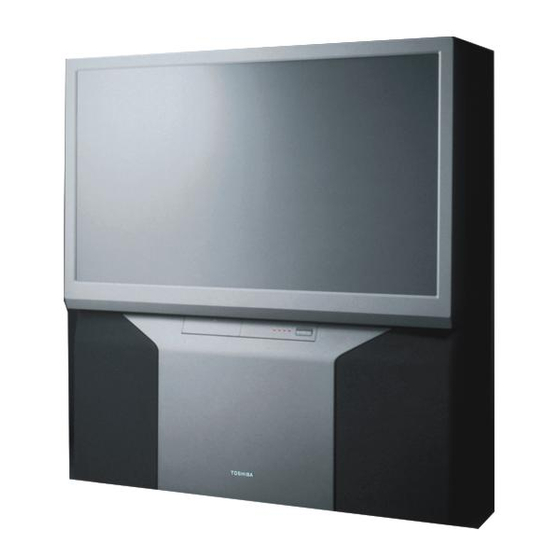
SPECIFICATIONS (Representative : 40PW03G) Rated voltage AC 230 V, 50/60 Hz Power consumption 150 W (at AC 220 V, 50 Hz) Dimensions × × 963.2 mm 1119.7 mm 466 mm (Width × Height × Depth) Mass 51.0 kg Screen size... - Page 71 TOSHIBA CORPORATION 1-1, SHIBAURA 1- CHOME, MINATO-KU, TOKYO 105-8001, JAPAN...
Need help?
Do you have a question about the 40PW03G and is the answer not in the manual?
Questions and answers