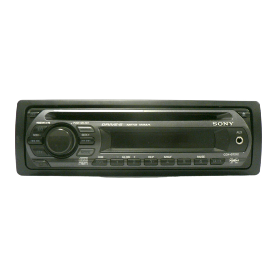
Sony CDX-GT210 Service Manual
Fm/mw/lw compact disc player
fm/mw/sw compact disc player
Hide thumbs
Also See for CDX-GT210:
- Operating instructions manual (32 pages) ,
- Installation/connections (2 pages) ,
- Service manual (40 pages)
Table of Contents
Advertisement
SERVICE MANUAL
Ver. 1.3 2007.03
• The tuner and CD sections have no adjustments.
CD player section
Signal-to-noise ratio
95 dB
Frequency response
10 – 20,000 Hz
Wow and flutter
Below measurable limit
Tuner section
FM
Tuning range
87.5 – 108 MHz
(CDX-GT210/GT212/GT262: EA)
87.5 – 108 MHz (at 50 kHz step)
(CDX-GT262: IND/GT262S)
87.5 – 107.9 MHz (at 200 kHz step)
(CDX-GT262: IND/GT262S)
FM tuning interval
50 kHz/200 kHz switchable
(CDX-GT262: IND/GT262S)
Antenna (aerial) terminal External antenna (aerial) connector
Intermediate frequency
10.7 MHz/450 kHz
Usable sensitivity
9 dBf
Selectivity
75 dB at 400 kHz
Signal-to-noise ratio
67 dB (stereo), 69 dB (mono)
Harmonic distortion at 1 kHz
0.5% (stereo), 0.3% (mono)
Separation
35 dB at 1 kHz
Frequency response
30 – 15,000 Hz
Sony Corporation
9-887-397-04
eVehicle Division
2007C04-1
Published by Sony Techno Create Corporation
© 2007.03
CDX-GT210/GT212/
Model Name Using Similar Mechanism CDX-GT111/GT161/GT161S
CD Drive Mechanism Type
Optical Pick-up Name
SPECIFICATIONS
MW/LW
Tuning range
MW tuning interval
Antenna (aerial) terminal External antenna (aerial) connector
Intermediate frequency
Sensitivity
SW (CDX-GT262/GT262S)
Tuning range
Antenna (aerial) terminal External antenna (aerial) connector
Intermediate frequency
Sensitivity
FM/MW/LW COMPACT DISC PLAYER
FM/MW/SW COMPACT DISC PLAYER
GT262/GT262S
AEP Model
UK Model
CDX-GT210/GT212
E Model
CDX-GT262/GT262S
Saudi Arabia Model
MG-101TA-188//Q
DAX-25A
MW: 531 – 1,602 kHz
(CDX-GT210/GT212/GT262: EA)
LW: 153 – 279 kHz (CDX-GT210/GT212: EA)
MW: 531 – 1,602 kHz (at 9 kHz step)
(CDX-GT262: IND/GT262S)
MW: 530 – 1,710 kHz (at 10 kHz step)
(CDX-GT262: IND/GT262S)
9 kHz/10 kHz switchable
(CDX-GT262: IND/GT262S)
10.7 MHz/450 kHz
MW: 30 µV, LW: 40 µV
SW1: 2,940 – 7,735 kHz
SW2: 9,500 – 18,135 kHz
(except for 10,140 – 11,575 kHz)
10.7 MHz/450 kHz
30 µV
– Continued on next page –
CDX-GT210/GT212
CDX-GT262/GT262S
CDX-GT262
Advertisement
Table of Contents


Need help?
Do you have a question about the CDX-GT210 and is the answer not in the manual?
Questions and answers