Table of Contents
Advertisement
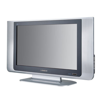
Service Manual
LCD TV
CHASSIS :
Model :
DLP-2612
DLP-3212
Caution
: In this Manual, some parts can be changed for improving. their
performance without notice in the parts list. So, if you need the
latest parts information, please refer to PPL(Parts Price List)in
Service Information Center.
S/M NO. : DSL210PEF0
SL-210P
NOV. 2005
Advertisement
Table of Contents

Related Manuals for Daewoo DLP-2612


Summary of Contents for Daewoo DLP-2612
-
Page 1: Service Manual
Service Manual LCD TV CHASSIS : SL-210P Model : DLP-2612 DLP-3212 Caution : In this Manual, some parts can be changed for improving. their performance without notice in the parts list. So, if you need the latest parts information, please refer to PPL(Parts Price List)in Service Information Center. -
Page 2: Table Of Contents
Contents 1. Safety Precaution 2. Product Specification 2-1. SPECIFICATION 2-2. Available Input Signal 3. BLOCK DIAGRAM 4. Description of Each BLOCK 4-1. Block Diagram of Main IC and TP 4-2. OVERVIEW 4-2-1. Y/C(S-Video) and SCART(CVBS,RGB) 4-2-2. RF CVBS 4-2-3. DTV/DVD Signal 4-2-4. -
Page 3: Safety Precaution
1. Safety Precautions (1) When moving or laying down a LCD Set, please deal with care. Avoid any impact towards the LCD Set. (2) Do not leave the broken LCD Set on for a long time. To prevent any further damages, after check the broken Set°Ø... -
Page 4: Product Specification
2. Product Specification 2-1. SPECIFICATION DLP-2612 DLP-3212 LCD Panel Screen Size 26” 32” Aspect Ratio 16:9 16:9 Resolution 1366 768 (WXGA) 1366 768 (WXGA) Pixel Pitch 0.4215mm 0.51075mm Contrast Ratio 800:1 800:1 TV System Receiving System PAL, SECAM PAL, SECAM... -
Page 5: Available Input Signal
2-2. Available Input Signal (1) PC/DVI/COMPONENT RESOLUTION V-freq D-SUB COMPONENT REMARK 640 480 IBM, VGA APPLE, MAC66 VESA VESA 720 400 IBM, VGA IBM, XGA2 800 600 VESA VESA VESA 832 624 MAC74 1024 768 VESA VESA 720P(1280 720) 1080i(1920 1080) 576P(704 576) 480P(720 480) 576i(704 576) -
Page 6: Block Diagram
3-1. MAIN BLOCK DIAGRAM... - Page 7 3-2. POWER BLOCK DIAGRAM...
-
Page 8: Block Diagram Of Main Ic And Tp
4-1. Block Diagram of main IC and TP ICU2 ICU3 TP564 TP565 ICJ10 TP566 ICS2 ICU10 TP603 ICL10 TP604 ICS3 ICS1 TP605 PW30 ICD10 TP159 TP160 JP11 TP161 TP246 ICA10 PW11 TP162 TP247 TP248 JP12 PW12 TP494 TP508 ICV10 TP495 TP509 TP496 TP529 PW15 JP206... - Page 9 -Flow Chart of RF, Video, S-Video Signal - Main Signal A. IC201 : Switching IC (Input: analog inputs, Output:: an analog output) B. ICV10 : Color Decoder (Input: Y/C, CVBS, R/G./B, Output: 8bit digital, H/V) C. ICS1 : Color Decoder/Image Processor(Input: 8bit Digital or 24bit Digital R/G/B, H/V,Output: 24bit Digital R/G/B, H/V) -Main TP (Input: Color Bar Pattern) ¡ÚCCV15(Y Signal), CCV14(C Signal), CCV16(CVBS Signal)
- Page 10 Color signal (input to ICV10) Location: LCV4 CVBS signal (Input to ICV10) Location: LCV1 Data Enable(Output of ICS1) Loacation(RCS15, ICD10.73PIN) -10-...
- Page 11 Horizontal sync (Out of ICS1) Location: RCS12, ICD10.72PIN Vertical sync (Out of ICS1) Location: RCS13, ICD10.71PIN Clock for display (Out of ICS1) Location: RCS14, ICD10.76PIN 4-2-2. TV signal Tuner(TU1) receives antenna signal and outputs CVBS and sound signal. For the main signal, IC201 switches out the CVBS and the rest of the signal flow is same as composite video signal flow mentioned earlier.
-
Page 12: Rf Cvbs
- Flow Chart of RF CVBS - Main Signal A. TU1 : Tuner (Input: antenna signal, Output: CVBS) B. IC201 : Switching IC (Input: CVBS, Output: CVBS) C. ICV10 : Vided processor (Input: CVBS, Output: 8bit Digital, H/V) D. ICS1 : Color Decoder/Image Processor(Input: 24bit Digital R/G/B, H/V, Output: 24bit Digital R/G/B, H/V) - Sub Signal(In PIP mode) A. - Page 13 - Flow Chart of COMPONENT - Main Signal A. ICI3 : Switching IC (Input: Component, Output: Component, H/V) B. ICA10 : A/D converter (Input: Component, H/V, Output: 24bit Digital RGB, H/V) C. ICS1 : Color Decoder/Image Processor(Input: 24bit Digital R/G/B, H/V,Output: 24bit Digital R/G/B, H/V) - Main TP (Input: 576I, Color Bar Pattern) Y signal (Input to ICA10)
- Page 14 Pr Signal (Input to ICA10) Location: LCA3, RCA11 Clock (Output of ICA10) Location: LCA1, RCA10 Horizontal sync (Output of ICA10) Location: RCA9 -14-...
-
Page 15: Pc Signal
Vertical sync (Output of ICA10) Location: RCA8 4-2-4. PC (Personal Computer) signal PC signal is switched out by ICI3 and input to ICA10 for A/D conversion. Then the signal goes through ICS1 for digital image processing. - Flow Chart of PC Signal - Main IC A. - Page 16 R Signal (Input to ICA10) Location: LCA3, RCA11 G Signal (Input to ICA10) Location: LCA4, RCA12 B Signal (Input to ICA10) Location: LCA5, RCA14 -16-...
-
Page 17: Dvi Signal
Clock (Output of ICA10) Location: LCA1, RCA10 Horizontal sync (Output of ICA10) Location: RCA9 Vertical sync (Output of ICA10) Location: RCA8 4-2-5 DVI (Digital Visual Interface) signal To process DVI signal, graphic card of AV device reads EDID data from ICI5(ROM). Then DVI signal is directly inputted to ICD10, which output digital 24bit RGB and H/V. - Page 18 - Flow Chart of DVI Signal - Main IC - Main IC A. ICI5 : ROM containing EDID data (EDID: display capabilities such as resolution, aspect A. ICI5 : ROM containing EDID data (EDID: display capabilities such as resolution, aspect ratio etc.) ratio etc.) B.
-
Page 19: Video Enhancer And Lvds Transmitter
Vertical sync (Output of ICD10) Location: RCD7 4-2-6. Video Enhancer and LVDS transmitter (for all inputs) Outputs of ICS1 are inputted to ICJ10(Video signal enhancer, MGDI) which improves picture quality greatly. Outputs of ICJ10 are inputted to ICL10 which is a LVDS transmitter. The converted LVDS signal is transmitted to the LCD panel. -
Page 20: Audio Signal Processing, Key And Led
R Signal (Input to ICV10) Location: LCV10, RCV30 G Signal (Input to ICV10) Location: LCV9, RCV28 B Signal (Input to ICV10) Location: LCV8, RCV26 4-2-8. Audio signal processing, KEY, and LED IC201 switches Audio signals and passes a switched signal to IC601 for audio signal processing. - Page 21 The outputs of IC601 are passed to IC604(right), and IC603(left) respectively to amplify the signals. KEY and LED PCBs send signals received from key buttons and LED to ICU10 for command processing. - Flow Chart of Audio Signal - Main IC A.
- Page 22 IC604, 605 INPUT Location: L out(CE605), R out(CE604) Tuner SIF Input Location: CC613, TU1.9PIN HEADPHONE Out Location: CE636, CE639 -22-...
-
Page 23: Power Pcb
Remote control signal Location: RCW17, CCW3 4-3. POWER PCB 4-3-1. POWER SPEC Rating: 220V~240V Regulating Method: Input Frequency: 50Hz Inrush Current: Below 80A at AC230V Output Voltage and Current are shown below Output Minimum output Maximum output Output Current Board Condition Voltage voltage... - Page 24 Ripple and Noise AC ripple, Switching Output voltage Output ripple and noise Condition Name Minimum output Maximum output Continuous voltage voltage +24V 22.8Vdc 25.2Vdc PWR-CTL +15V 14.25Vdc 15.75Vdc 500mVp-p 5.7Vdc 6.3Vdc Max Load 4.75Vdc 5.25Vdc ST+5V 4.75Vdc 5.25Vdc 500mVp-p PWR-CTL Other Lines Don’t Care 4-3-2.
- Page 25 C. PA11 Pin Spec (TEON-HO YMW025-08R 8p) PIN NO. OUT PUT ST +5V POWER ON : 3.3V PWR ON/OFF POWER ON : 4.5V AC DETECT POWER ON : 3.3V INV ON/OFF POWER ON : 0V A-DIMMING POWER ON 3.3V PWM-DIMMING D.
- Page 26 5-1. Checking initial menu data (1) Check initial data of User Menu 1) Picture - Mode : Standard - Brightness : 57 - Contrast : 80 - Color : 60 - Sharpness : 75 - Tint : 0 2) Sound - Mode : Standard - Balance : 0 - MPX : Mono...
-
Page 27: Service Mode
5-2. Entering SERVICE MODE There is two ways to enter Service Mode. First, you make use of the SERVICE REMOCON, you can enter Service Mode directly. Second, to enter SERVICE MODE with User Remocon, Adjust Sharpness ¡° 0¡±in Picture mode =>Adjust PR ¡° 99¡± => Press the ¡° Red¡± , ¡° Green¡±and ¡°... - Page 28 Function Name Details remark DEFAULT ADJUSTMENT OPERATING PC MODE PC SIGNAL ADJUSTMENT METHOO (IF EEPROM ERASE(S5) IS ON, THIS SETTING IS ERASED. DEFAULT ADJUSTMENT GAIN R PC ADJUSTMENT GAIN G GAIN B OFFSET R OFFSET G OFFSET B TELETEXT west-eu, east-eu, russia, greek, arabic, farci, arabich TTX language select OPTION OPTION...
- Page 29 To adjust WHITE BALANCE, refer to below process. A. To enter Service Mode, press button S1(when Service Remocon) or Adjust Sharpness ¡° 0¡±in Picture mode =>Adjust PR ¡° 99¡± => Press the ¡° Red¡± , ¡° Green¡±and ¡° Blue¡±Button => Press the ¡° menu¡±button.(when User Remocon) Then, HEAT RUN MODE IS CANCLED.
-
Page 30: Main & Sub Pcb Trouble Diagnosis
7-1. MAIN & SUB PCB Trouble Diagnosis 7-1-1. Common checking process when ¡° No signal¡±or ¡° No raster¡± No signal: OSD is working but no images are displaying No raster: OSD as well as images is not working Check Star t Is a w eak 1. - Page 31 CVBS signal (Positive polarity of CE220) B. When ¡° No Signal¡±in Y/C signal (S-Video) 1) First check if other inputs are working =>If other inputs are not working, replace MAIN or SUB PCB 2) Checking waveforms with Color Bar Pattern (Using the oscilloscope) - Main TP(Y signal): 7th pin of PW202(Top, Sub), Negative polarity of CE214(Top, Sub) near IC201, RC10(Bottom, Sub) near IC201, CCV15(Top, Main) near ICV10...
- Page 32 C. When ¡° No Signal¡±in Y/Pb/Pr signal (Component) 1) First check if other inputs are working =>If other inputs are not working, replace MAIN or SUB PCB 2) Checking waveforms with Color Bar Pattern (Using the oscilloscope) - Main TP (COMP1_Y): LCI27(Bottom, Main) near JP3, Second pin of ICI2, 4th pin of ICI2, 19th pin of ICI3, LCA4(Top, Main) near ICA10 - Main TP (COMP1_Pb): LCI22(Bottom, Main) near JP3, 5th pin of ICI2, 7th pin of ICI2, 14th pin of ICI3, LCA5(Top, Main) near ICA10...
-
Page 33: When No Signal Or No Raster
Pr Signal (LCA3) D. When ¡° No Signal¡±in PC 1) First check if other inputs are working =>If other inputs are not working, replace MAIN or SUB PCB 2) Checking waveforms with Color Bar Pattern (Using the oscilloscope) - Main TP (R signal): LCI3(Top, Main) near D-Sub Jack, 7th pin of ICI3, 21th pin of ICI3, LCA3(Top, Main) near ICA10 - Main TP (G signal): LCI4(Top, Main) near D-Sub Jack, 9th pin of ICI3, 19th pin of ICI3, LCA4(Top, Main) near ICA10... - Page 34 G Signal (LCA4) B Signal (LCA5) Clock (RCA10 near ICA10) -34-...
- Page 35 Horizontal sync (RCA9 near ICA10) Vertical sync (RCA8 near ICA10) E. When ¡° No Signal¡±in DVI 1) First check if other inputs are working =>If other inputs are not working, replace MAIN or SUB PCB 2) Checking waveforms with Color Bar Pattern (Using the oscilloscope) - Main TP (Clock): RCD5(Top, Main) near ICD10 - Main TP (H-Sync): RCD6(Top, Main) near ICD10 - Main TP (V-Sync): RCD7(Top, Main) near ICD10...
- Page 36 Horizontal sync (RCD6 near ICD10) Vertical sync (RCD7 near ICD10) -36-...
-
Page 37: When No Sound
7-1-2. When No Sound A. Overview Check Start 1. Check AC connection 2. Check Power S/W ON Do images display on screen? 3. Check Main or other PCBs Cancel Sound MUTE Check Sound Mute Off? Check the connection of Jack Is the Sound input Jack properly connected? (LCD and AV device) - Page 38 1) First check if images are displaying => If images are not displaying, replace MAIN or SUB PCB 2) Checking waveforms with 1Khz Sound pattern B. Main TP - Input to IC601: CE613(COMP2_L), CE614(COMP2_R), CE615(COMP1_L), CE616(COMP1_R), CE617(SUB_L), CE618(SUB_R), CE619(MAIN_L), CE620(MAIN_R), RC665(MONO), CC613(SIF) - Output to IC601: CE604(R OUT), CE605(L OUT) 1Khz Sound Signal (Input to IC 201) Location: PC-L(RC253, CE208), PC-R(RC254, CE209)
-
Page 39: When Control Key Does Not Operate
7-1-3. When Control Key does not operate Check S tart Check AC co nnect ion After turn on the powe r, Check Powe r S/ W ON does LED turn on red light? Check ot her PCBs Check the connection o f KEY PCB to MAIN PCB After ST-BY on Does LED turn on green ligh t? -
Page 40: When Remote Controller Does Not Operate
7-1-4. When Remote Controller does not operate. Check S tart Check AC co nnect ion After turn on the powe r, Check Powe r S/ W ON does LED turn on red light? Check other BLOCks Check the Battery of Remote Is Remote Controller working? Controller Check the connection between... -
Page 41: Power Pcb
7-2. POWER PCB Check Start 1. Check AC connection 2. Check Power S/W ON 3. Check F801(FUSE) After turn on the power, 4. Check C807 Voltage Does LED turn on light? 5. Check PA11.1 PIN (IT OPERATE 5V) 5. Check the Connector 1.Check the Connector 2. -
Page 42: Trouble Diagnosis
8-1. Facts you must know when trouble diagnosing or repairing. A. Trouble diagnosing and repairing of set mean find out which PCBs or blocks are not working and replace them with new PCBs. Repairing the broken PCBs are not necessary. Keep the broken PCBs and return them to service center or R&D center. B. -
Page 43: Typical Symptoms Of Pcb Problem Or Bad Connection
8-2. Typical Symptoms of PCBs problem or bad connection A. Symptom of initial latch up - Define initial latch up: When turn on the power, both LEDs light up red and TV is not working. - Repairing method: This is typical symptom when ROM(ICU3) is incorrectly connected at socket. - Page 44 HDTV 1.LCD MODULE 2. MAIN BOARD 3. SUB BOARD 4. POWER BOARD 5. FRONT MASK 6. BACK COVER 7. STAND 8. ALL CONNECTOR CONNECTION DAEWOO MGDi -44-...
- Page 45 COMPONENT PICTURE REMARK 1. LCD MODULE 2. MAIN BOARD 3. SUB BOARD 4. POWER BOARD -45-...
- Page 46 COMPONENT PICTURE REMARK 5. RONT MASK 6. BACK COVER 7. STAND 8. ALL CONNECTROR CONNECTION -46-...
-
Page 47: Dlp-2612Apsb Part List
10-1. DLP-2612APSB Part List PART CODE PART NAME DESCRIPTION REMARK PART CODE PART NAME DESCRIPTION REMARK ZZ100 48B5550K14 TRANSMITTER REMOCON R-50K14 (AA) 4850K01600 CORE FERRITE BNF-2629 ZZ110 PTACPWE125 ACCESSORY AS DLP-3212SPS ICU3U 149L04070Q IC CHIP FLASH MEMORY F49L040-70NP M821 4858213803 BAG INSTRUCTION L.D.P.E TO.05X250X400(+20) JP11... - Page 48 PART CODE PART NAME DESCRIPTION REMARK PART CODE PART NAME DESCRIPTION REMARK CCD8 HCBK104KBA C CHIP CERA 50V X7R 0.1MF K 1608 CCS1 HCQK200JBA C CHIP CERA 50V CH 20PF J 1608 CCD9 HCBK104KBA C CHIP CERA 50V X7R 0.1MF K 1608 CCS10 HCBK472KBA C CHIP CERA...
- Page 49 PART CODE PART NAME DESCRIPTION REMARK PART CODE PART NAME DESCRIPTION REMARK CCV32 HCBK152KBA C CHIP CERA 50V X7R 1500PF K 1608 RCI39 HRFT750JBA R CHIP 1/10 75 OHM J 1608 CCV33 HCQK151JBA C CHIP CERA 50V CH 150PF J 1608 RCI41 HRFT479JBA R CHIP...
- Page 50 PART CODE PART NAME DESCRIPTION REMARK PART CODE PART NAME DESCRIPTION REMARK RCS59 HRFT000-BA R CHIP 1/10 0 OHM 1608 CCA6 HCBK102KBA C CHIP CERA 50V X7R 1000PF K 1608 RCS7 HRFT472JBA R CHIP 1/10 4.7K OHM J 1608 CCA7 HCBK473KBA C CHIP CERA 50V X7R 0.047MF K 1608...
- Page 51 PART CODE PART NAME DESCRIPTION REMARK PART CODE PART NAME DESCRIPTION REMARK CEI34 HCELF220MD C CHIP ELECTRO 16V 22MF CM 4052 CES15 HCELF220MD C CHIP ELECTRO 16V 22MF CM 4052 CEI35 HCELH100MC C CHIP ELECTRO 25V 10MF CM 4052 CES16 HCELH221ME C CHIP ELECTRO 25V 220MF CM 8010...
- Page 52 PART CODE PART NAME DESCRIPTION REMARK PART CODE PART NAME DESCRIPTION REMARK ICL10 1DTC34LM85 IC CHIP TRANSMITTER DTC34LM85A LCP23 HFF600C00A F CHIP FERRITE BEAD 60 OHM UPB 2012 ICL11 TFDS4953-C FET CHIP FDS4953 SO-8 -30V -5A REEL LCP24 HLC100J00A L CHIP COIL 10UH NLC322522 ICP1 1A1117E33D...
- Page 53 PART CODE PART NAME DESCRIPTION REMARK PART CODE PART NAME DESCRIPTION REMARK RAJ14 HRTS8E330J R CHIP ARRAY 1/16 8P 33 OHM J 3216 RCL10 HRFT000-BA R CHIP 1/10 0 OHM 1608 RAJ15 HRTS8E330J R CHIP ARRAY 1/16 8P 33 OHM J 3216 RCL11 HRFT201JBA R CHIP...
- Page 54 PART CODE PART NAME DESCRIPTION REMARK PART CODE PART NAME DESCRIPTION REMARK RCV7 HRFT103JBA R CHIP 1/10 10K OHM J 1608 CC201 HCBK102KBA C CHIP CERA 50V X7R 1000PF K 1608 RCV9 HRFT000-BA R CHIP 1/10 0 OHM 1608 CC202 HCBK102KBA C CHIP CERA 50V X7R 1000PF K 1608...
- Page 55 PART CODE PART NAME DESCRIPTION REMARK PART CODE PART NAME DESCRIPTION REMARK CC649 HCBK103KBA C CHIP CERA 50V X7R 0.01MF K 1608 RC244 HRFT101JBA R CHIP 1/10 100 OHM J 1608 CC651 HCBK104KBA C CHIP CERA 50V X7R 0.1MF K 1608 RC246 HRFT101JBA R CHIP...
- Page 56 PART CODE PART NAME DESCRIPTION REMARK PART CODE PART NAME DESCRIPTION REMARK RC630 HRFT102JBA R CHIP 1/10 1K OHM J 1608 CE616 HCEJK109MC C CHIP ELECTRO MV 50V 1MF 4.0DX5.3H RC631 HRFT123JBA R CHIP 1/10 12K OHM J 1608 CE617 HCEJK109MC C CHIP ELECTRO MV 50V 1MF 4.0DX5.3H...
- Page 57 PART CODE PART NAME DESCRIPTION REMARK HRFT000-BA R CHIP 1/10 0 OHM 1608 LC200 HLC100J00A L CHIP COIL 10UH NLC322522 LC201 HFEACF470B F CHIP EMI ACF321825 47P LC202 HFEACF470B F CHIP EMI ACF321825 47P LC203 HFEACF470B F CHIP EMI ACF321825 47P LC204 HFEACF470B F CHIP EMI...
-
Page 58: Dlp-3212Apsb Difference Part List
10-2. DLP-3212APSB Difference Part List PART CODE PART NAME PART DESCRIPTION DLP-2612APSB DLP-3212APSB 4852090911 M201 MASK FRONT ABS GY PTFMSJE134 4852090811 M201 MASK FRONT ABS GY PTFMSJE125 4857743800 M201A CUSION PANEL PVC 400 X 10 T=1.0 PTFMSJE134 PTFMSJE125 4852173011 M211 COVER BACK ABS GY PTBCSHE134... - Page 59 PART CODE PART NAME PART DESCRIPTION DLP-2612APSB DLP-3212APSB PTSBJRG098 ZZ200 PCB SUB RADIAL AS DLP-2612APSB PTSBJBG098 PTSBJAG098 ZZ200 PCB SUB AXIAL AS DLP-2612APSB PTSBJRG098 PTSBJ2G098 ZZ200 PCB SUB CHIP B AS DLP-2612APSB PTSBMSG098 PTMPJ0G099 ZZ200 PCB MAIN (RHU) AS DLP-3212APSB PTMPJ2G099 PTMPJ1G099 ZZ200...
- Page 60 11. SCHEMATIC DIAGRAM...
-
Page 61: Schematic Diagram
SCHEMATIC DIAGRAM... - Page 62 SCHEMATIC DIAGRAM...
- Page 63 SCHEMATIC DIAGRAM...
- Page 64 SCHEMATIC DIAGRAM...
- Page 65 SCHEMATIC DIAGRAM...
- Page 66 SCHEMATIC DIAGRAM...
- Page 67 SCHEMATIC DIAGRAM...
- Page 68 SCHEMATIC DIAGRAM...
- Page 69 SCHEMATIC DIAGRAM...
- Page 70 SCHEMATIC DIAGRAM...
- Page 71 SCHEMATIC DIAGRAM...
- Page 72 SCHEMATIC DIAGRAM...
- Page 73 SCHEMATIC DIAGRAM...
- Page 74 SCHEMATIC DIAGRAM...
- Page 75 10.1 DLP-3212APSB...
- Page 76 10.2 DLP-2612APSB...
- Page 77 DAEWOO ELECTRONICS CORP. 686, AHYEON-DONG, MAPO-GU, SEOUL, KOREA. C.P.O. BOX 8003 SEOUL KOREA PRINTED DATE : NOV. 2005...
Need help?
Do you have a question about the DLP-2612 and is the answer not in the manual?
Questions and answers