Table of Contents
Advertisement
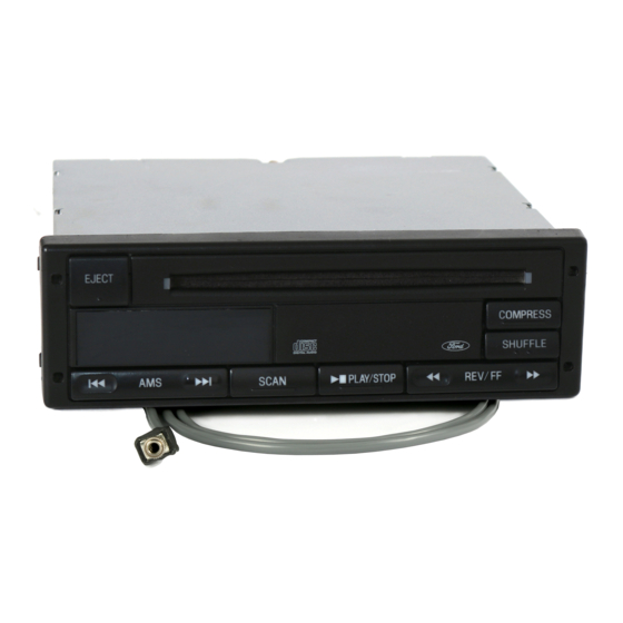
SERVICE MANUAL
The electrical adjustments are done
automatically in this set.
System
Compact disc digital audio system
Disc
Compact disc
Laser
Semiconductor laser (λ=780 nm)
Spindle speed
200 r.p.m. to 500 r.p.m. (CLV)
Error correction
Sony Super Strategy Cross Interleave Read
Solomon Code
Number of channels
2
D-A conversion
1-bit
Frequency response
20 to 20,000 Hz
Harmonic distortion
0.02% (1 kHz)
Dynamic range
85 dB
Signal to noise ratio
85 dB
Channel separation
70 dB
Wow and flutter
Below measurable limit
Outputs
Ford Signal Connector
MICROFILM
XR3F-19B160
SPECIFICATIONS
+1.0
dB
–1.5
Model Name Using Similar Mechanism
CD Drive Mechanism Type
Optical Pick-Up Name
Disc
Track pitch
1.6 µm
Sampling frequency
44.1 kHz
Quantization
16 bit linear quantizing/channel
Modulation system
EFM
Transfer rate
2.03 Mbit/sec. (before modulation)
General
Power requirements
14.4 V dc car battery (negative ground)
Current drain
1 A (playback)
2 A (during disc loading or eject)
Operating temperature
–20˚C to +60˚C (–4˚F to +120˚F)
Approx. 188 × 59 × 160.6 mm (w/h/d)
Dimensions
(7-1/2 × 2-7/20 × 6-2/5 in.)
including projecting parts and controls
Weight
Approx. 1.3 kg (3 lb), net
COMPACT DISC PLAYER
US Model
Version: –AA
F8ZF-19B160
MG-205F-132
KSS-313B/Z-N
Advertisement
Table of Contents

Related Manuals for Sony XR3F-19B160


Summary of Contents for Sony XR3F-19B160
- Page 1 Sampling frequency 44.1 kHz Quantization 16 bit linear quantizing/channel Spindle speed 200 r.p.m. to 500 r.p.m. (CLV) Error correction Sony Super Strategy Cross Interleave Read Modulation system Solomon Code Transfer rate 2.03 Mbit/sec. (before modulation) Number of channels General D-A conversion 1-bit +1.0...
-
Page 2: Table Of Contents
LINE WITH MARK ! ON THE SCHEMATIC DIAGRAMS AND IN THE PARTS LIST ARE CRITICAL TO SAFE OPERATION. REPLACE THESE COMPONENTS WITH SONY PARTS WHOSE PART NUMBERS APPEAR AS SHOWN IN THIS MANUAL OR IN SUPPLEMENTS PUB- LISHED BY SONY. -
Page 3: Disassembly
SECTION 1 DISASSEMBLY Note: Follow the disassembly procedure in the numerical order given. CASE 1 screw (PTT2.6 × 5) case 1 screw (K2.6 × 6) FRONT PANEL 6 flat cable (CN104) 2 screw (K2.6 × 6) 3 reinforcement front panel 3 reinforcement 4 two claws 2 screw (K2.6 ×... -
Page 4: Ic Block Diagrams
SECTION 2 DIAGRAMS • IC Block Diagrams IC301 PCM1710U-A/1K (MD MAIN BOARD) IC302 SM5852CS-E2 (MD MAIN BOARD) LRCI DB/DS INPUT LRCIN ML/DSD BCKI MOD2 INTERFACE DIGITAL MOD1 SIGNAL INPUT PROCESSOR MC/DM2 INTERFACE DIGITAL MODE SYSTEM FILTER CONTROL CLOCK BCKIN MD/DM1 LRCO SEQUENTIAL TIMING... - Page 5 IC501 CXA1782BR (MD MAIN BOARD) IC502 CXD2507AQ (MD MAIN BOARD) IC101 BA3129F-T1 (MAIN BOARD) +IN1A +IN2A 27 26 25 –IN2A –IN1A +IN1B +IN2B SERVO AUTO DATA SEQUENCER –IN2B XRST –IN1B SENS SUB CODE MUTE OUT1 OUT2 INTERFACE PROCESSOR DIGITAL LOCK SQCK TEST SQSO...
-
Page 6: Block Diagram -Servo Section
XR3F-19B160 2-1. BLOCK DIAGRAM – SERVO Section – DIGITAL SIGNAL PROCESSOR, FILTER CLV SERVO IC502 C16M CLOCK XTAI RF AMP GENERATOR PHD1 (Page 7) DETECTOR ASYMMETRY PCMD DATA SUMMING DIGITAL PLL DOUT RF AMP CORRECTION DEMODULATOR BCKI BCKO PHD2 (Page 7) -
Page 7: Block Diagram -Main Section
XR3F-19B160 2-2. BLOCK DIAGRAM – MAIN Section – • SIGNAL PATH AUDIO IN R-CH : CD PLAY AUDIO IN L-CH LINE AMP & SWITCH IC101 +5V DRIVER, +5V ACC BACK-UP REGULATOR Q401 DIGITAL FILTER, SERVO B+ SWITCH D/A CONVERTER IN2A... -
Page 8: Note For Printed Wiring Boards And Schematic Diagrams
• Circuit Boards Location • Waveforms (MD MAIN BOARD) 1 IC501 $™ (TEO) 5 IC502 @™ (BCK) POWER CONNECTOR board Approx. 5 Vp-p SIGNAL CONNECTOR board 156 mVp-p SENSOR board MAIN board 470 ns 2 IC501 1 (FEO) 6 IC601 ^ª (X2) Approx. -
Page 9: Printed Wiring Boards -Servo Section
XR3F-19B160 2-4. PRINTED WIRING BOARDS – SERVO Section – (Page 12) • Semiconductor Location Ref. No. Location Ref. No. Location Ref. No. Location D801 A-11 IC502 G-10 Q504 D802 IC601 Q505 D804 IC602 Q602 Q603 IC301 F-11 Q301 Q604 IC302... -
Page 10: Schematic Diagram -Servo Section (1/2)
XR3F-19B160 2-5. SCHEMATIC DIAGRAM – SERVO Section (1/2) – • See page 8 for Waveforms. • See page 4 for IC Block Diagrams. The components identified by mark ! or dotted line with mark ! are critical for safety. Replace only with part number specified. -
Page 11: Schematic Diagram -Servo Section (2/2)
XR3F-19B160 2-6. SCHEMATIC DIAGRAM – SERVO Section (2/2) – • See page 8 for Waveforms. • See page 4 for IC Block Diagrams. (Page 13) -
Page 12: Printed Wiring Boards -Main Section
XR3F-19B160 2-7. PRINTED WIRING BOARDS – MAIN Section – • See page 8 for Circuit Boards Location. (Page 9) • Semiconductor Location Ref. No. Location Ref. No. Location D302 Q101 D303 Q201 D401 Q301 Q302 D402 D403 Q304 D404 Q401... -
Page 13: Schematic Diagram -Main Section
XR3F-19B160 2-8. SCHEMATIC DIAGRAM – MAIN Section – • See page 5 for IC Block Diagrams. (Page (Page... -
Page 14: Printed Wiring Board -Key Board
XR3F-19B160 2-9. PRINTED WIRING BOARD – KEY Board – • See page 8 for Circuit Boards Location. 2-10. SCHEMATIC DIAGRAM – KEY Board – • See page 5 for IC Block Diagram. (Page 12) (Page... -
Page 15: 2-11. Ic Pin Function Description
2-11. IC PIN FUNCTION DESCRIPTION • MD MAIN BOARD IC601 µPD78052GC-123-3B9 (SYSTEM CONTROLLER) Pin No. Pin Name Description Disc size (8 cm/12 cm) detect signal input from the photosensor (Q604) PH1IN “L”: 8 cm, “H”: 12 cm PH2OR3 Disc in detect signal input from the photosensor (Q605) “H”: disc is present Disc loading completion detect signal input from the photosensor (Q607) PH4IN... - Page 16 Pin No. Pin Name Description Focusing gain automatic alignment signal output to the focus coil driver (IC402) — — Not used (open) Reset signal output to the SM5852CS (IC302), CXA1782BR (IC501) and CXD2507AQ (IC502) XRST “L”: reset DCLK Serial data transfer clock signal output to the CXD2507AQ (IC502) DDATA Serial data output to the CXD2507AQ (IC502) DLAT...
-
Page 17: Exploded Views
SECTION 3 EXPLODED VIEWS NOTE: • -XX and -X mean standardized parts, so they • Items marked “*” are not stocked since they The components identified by mark ! or dotted line with mark are seldom required for routine service. Some may have some difference from the original ! are critical for safety. - Page 18 (2) KEY BOARD UNIT PL504-507 VFD501 PL501-503 Ref. No. Part No. Description Remark Ref. No. Part No. Description Remark * 51 A-3291-761-A PANEL ASSY 3-913-335-02 SPACER 3-913-332-11 BUTTON, SEESAW (= AMS +) 3-913-328-02 COVER, DISPLAY 3-913-333-11 BUTTON (SCAN) 3-917-138-01 SPACER 3-913-333-01 BUTTON ((p PLAY/STOP) * 71 3-917-809-01 SHEET, INSULATING...
- Page 19 (3) MECHANISM DECK SECTION-1 (MG-205F-132) M903 Ref. No. Part No. Description Remark Ref. No. Part No. Description Remark * 101 A-3309-934-A MD MAIN BOARD, COMPLETE 3-384-908-31 ARM, CHUCKING 3-384-894-01 GEAR (R1 3-384-888-01 SLIDER (L) 3-384-900-01 SPRING (PRESS) 3-384-887-01 LEVER (L) 3-578-242-11 WASHER * 126 3-906-923-03 GUIDE (DISK 2)
- Page 20 (4) MECHANISM DECK SECTION-2 (MG-205F-132) M901 M902 Ref. No. Part No. Description Remark Ref. No. Part No. Description Remark A-3252-586-A SHAFT (SL) ASSY 3-384-912-11 GEAR (K2) ! 152 8-848-407-11 OPTICAL PICK-UP (KSS-313B/Z-RP) 3-570-615-02 POLY-WASHER (DIA.1.2) 3-384-922-01 GEAR (SL FEED) 3-384-913-11 SPRING (THRUST RETAINER) 3-384-920-11 RETAINER (SL FEED) 3-918-103-11 SCREW (TOOTH) (+P 2) * 155...
-
Page 21: Electrical Parts List
SECTION 4 MAIN ELECTRICAL PARTS LIST NOTE: • Due to standardization, replacements in the • Items marked “*” are not stocked since they The components identified by mark ! or dotted line with mark parts list may be different from the parts speci- are seldom required for routine service. - Page 22 MAIN Ref. No. Part No. Description Remark Ref. No. Part No. Description Remark C111 1-163-124-00 CERAMIC CHIP 200PF D404 8-719-110-21 DIODE RD11ES-B1 C112 1-135-149-21 TANTALUM CHIP 2.2uF D405 8-719-938-78 DIODE SB10-05PCP C113 1-163-138-00 CERAMIC CHIP 750PF D406 8-719-109-88 DIODE RD5.6ES-B1 D408 8-719-109-86 DIODE RD5.1ES-B3 C201...
- Page 23 MAIN MD MAIN Ref. No. Part No. Description Remark Ref. No. Part No. Description Remark R214 1-216-073-00 METAL CHIP 1/10W C302 1-107-826-11 CERAMIC CHIP 0.1uF R215 1-216-097-00 RES, CHIP 100K 1/10W C303 1-135-166-21 TANTALUM CHIP 47uF R301 1-216-121-00 RES, CHIP 1/10W C304 1-109-982-11 CERAMIC CHIP...
- Page 24 MD MAIN Ref. No. Part No. Description Remark Ref. No. Part No. Description Remark C619 1-164-004-11 CERAMIC CHIP 0.1uF R506 1-216-001-00 METAL CHIP 1/10W R507 1-216-832-11 METAL CHIP 8.2K 1/16W < CONNECTOR > R509 1-216-833-11 RES, CHIP 1/16W CN601 1-750-992-21 CONNECTOR, FPC 25P R510 1-216-845-11 METAL CHIP 100K...
- Page 25 MD MAIN MOTOR POWER CONNECTOR SENSOR SIGNAL CONNECTOR Ref. No. Part No. Description Remark Ref. No. Part No. Description Remark R630 1-216-825-11 METAL CHIP 2.2K 1/16W 1-654-932-11 SIGNAL CONNECTOR BOARD R631 1-216-825-11 METAL CHIP 2.2K 1/16W ************************ R640 1-216-821-11 METAL CHIP 1/16W R641 1-216-829-11 METAL CHIP...
- Page 26 XR3F-19B160 Sony Corporation 9-926-580-11 99F05019-1 Mobile Electronics Company Printed in Japan © 1999. 6 Published by Quality Assurance Dept.
Need help?
Do you have a question about the XR3F-19B160 and is the answer not in the manual?
Questions and answers