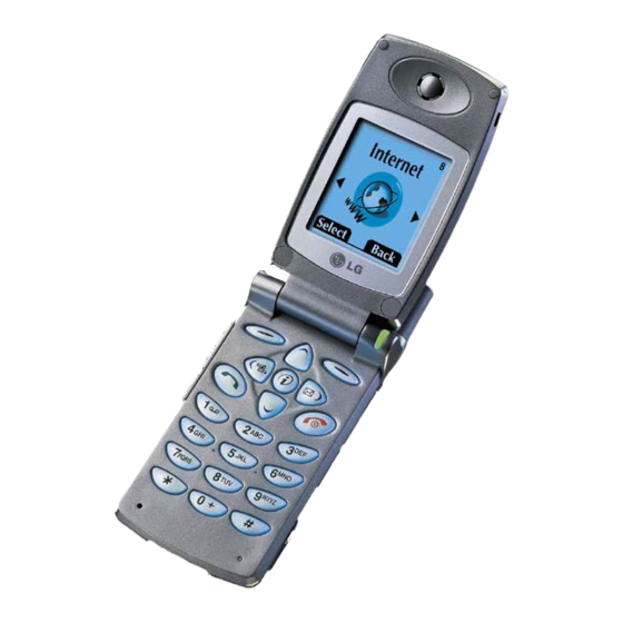
LG -510W Service Manual
Hide thumbs
Also See for LG-510W:
- Service manual (47 pages) ,
- User manual (202 pages) ,
- User manual (99 pages)
Table of Contents
Advertisement
Quick Links
Download this manual
See also:
User Manual
Advertisement
Table of Contents

Related Manuals for LG LG-510W


Summary of Contents for LG LG-510W
- Page 1 GSM Phone SERVICE MANUAL MODEL : LG - 510W...
-
Page 2: Table Of Contents
Table Of Contents 6. STAND ALONE TEST ......1. Introduction ..........6.1 Introduction ..........74 1.1 Purpose ........... 2 6.2 Setting Method ........74 1.2 Regulatory Information ......2 6.3 Means of Test ........74 1.3 Abbreviations ........... 4 7. AUTO CALIBRATION ...... -
Page 3: Introduction
A local telephone company may make changes in its communications facilities or procedure. If these changes could reasonably be expected to affect the use of the LG-510W or compatibility with the network, the telephone company is required to give advanced written notice to the user, allowing the user to take appropriate steps to maintain telephone service. - Page 4 1. Introduction E. Notice of Radiated Emissions The LG-510W complies with rules regarding radiation and radio frequency emission as defined by local regulatory agencies. In accordance with these agencies, you may be required to provide information such as the following to the end user.
-
Page 5: Abbreviations
Global System for Mobile Communications IPUI International Portable User Identity Intermediate Frequency Liquid Crystal Display Low Drop Output Light Emitting Diode LG-510W LG GSM Phone LG Electronics OPLL Offset Phase Locked Loop Power Amplifier Module Printed Circuit Board Programmable Gain Amplifier Phase Locked Loop... - Page 6 1. Introduction Travel Adapter Time Division Duplex TDMA Time Division Multiple Access UART Universal Asynchronous Receiver/Transmitter Voltage Controlled Oscillator VCTCXO Voltage Control Temperature Compensated Crystal Oscillator Wireless Application Protocol - 5 -...
-
Page 7: Performance
2. PERFORMANCE 2. PERFORMANCE 2.1 H/W Features Item Feature Li-Polymer, 630 mAh Standard Battery Size: 44 68.6 5.6 mm Weight: 22 g Li-Ion, 940 mAh Extended Battery Size: 44 68.6 8.7 mm Weight: 32 g AVG TCVR Current GSM , EGSM: 243 mA, DCS: 209 mA Stand by Current <... -
Page 8: Technical Specification
2. PERFORMANCE 2.2 Technical Specification Item Description Specification TX: 890 + n 0.2 MHz RX: 935 + n 0.2 MHz (n = 1 ~ 124) EGSM Frequency Band TX: 890 + (n – 1024) 0.2 MHz RX: 935 + (n – 1024) 0.2 MHz (n = 975 ~ 1024) TX: 1710 + (n –... - Page 9 2. PERFORMANCE Item Description Specification GSM, EGSM Offset from Carrier (kHz). Max. dBc +0.5 600 ~ 1,200 1,200 ~ 1,800 1,800 ~ 3,000 3,000 ~ 6,000 Output RF Spectrum 6,000 (due to modulation) Offset from Carrier (kHz). Max. dBc +0.5 600 ~ 1,200 1,200 ~ 1,800 1,800 ~ 3,000...
- Page 10 2. PERFORMANCE Item Description Specification GSM, EGSM BER (Class II) < 2.439% @-102 dBm Bit Error Ratio BER (Class II) < 2.439% @-100 dBm RX Level Report Accuracy 3 dB 8 3 dB Frequency (Hz) Max.(dB) Min.(dB) Sending Response 1,000 2,000 3,000 3,400...
- Page 11 2. PERFORMANCE Item Description Specification ≤ 30 ppm 32.768KHz tolerance Full power < 243 mA (GSM, EGSM) ; < 209 mA (DCS) Power Consumption Standby - Normal ≤ 3 mA (Max. power) - Using Test mode on DSP Sleep function ≤ 6 mA GSM/ Level 7 (Battery Capacity 630mA): 162 Min Talk Time GSM/ Level 12 (Battery Capacity 630mA): 240 Min...
-
Page 12: Technical Brief
3. TECHNICAL BRIEF 3. TECHNICAL BRIEF 3.1 Receiver The receiver part contains all active circuits for a complete, full receiver chain with the exception of RF PLL VCO(U302) and discrete RF SAW filters. The filtered and amplified signal is processed from the RF-mixer inputs to the baseband(BB) output. - Page 13 3. TECHNICAL BRIEF A. RF front end The RF receive signals(GSM 925MHz ~ 960MHz, DCS 1805MHz ~ 1880MHz) are input via the antenna or coaxial connector. An antenna matching circuit is between the antenna and the connector. The FEM(FL301) is used to control the Rx and TX paths. And, the input signals VC1 and VC2 of a FL301 are connected to 2-Input AND Gates(U306,U307) to switch either TX or RX path on.
- Page 14 3. TECHNICAL BRIEF C. RX I/Q Demodulator The amplified IF signal at 45 MHz passes to the demodulator and is mixed down to DC to generate I and Q BB signals. The BB signals pass via integrated low-pass filters to the BB A/D converters. The remainder of the channel filtering is performed by the BB chipset.
-
Page 15: Synthesizer
3. TECHNICAL BRIEF 3.2 Synthesizer The synthesizer IC, the Si4133G-XM2, comprises three complete PLLs. One, which is active all of the time and in this application produces a constant 1080MHz. This is the IF oscillator and is divided down inside the HD 155128 to produce the 270 MHz for the second receive mixer, and with an optional further division to 135 MHz for the transmitter quadrature modulator. - Page 16 3. TECHNICAL BRIEF Table 3-6. Si4133G-XM2 VCO Characteristics. Fcen Range (MHz) Lext Range ( nH ) Cnom ( pF ) Lpkg ( nH ) 1720 1429 1080 Figure 3-3. Synthesizer Internal Block Diagram. - 15 -...
- Page 17 3. TECHNICAL BRIEF The IF and RF output frequencies are set by programming the N Divider registers. All three PLL R Dividers are fixed at R = 65 to yield a 200 kHz phase detector update rate from a 13 MHz reference frequency.
-
Page 18: Transmitter
3. TECHNICAL BRIEF 3.3 Transmitter The Transmitter part contains HD155128TF active parts and PAM, APC IC, coupler, FEM(front-end module) circuit. The HD155128TF active part consists of a vector modulator and offset phase- locked loop block(OPLL) including down-converter, phase detector, loop filter and dual band transmit VCO which can operate at either final RF output frequency. - Page 19 3. TECHNICAL BRIEF A. TX IF Modulator The TX I and Q signals from BB analog chipset, AD6521(U2), #F9, E9, C9, D9 are fed to #17~20 of the HD155128TF TX modulator(U301), where they are then modulated onto either a TX IF of 270MHz(for GSM-TX) or 135MHz(for DCS-TX) by the quadrature mixer inside U301.
- Page 20 3. TECHNICAL BRIEF B. OPLL The down converter contained inside of the HD155128TF (U301) mixes the TX RF frequency with the RF VCO signal from the Si4133G-XM2 (U302) to generate a `feedback' signal at 270 MHz for GSM and EGSM operation or 135 MHz for DCS operation. The `feedback' signal passes via a limiter to one port of the phase detector.
- Page 21 3. TECHNICAL BRIEF Figure 3-7. Power Amplifier and its Control Part Circuits. D. PA Circuit and Control The power amplifier control circuit ensures that the RF signal is regulated to the required limits of operation. RF power is controlled by driving the power control pins of power amplifier and sensing the resultant RF output power via a directional coupler (U305).
-
Page 22: 13Mhz Clock
3. TECHNICAL BRIEF 3.4 13MHz Clock The 13 MHz clock (VC-TCXO-208C) consists of a TCXO (Temperature Compensated Crystal Oscillator) which oscillates at a frequency of 13 MHz. It is used within the Si4133G_XM2 Synthesizers, BB Analog chip-set (AD6521), and Digital (AD6522). -
Page 23: Digital Main Processor
3. TECHNICAL BRIEF 3.6 Digital Main Processor Figure 3-10. System Interconnection of the AD6522 External Interfaces - 22 -... - Page 24 3. TECHNICAL BRIEF Interconnection with external devices A. RTC block interface Countered by external X-TAL The X-TAL oscillates 32.768KHz B. LCD module interface Controlled by LCD_CS, LCD_RES, LCD_A0, /WR, /RD, DATA [00...07] ports Table 3-8. LCD Module Interface. Description LCD_CS LCD chip enable LCD_RES This pin resets LCD module...
- Page 25 The AD6522 check status periodically in call mode if SIM card is inserted or not , but the AD6522 don't check in deep sleep mode. Interface by SIM_IO, SIM_CLK, SIM_RST Table 3-10. SIM Interface. Description This pin receives and sends data to SIM card. LG-510W support only 3.0 volt SIM_IO interface SIM card. SIM_CLK Clock 3.5MHz frequency...
-
Page 26: Analog Main Processor
AFC DAC: 13 bits IDAC: 10 bits D. Voiceband section Receive audio signal from MIC. LG-510W use differential configuration. Send audio signal to Speaker. LG-510W use differential configuration. It interconnect with external device like main microphone, main speaker, ear-phone and Hands free kit through the VINNORP, VINNORN, VOUTNORP, VOUTNORN, VINAUXP, VINAUXN, VOUTAUXP, VOUTAUXN and BUZZER port. -
Page 27: Power Management
3. TECHNICAL BRIEF 3.8 Power Management ADP3408 Figure 3-12. ADP3408 Inner Block Diagram. - 26 -... - Page 28 2.80 V (is provided to Flash) D. Battery charging block It can be used to charge Lithium Ion and/or Nickel Metal Hydride batteries. LG-510W use Li-Ion and Li-polymer battery only. Charger initialization, trickle charging, and Li-Ion charging control are implemented in hardware.
-
Page 29: Memories
Extended battery (Optional): Capacity - 940 mAh, Li-Ion 3.9 Memories 32M flash memory + 4M SRAM 16 bit parallel data bus ADD01 ~ ADD21 RF Calibration data art stored in Flash (LG-510W do not use EEPROM) 3.10 Display and Interface Table 3-12. LCD Module. Description Display format... - Page 30 3. TECHNICAL BRIEF Figure 3-13. Keypad Switches and Scanning. - 29 -...
-
Page 31: Microphone
3. TECHNICAL BRIEF 3.12 Microphone The microphone is soldered to the main PCB. The audio signal is passed to VINNORP (#K8) and VINNORN (#K7) pins of the AD6522. The voltage supply 2V45_VAN is output from the ADP3408, and is a bias voltage for both the VINNOR (through R41) and VINAUX (through R54) lines. The VINNOR or VINAUX signal is then A/D converted by the Voiceband ADC part of the AD6521. -
Page 32: Hands-Free Interface
3. TECHNICAL BRIEF 3.14 Hands-free Interface The audio out (VOUTAUXP and VOUTAUXN) to the hands-free kit consists of a pair of differential signals from the AD6521 auxiliary outputs (#K9, #K6), which are tracked down the board to carkit connector (CN3) at the base of the handset. The DC level of the signal is supplied to the VOUTAUX pin. -
Page 33: Key Back-Light Illumination
3. TECHNICAL BRIEF 3.16 Key Back-light Illumination In key back-light illumination, there are 8 green LEDs in Main Board, which are driven by KEY_BACKLIGHT line from the AD6522. Figure 3-17. Key Back-light Illumination. 3.17 LCD Back-light Illumination In LCD back-light illumination, there is an EL driver in FPCB Board and EL sheet in LCD Module, which is driven by LCD_BACKLIGHT line from the AD6522. -
Page 34: Trouble Shooting
4. TROUBLE SHOOTING 4. TROUBLE SHOOTING Fig. 4-1 shows a measurement set-up. Figure 4-1. Measurement Set-up - 33 -... -
Page 35: Rx Trouble
4. TROUBLE SHOOTING 4.1 RX Trouble - 34 -... - Page 36 4. TROUBLE SHOOTING • RX Level Check (EGSM) - 35 -...
- Page 37 4. TROUBLE SHOOTING • RX Level Check (DCS) - 36 -...
-
Page 38: Tx Trouble
4. TROUBLE SHOOTING 4.2 TX Trouble - 37 -... - Page 39 4. TROUBLE SHOOTING • TX Level Check - 38 -...
- Page 40 4. TROUBLE SHOOTING • Replacement of a PAM A PAM (Power Amplifier Module ; U303) may need to be replaced with new one due to following problems. - Can not make a call after serious damage / impact on the phone or dropping the phone. - Can not make a call again after sending or receiving call.
-
Page 41: Power On Trouble
4. TROUBLE SHOOTING 4.3 Power on Trouble - 40 -... - Page 42 4. TROUBLE SHOOTING - 41 -...
-
Page 43: Charge Trouble
4. TROUBLE SHOOTING 4.4 Charge Trouble - 42 -... -
Page 44: Lcd Trouble
4. TROUBLE SHOOTING 4.5 LCD Trouble - 43 -... -
Page 45: Receiver Trouble
4. TROUBLE SHOOTING 4.6 Receiver Trouble - 44 -... -
Page 46: Buzzer Trouble
4. TROUBLE SHOOTING 4.7 Buzzer Trouble - 45 -... -
Page 47: Mic Trouble
4. TROUBLE SHOOTING 4.8 MIC Trouble ± ± - 46 -... -
Page 48: Vibrator Trouble
4. TROUBLE SHOOTING 4.9 Vibrator Trouble - 47 -... -
Page 49: Indicator Led Trouble
4. TROUBLE SHOOTING 4.10 Indicator LED Trouble - 48 -... - Page 50 4. TROUBLE SHOOTING - 49 -...
-
Page 51: Backlight Led Trouble
4. TROUBLE SHOOTING 4.11 Backlight LED Trouble - 50 -... -
Page 52: Folder On/Off Trouble
4. TROUBLE SHOOTING 4.12 Folder on/off Trouble - 51 -... -
Page 53: Sim Detect Trouble
4. TROUBLE SHOOTING 4.13 SIM Detect Trouble - 52 -... -
Page 54: Earphone Trouble
4. TROUBLE SHOOTING 4.14 Earphone Trouble - 53 -... - Page 55 4. TROUBLE SHOOTING - 54 -...
-
Page 56: Hfk Trouble
4. TROUBLE SHOOTING 4.15 HFK Trouble - 55 -... - Page 57 4. TROUBLE SHOOTING - 56 -...
-
Page 58: Test Point Data
5. TEST POINT DATA 5. TEST POINT DATA A. Received RF Level and Checks This section shows the typical RF levels expected throughout the receiver path. A block diagram showing the locations of the RF measurement points and levels is shown in Fig. 5-4. •... - Page 59 5. TEST POINT DATA B. Transmitted RF Level and Checks This section shows the typical RF levels expected throughout the transmitter path. A block diagram showing the locations of the RF measurement points and levels is shown in Fig. 5-7. •...
- Page 60 5. TEST POINT DATA • RF Components (Component Side) SW301 U305 FL303 U303 FL301 U307 U306 FL302 U302 U301 FL304 X302 X301 U308 U309 Figure 5-1. RF Components (Component Side). Table 5-1. Components. Reference Reference U301 RF main chipset X301 TXVCO U302 X302...
- Page 61 5. TEST POINT DATA • RF Components (Keypad Side) U304:APCIC Figure 5-2. RF Components (Keypad Side). - 60 -...
- Page 62 5. TEST POINT DATA • Test Point of RX Levels 5 13 4 12 7 15 6 14 Figure 5-3. Test Point of RX Levels. - 61 -...
- Page 63 5. TEST POINT DATA - 62 -...
- Page 64 5. TEST POINT DATA • Test Point of TX Levels (1) 9, 18 12, 21 6, 15 4, 13 Figure 5-5. Test Point of TX Levels(1). - 63 -...
- Page 65 5. TEST POINT DATA • Test Point of TX Levels (2) 10.19 Figure 5-6. Test Point of TX Levels(2). - 64 -...
- Page 66 5. TEST POINT DATA - 65 -...
- Page 67 5. TEST POINT DATA • Control Signal Test Points (1) TXPA SCLK SDATA AGCEN PLL_PD TXEN RX ON1 13MHz RX ON2 2.7V output Figure 5-8. Control Signal Test Points (1). - 66 -...
- Page 68 5. TEST POINT DATA • Control Signal Test Points (2) TXEN TXRAMP Figure 5-9. Control Signal Test Points (2). - 67 -...
- Page 69 5. TEST POINT DATA Figure 5-10. Regulator Output (RF2V8). Figure 5-11. VCTCXO Power Supply (2V7_VCTCXO). - 68 -...
- Page 70 5. TEST POINT DATA Figure 5-12. 13MHz Clock. Figure 5-13. Control Signal of FEM in RX mode (GSM,DCS both). - 69 -...
- Page 71 5. TEST POINT DATA Figure 5-14. Control Signal of FEM in GSM TX mode. Figure 5-15. Control Signal of FEM in DCS TX mode. - 70 -...
- Page 72 5. TEST POINT DATA Figure 5-16. CLK, DATA, SEN. Figure 5-17. CLK, DATA, AGCEN. - 71 -...
- Page 73 5. TEST POINT DATA Figure 5-18. RXON1, RXON2. Figure 5-19. TXEN, TARAMP, TXPA. - 72 -...
- Page 74 5. TEST POINT DATA Figure 5-20. TX IQ Signal. Figure 5-21. RX IQ Signal. - 73 -...
-
Page 75: Stand Alone Test
This manual explains how to examine the status of RX and TX of 510W model. A. Tx Test TX test- this is to see if the transmitter of LG-510W is activating normally B. Rx Test RX test- this is to see if the receiver of LG-510W is activating normally. -
Page 76: Auto Calibration
7. AUTO CALIBRATION 7. AUTO CALIBRATION 7.1 Overview AutoCal (Auto Calibration) is the PC side calibration tool that perform Rx and Tx calibration with Agilent 8960 or other equipment. AutoCal generate calibration data by communicating with phone and measuring equipment and write it into calibration data block of flash memory in GSM phone. 7.2 Requirements •... - Page 77 7. AUTO CALIBRATION • Connection © Connect to phone : Connect to the phone which you want to measure. This procedure checks whether the PC is connected to “Ag8960” or not. If not connected to “Ag8960” try to connect to “Ag8960”. After that it performs sync. procedure with phone.
-
Page 78: Agc
7. AUTO CALIBRATION 7.4 AGC This procedure is for Rx calibration. In this procedure, We can get RSSI correction value. Set band EGSM and press Start button the result window will show correction values per every power level and gain code and the same measure is performed per every frequency. -
Page 79: Assembly Instruction
8. ASSEMBLY INSTRUCTION 8. ASSEMBLY INSTRUCTION 8.1 Disassembly 1. Push the battery locker to remove the battery pack. 2. Loosen the 4 screws as shown below. Figure 8-1. Removing Battery pack and screws. 3. Carefully lift up the bottom of Rare Cover first, then hold the covers and twist them. Figure 8-2. - Page 80 8. ASSEMBLY INSTRUCTION Figure 8-3. Reassmbly of of the covers. Note: When reassembling the covers, assemble the Antenna hook first then the rest as shown in Fig. 8-3. 4. Turn the Antenna anti-clockwise to remove from the cover. 5. Use a sharp awl to push away the antenna-bushing. Figure 8-4.
- Page 81 8. ASSEMBLY INSTRUCTION 6. Use a tweezers to remove the Battery Locker. Figure 8-5. Removing Battery Locker - 80 -...
-
Page 82: Disassembly Of Front Cover Components
8. ASSEMBLY INSTRUCTION 8.2 Disassembly of Front Cover Components 1. Lift up the Main PCB carefully and melt the solder connecting the Main PCB and the Flexible PCB. Main PCB Figure 8-6. Removing solder on Main PCB 2. Then remove the locker as shown below. Figure 8-7. - Page 83 8. ASSEMBLY INSTRUCTION 3. Push away the Volume BTN and function BTN. 4. For removing the Indicator, use a small driver to push it down. Figure 8-8. Removing Buttons and Indicator 5. Use a small ‘-’ type driver to push away a pin from the hinge. 6.
-
Page 84: Disassembly Of Folder
8. ASSEMBLY INSTRUCTION 8.3 Disassembly of Folder 1. Remove a hinge from the folder. 2. Then detach screw caps and screws Figure 8-10. Removing Hinge and screws 3. Disassemble the rest of components as shown below. Fiigure 8-11. Disassembly of Folder component - 83 -... - Page 85 8. ASSEMBLY INSTRUCTION 4. Firstly , melt the solder connecting the FPCB and LCD. Then remove the PAD and locker in the following sequence. Figure 8-11. Detaching LCD from FPCB - 84 -...
-
Page 86: Block Diagram
9.1 Main Board The LG-510W is made up of two PCBs. In lower part of the folder, there is a main board. And in the upper part of the folder, there is a FPCB. Below you can see the block diagram of both PCBs. -
Page 87: Fpcb
9. BLOCK DIAGRAM 9.2 FPCB Figure 9-2. FPCB Blockdiagram. - 86 -... - Page 88 9. BLOCK DIAGRAM 9.3 RF Figure 9-3. RF Blockdiagram. - 87 -...
- Page 89 9. BLOCK DIAGRAM - 88 -...
-
Page 90: Circuit Diagram
10. CIRCUIT DIAGRAM 10. CIRCUIT DIAGRAM 10.1 BB Circuit - 89 -... -
Page 91: Rf Circuit
10. CIRCUIT DIAGRAM 10.2 RF Circuit - 90 -... -
Page 92: Pcb Layout
11. PCB LAYOUT 11. PCB LAYOUT - 91 -... - Page 93 11. PCB LAYOUT - 92 -...
-
Page 94: Download And Calibration
12. DOWNLOAD AND CALIBRATION 12. DOWNLOAD AND CALIBRATION 12.1 Download Fig. 12-1 and 12-2 illustrate a download set-up. Figure 12-1. Download Setup Type1 (Using Data Kit). • Download procedure Access flash loader program in PC. Select source code you want to download. Don’t check OWCD in flash loader window. - Page 95 12. DOWNLOAD AND CALIBRATION Figure 12-2. Download Setup Type2 (Using JIG). - 94 -...
-
Page 96: Calibration
12. DOWNLOAD AND CALIBRATION 12.2 Calibration A. Equipment List Table 12-1. Calibration Equipment List. Equipment for Calibration Type / Model Brand Wireless Communication Test Set HP-8960 Agilent RS-232 Cable and Test JIG RF Cable Power Supply HP-66311B Agilent GPIB interface card HP-GPIB Agilent Calibration and Final test software... - Page 97 12. DOWNLOAD AND CALIBRATION Figure 12-4. The top view of Test Jig. C. Test Jig Operation Table 12-2. Jig Power. Description Power Supply usually 4.0V DC Adaptor 9.5V, 500mA Table 12-3. Jig DIP Switch. Switch Number Name Description Switch 1 RPWRON In ON state, phone is awaked.
- Page 98 12. DOWNLOAD AND CALIBRATION Table 12-4. LED Description. LED Number Name Description LED 1 POWER Power is provided for Test Jig LED 2 Indicate charging state of the phone battery LED 3 UART Indicate data transfer state through the UART port LED 4 Indicate data transfer state through the MON port 1.
-
Page 99: Engineering Mode
13. ENGINEERING MODE 13. ENGINEERING MODE A. About Engineering Mode Engineering mode is designed to allow a service man/engineer to view and test the basic functions provided by a handset. B. Access Codes The key sequence for switching the engineering mode on is 2945#*#. Pressing END will switch back to non-engineering mode operation. - Page 100 13. ENGINEERING MODE E. ADC (Analog to Digital Converter) [1-5] This displays the value of each ADC. • MVBAT ADC (Main Voltage Battery ADC) [1-5-1] • AUX ADC (Auxiliary ADC) [1-5-2] • TEMPER ADC(Temperature ADC) [1-5-3] F. BATTERY [1-6] • Bat Cal [1-6-1] : This displays the value of Battery Calibration.
-
Page 101: Rf Test [Menu 2]
13. ENGINEERING MODE 13.2 RF Test [MENU 2] Radio Frequency Test A. SAR Test [2-1] This menu is to test the Specific Absorption Rate. • SAR Test On [2-1-1] : Phone continuously process TX only. Call-setup equipment is not required. •... -
Page 102: Trace Option [Menu 4]
13. ENGINEERING MODE 13.4 Trace option [MENU 4] This is NOT a necessary menu to be used by neither engineers nor users. 13.5 Call Timer [MENU 5] A. All calls [5-1] This displays total conversation time. User cannot reset this value. B. -
Page 103: Exploded View
14. REPLACEMENT PARTS LIST 14. EXPLODED VIEW - 102 -... - Page 104 14. REPLACEMENT PARTS LIST PART NO. DESCRIPTION MCJK0003901 COVER,FRONT: LG-510W ITATN MCJK0003902 COVER,FRONT:LG-510W ITACO MCJK0003903 COVER,FRONT:LG-510W ITAMS MDAC0001601 DECO,SIDE:LEFT MDAC0001701 DECO,SIDE:RIGHT MBJC0005401 BUTTON,FUNCTION MBJN0001401 BUTTON,VOLUME MPBH0000401 PAD,MIKE MIAA0002801 INDICATOR,LED SBPP0004001 BATTERY PACK,LI-POLYMER:LG-510W ITATN SBPP0004002 BATTERY PACK,LI-POLYMER:LG-510W ITACO SBPP0004003 BATTERY PACK,LI-POLYMER:LG-510W ITAMS...
-
Page 105: Replacement Parts List
CLA-15G SGEY00 SGEY0002301 EAR PHONE/EAR MIKE SET EM-LG414CT, LG-G510 SBPL00 SBPL0062101 BATTERY PACK,LI-ION BEL-14G, 3.7 V,940 mAh,1 CELL,PRISMATIC ,LG-G510 SBPL00 SBPL0062102 BATTERY PACK,LI-ION BEL-14G(633450_CB),3.7 V,940 mAh,1 CELL,PRISMATIC ,EXT510_Batttery Blister(EUA_TT) SBPL00 SBPL0062103 BATTERY PACK,LI-ION BEL-14G(633450_PW),3.7 V,940 mAh,1 CELL,PRISMATIC ,EXT510_Battery Blister(EUA_PW) N... - Page 106 SPEAKER KR-139-32G, FPCB ,32 ohm,99 dB,13 mm,0.8T SVLY00 SVLY0007401 LNYGA9L10F,128*128 , 128*128 GLASS, contacting with one surface, P510 SERIESE GMZZ00 GMZZ0002701 SCREW MACHINE 1.7 mm,3.5 mm,MSWR3 ,N ,ETC - ,LG-G510 ACGK00 ACGK0004001 COVER ASSY,FRONT LG-G510 ACGK00 ACGK0004002 COVER ASSY,FRONT LG-510W ITACO,CO,LG-510W ITACO...
- Page 107 15. REPLACEMENT PARTS LIST LEVEL LOCATION NO. PART NO. DESCRIPTION SPECIFICATION SERVICE REMARK GMZZ02 GMZZ0002701 SCREW MACHINE 1.7 mm,3.5 mm,MSWR3 ,N ,ETC - ,LG-G510 MCCF00 MCCF0002001 CAP,MOBILE SWITCH LG-G510 MCCF00 MCCF0002002 CAP,MOBILE SWITCH LG-510W ITACO,CO,LG-510W ITACO MCCF00 MCCF0002003 CAP,MOBILE SWITCH...
- Page 108 15. REPLACEMENT PARTS LIST LEVEL LOCATION NO. PART NO. DESCRIPTION SPECIFICATION SERVICE REMARK L303,L305,L308 ELCH0001509 INDUCTOR,CHIP LL1608-FH82NJ,82 nH,J,1608,R/TP L314,L322-323 ELCH0005004 INDUCTOR,CHIP HK100522NJ,22 nH,J ,1005 ,R/TP L301-302 ELCH0005006 INDUCTOR,CHIP HK100533NJ,33 nH,J ,1005 ,R/TP L311 ELCH0005007 INDUCTOR,CHIP HK100556NJ,56 nH,J ,1005 ,R/TP L327 ELCH0005010 INDUCTOR,CHIP HK10051N8S,1.8 nH,S ,1005 ,R/TP...
- Page 109 FILTER,SAW B4121, 942.5 MHz,3.0*3.0*1.1 ,SMD ,LOW LOSS RF FILTER FL304 SFSY0009301 FILTER,SAW SAFCJ225MRA0X01R11, 225 MHz,3.8*3.8*1.4 ,SMD ,IF SAW FILTER SPFY00 SPFY0022501 PCB,MAIN LG-G510,MAIN,1.0,FR-4 ,0.9 mm,MULTI-8 ,VER 1.0 SUMY00 SUMY0003501 MICROPHONE OBG-18L42-C33, FPCB ,-42 dB,6*1.8 MLAQ00 MLAQ0001601 LABEL,UNIT BOX LG-500 EUADG...
- Page 110 P/N : MMBD0012501 DECEMBER, 2001...
Need help?
Do you have a question about the LG-510W and is the answer not in the manual?
Questions and answers