Table of Contents
Advertisement
Quick Links
S7-530A
S7-530A
S7-530A
S7-530A
S7-530A
ISA/PCI AGP Mainboard with Onboard
ISA/PCI AGP Mainboard with Onboard
ISA/PCI AGP Mainboard with Onboard
ISA/PCI AGP Mainboard with Onboard
ISA/PCI AGP Mainboard with Onboard
PCI IDE and Super Multi-I/O
PCI IDE and Super Multi-I/O
PCI IDE and Super Multi-I/O
PCI IDE and Super Multi-I/O
PCI IDE and Super Multi-I/O
TRADEMARK
All products and company names are trademarks or
registered trademarks of their respective holders.
These specifications are subject to change without
notice.
Manual Revision 3.0
September 23, 1999
Advertisement
Table of Contents

Subscribe to Our Youtube Channel
Related Manuals for EPOX S7-530A


Summary of Contents for EPOX S7-530A
- Page 1 S7-530A S7-530A S7-530A S7-530A S7-530A ISA/PCI AGP Mainboard with Onboard ISA/PCI AGP Mainboard with Onboard ISA/PCI AGP Mainboard with Onboard ISA/PCI AGP Mainboard with Onboard ISA/PCI AGP Mainboard with Onboard PCI IDE and Super Multi-I/O PCI IDE and Super Multi-I/O...
-
Page 2: Table Of Contents
System Block Diagram ........1-3 Section 2 Features S7-530A Features .......... 2-1 Section 3 Installation S7-530A Detailed Layout ....... 3-2 Easy Installation Procedure Configure Jumpers .......... 3-3 System Memory Configuration ......3-4 Device Connectors ......... 3-7 Section 4 Award BIOS Setup BIOS Instructions ........... - Page 3 S7-530A Appendix Appendix A Memory Map ..........A-1 I/O Map ............A-1 Timer & DMA Channels Map ......A-2 Interrupt Map ..........A-2 RTC & CMOS RAM Map ......A-3 Appendix B POST Codes ..........A-5 Unexpected Errors ......... A-8 Appendix C Load Setup Defaults ........
- Page 4 S7-530A...
-
Page 5: Introduction
S7-530A Introduction Section 1 INTRODUCTION Components Checklist ü ü ü ü ü One mainboard ü ü ü ü ü One user’s manual ü ü ü ü ü Floppy ribbon cable ü ü ü ü ü IDE ribbon cables PS/2 to AT keyboard connector adapter (optional) ü... -
Page 6: Power-On/Off (Remote)
Off button should be a momentary button that is normally open. The S7-530A has been designed with “Soft Off" functions. You can turn Off the system from one of two sources: The first is the front panel Power On/Off button, and the other is the "Soft Off"... -
Page 7: System Block Diagram
S7-530A Introduction System Block Diagram PBSRAM Host Address Bus Host Data Bus TAG RAM MA Bus DRAM VGA Cable SiS530 IDE Bus IDE DEVICE CRT Monitor PCI Bus Device Device Device Device Device Device Device Device SIS5595 Monitor GPIOs Sensors... - Page 8 Introduction S7-530A Page Left Blank Page 1-4...
-
Page 9: Features
Supports (2) 16 bit ISA slots, (2) 32 bit PCI slots, (2) independent high perfor mance PCI IDE interfaces capable of supporting PIO Mode 3/4 and Ultra DMA 66 devices. The S7-530A supports (2) PCI Bus Master slots and a jumperless PCI INT# control scheme which reduces configuration confusion when plugging in PCI card(s). - Page 10 Features S7-530A • Supports ring-in feature (remote power-on through external modem, allows system to be turned on remotely. • Resume by Alarm - Allows your system to turn on at a preselected time. • Supports Keyboard power ON function (KBPO).
-
Page 11: Installation
S7-530A Installation Section 3 INSTALLATION Page 3-1... -
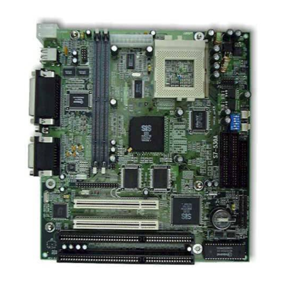
Page 12: S7-530A Detailed Layout
Installation S7-530A S7-530A Detailed Layout 3.5V 3.2V 2.9V 2.8V 2.4V 2.2V 2.1V Winbond 83877 I/Oset CPU FAN Chassis FAN SIS530 PCIset FDD1 IDE1 IDE2 CD2 CD1 POWER_ON J7:WOL KEYLOCK PCI Slot #1 5595 PCIset PCI Slot #2 RESET ISA Slot #1... -
Page 13: Easy Installation Procedure
S7-530A Installation Easy Installation Procedure The following must be completed before powering on your new system: 3-1. Configure DIP Switch and Jumper to match your hardware 3-2. Install memory chips 3-3. Device Connectors Section 3-1 Configure DIP Switch We design this motherboard with a DIP Switch to make your installation fast and easy. -
Page 14: System Memory Configuration
S7-530A Section 3-2 System Memory Configuration Memory Layout The S7-530A supports (2) 168-pin DIMMs (Dual In-line Memory Module). The DIMMs can be either EDO (Enhanced Data Out) or SDRAM (Synchronized DRAM). • DIMM SDRAM may be 83MHz (12ns), 100MHz (10ns) or 125MHz (8ns) bus speed. -
Page 15: Dimm Module Installation
S7-530A Installation DIMM Module Installation Figure 3 displays the notch marks and what they should look like on your DIMM memory module. DIMMs have 168-pins and two notches that will match with the onboard DIMM socket. DIMM modules are installed by placing the chip firmly into the socket at a 90 degree angle and pressing straight down (figure 4) until it fits tightly into the DIMM socket (figure 5). - Page 16 Installation S7-530A Figure 5 DIMM Module clip after installation To remove the DIMM module simply press down both of the white clips on either side and the module will be released from the socket. Page 3-6...
-
Page 17: Device Connectors
S7-530A Installation Section 3-3 Device Connectors Please install the motherboard into the chassis. Now that your motherboard is installed you are ready to connect all your connections (figure 6). Joystick/Midi port parallel port PS/2 Mouse USB port PS/2 KEYBOARD COM1... - Page 18 Installation S7-530A Section3-4 Device Connectors (continued) KeyLock - Keyboard lock switch & Power LED connector 1. Power LED(+) 4. Keylock 2. N/C 5. GND 3. GND Speaker - Connect to the system's speaker for beeping 1. Speaker 3. GND 2. N/C 4.
-
Page 19: Standard Cmos Setup
S7-530A BIOS Award’s ROM BIOS provides a built-in Setup program which allows user to modify the basic system configuration and hardware parameters. The modified data will be stored in a battery-backed CMOS, so that data will be retained even when the power is turned off. - Page 20 BIOS S7-530A The menu displays all the major selection items. Select the item you need to reconfigure. The selection is made by moving the cursor (press any direction key ) to the item and pressing the ‘Enter’ key. An on-line help message is displayed at the bottom of the screen as the cursor is moved to various items which provides a better understanding of each function.
- Page 21 S7-530A BIOS NOTE: The “Halt On:” field is used to determine when to halt the system by the BIOS if an error occurs. NOTE: Floppy 3 Mode support is a mode used to support a special 3.5” drive used in Japan. This is a 3.5” disk that stores only 1.2 MB, the default setting for this is disabled.
- Page 22 BIOS S7-530A Enabled: Activates automatically when the system boots up causing a warning message to appear when anything attempts to access the boot sector. Disabled: No warning message will appear when anything attempts to access the boot sector. Note: Many disk diagnostic programs that access the boot sector table can trigger the virus warning message.
- Page 23 S7-530A BIOS Swap Floppy Drive: This will swap your physical drive letters A & B if you are using two floppy disks. The default is Disabled. Enabled: Floppy A & B will be swapped under the O/S. Disabled: Floppy A & B will be not swapped.
- Page 24 BIOS S7-530A Typematic Delay (msec): This setting controls the time between the first and the second character displayed by typematic auto-repeat. The default is 250. 250: 250 msec. 500: 500 msec. 750: 750 msec. 1000: 1000 msec. Security Option: This category allows you to limit access to the System and Setup, or just to Setup.
- Page 25 S7-530A BIOS YES: Report FDD for WIN95 Video BIOS Shadow: This option allows video BIOS to be copied into RAM. Video Shadowing will increase the video performance of your system. The default is Enabled. Enabled: Video shadow is enabled. Disabled: Video shadow is disabled.
- Page 26 BIOS S7-530A Choose the “CHIPSET FEATURES SETUP” in the CMOS SETUP UTILITY menu to display following menu. ROM PCI/ISA BIOS(2A5IMPA9) CHIPSET FEATURES SETUP AWARD SOFTWARE, INC. Refresh Rate Control : 15.6us System BIOS Cacheable : Disabled Ref/Act Command Delay : 6T...
- Page 27 S7-530A BIOS Ras Precharge Time: The precharge time is the number of cycles it takes for the RAS to accumulate its charge before DRAM refreshes. If insufficient time is allowed, refresh may be incomplete and the DRAM may fail to retain data.
- Page 28 BIOS S7-530A SDRAM WR Retire Rate: The system designer must select the correct timing for data transfers from the write buffer to memory, according to DRAM specifications. The default is X-1-1-1. The choice: 0WS, 1WS DRAM Opt RAS Precharge: The precharge time is the number of cycles it takes for the RAS to accumulate its charge before DRAM refreshes.
- Page 29 S7-530A BIOS AGP Aperture Size: The amount of system memory that the AGP card is allowed to share. The default is 64. 4: 4MB of systems memory accessable by the AGP card. 8: 8MB of systems memory accessable by the AGP card.
- Page 30 BIOS S7-530A Auto Detect DIMM/PCI Clk: Allows you to stop DIMM/PCI Clock drive when the DIMM site or PCI Slot are not plug. This item may help reduce EMI. The default is Enabled. Enabled: Provides unused DIMM/PCI to stop. Disabled: Provides the clock generator always driving.
- Page 31 S7-530A BIOS ACPI Function: This option allows you to select ACPI Function. The default is Enabled. Enabled: Support ACPI function for new O.S Disabled: No Support ACPI function. Power Management: Use this to select your Power Management selection. The default is User define.
- Page 32 9: IRQ 9 10: IRQ 10 11: IRQ 11 The S7-530A supports HDD Power Down, Doze and Standby power saving func- tions when using the Intel Pentium II Processor. The default is Disabled Hot Key Power Off: Select Enabled if your system has a hot key for soft power off.
- Page 33 S7-530A BIOS Doze Mode: When enabled and after the set time of system inactivity, the CPUclock will run at slower speed while all other devices still operate at full speed. Standby Mode: When enabled and after the set time of system inactivity, the fixed disk drive and the video would be shut off while all other devices still operate at full speed.
- Page 34 BIOS S7-530A IRQ 8 Break Suspend: You can Enabled or Disabled monitoring of IRQ8 (the Real Time Clock) so it does not awaken the system from Suspend mode. Power Button Over Ride: You could press the power button for more than 4 seconds forces the system to enter the Soft-Off state when the system has “hung”.
- Page 35 S7-530A BIOS The PNP/PCI configuration program is for the user to modify the PCI/ISA IRQ signals when various PCI/ISA cards are inserted in the PCI or ISA slots. WARNING: Conflicting IRQ’s may cause the system to not find certain devices.
- Page 36 BIOS S7-530A PCI IRQ Activated: This sets the method by which the PCI bus recognizes that an IRQ service is being requested by a device. Under all circumstances, you should retain the default configuration unless advised otherwise by your system’s manufacturer.
- Page 37 S7-530A BIOS ROM PCI/ISA BIOS(2A5IMPA9) INTEGRATED PERIPHERALS AWARD SOFTWARE, INC. Internal PCI/IDE : Both Onboard Parallel Mode : ECP/EPP IDE Primary Master PIW : Auto ECP Mode Use DMA IDE Primary Slave PIO : Auto Parallel Port EPP Type : EPP1.9...
- Page 38 BIOS S7-530A IDE Secondary Master PIO: The default is Auto. Auto: BIOS will automatically detect the Onboard Secondary Master PCI IDE HDD Accessing mode. Mode 0~4: Manually set the IDE Programmed interrupt mode. IDE Secondary Slave PIO: The default is Auto.
- Page 39 S7-530A BIOS Enabled: Enabled IDE HDD Block Mode. Provides higher HDD transfer rates. Disabled: Disable IDE HDD Block Mode. Onboard FDD Controller: This controls the state of the onboard floppy controller. The default value is Enabled. Enabled: Enable the Onboard Winbond Chips’s floppy drive interface controller.
- Page 40 BIOS S7-530A Onboard Parallel port: This field allows the user to configure the LPT port. The default is 378 / IRQ7. 378H: Enable Onboard LPT port and address is 378H and IRQ7. 278H: Enable Onboard LPT port and address is 278H and IRQ5.
- Page 41 S7-530A BIOS To change the password, choose the “SUPERVISOR PASSWORD or USER PASSWORD” option from the CMOS SETUP UTILITY menu and press [Enter]. NOTE: Either “Setup” or “System” must be selected in the “Security Option” of the BIOS FEATURES SETUP menu.
- Page 42 BIOS S7-530A password and store new one in CMOS RAM. A maximum of 8 characters can be entered. The “IDE HDD auto detection” utility is a very useful tool, especially when you do not know which kind of hard disk type you are using. You can use this utility to detect the correct disk type installed in the system automatically.
- Page 43 S7-530A BIOS 1024, 16 & 63 no. Cylinder (1024) x no. Head ( 16) x no. Sector ( 63) x no. per sector ( 512) 528 Megabytes If user set his HDD to NORMAL mode, the maximum accessible HDD size will be...
- Page 44 BIOS S7-530A Maximum HDD size: no. Cylinder (1024) x no. Head ( 32) x no. Sector ( 63) x bytes per sector ( 512) 1 GigaByte Note: To support LBA or LARGE mode of HDDs, there must be some software involved. All the software is located in the Award HDD Service Routine (INT 13h).
-
Page 45: Appendix
S7-530A Appendix Appendix A: A-1 MEMORY MAP Address Range Size Description [00000-7FFFF] 512K Conventional memory [80000-9FBFF] 127K Extended Conventional memory [9FC00-9FFFF] Extended BIOS data area if PS/2 mouse is installed [A0000-C7FFF] 160K Available for Hi DOS memory [C8000-DFFFF] Available for Hi DOS memory and adapter ROMs... -
Page 46: Timer & Dma Channels Map
Appendix S7-530A [3D0-3DF] CGA adapter. [3F0-3F7] FLOPPY DISK controller. [3F8-3FF] SERIAL port 1. A-3 TIMER & DMA CHANNELS MAP TIMER MAP: TIMER Channel 0 System timer interrupt. TIMER Channel 1 DRAM REFRESH request. TIMER Channel 2 SPEAKER tone generator. DMA CHANNELS: DMA Channel 0 Available. -
Page 47: Rtc & Cmos Ram Map
S7-530A Appendix Onboard HARD DISK (IDE1) channel. Onboard HARD DISK (IDE1) channel. A-5 RTC & CMOS RAM MAP RTC & CMOS: Seconds. Second alarm. Minutes. Minutes alarm. Hours. Hours alarm. Day of week. Day of month. Month. Year. Status register A. - Page 48 Appendix S7-530A Page Left Blank...
-
Page 49: Post Codes
S7-530A Appendix Appendix B: B-1 POST CODES ISA POST codes are typically output to I/O port address 80h. POST (hex) DESCRIPTION 01-02 Reserved. Turn off OEM specific cache, shadow. 1. Initialize EISA registers (EISA BIOS only). 2. Initialize all the standard devices with default values Standard devices includes. - Page 50 Appendix S7-530A Initialization of the BIOS Data Area. (40:ON - 40:FF) 1. Program some of the Chipset's value according to Setup. (Early Setup Value Program) 2. Measure CPU speed for display & decide the system clock speed. 3. Video initialization including Monochrome, CGA, EGA/VGA. If no display device found, the speaker will beep.
- Page 51 S7-530A Appendix Try to turn on Level 2 cache. Note: Some chipset may need to turn on the L2 cache in this stage. But usually, the cache is turn on later in POST 61h. 3F-40 Reserved. 1. Program the rest of the Chipset's value according to Setup.
-
Page 52: Unexpected Errors
Appendix S7-530A 1. Try to turn on Level 2 cache. Note: If L2 cache is already turned on in POST 3D, this part will be skipped. 2. Set the boot up speed according to Setup setting. 3. Last chance for Chipset initialization. -
Page 53: Load Setup Defaults
S7-530A Appendix Appendix C NOTE: The "LOAD SETUP DEFAULTS" function loads the system default data directly from ROM and initializes the associated hardware properly. This function will be necessary when you accept this mainboard, or the system CMOS data is corrupted.
Need help?
Do you have a question about the S7-530A and is the answer not in the manual?
Questions and answers