Chapters
Table of Contents

Subscribe to Our Youtube Channel
Related Manuals for Ziatech Corporation ZT 8808A


Summary of Contents for Ziatech Corporation ZT 8808A
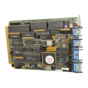
- Page 1 ZT 8808A/8809A V20 Single Board Computers OPERATING MANUAL ZT 8808A/8809A REVISION A ZT 88CT08A/88CT09A REVISION A May 1, 1993 1050 Southwood Drive San Luis Obispo, CA 93401 USA FAX (805) 541-5088 Telephone (805) 541-0488...
- Page 2 Life Support Policy: Ziatech products are not authorized for use as critical components in life support devices or systems without the express written approval of the president of Ziatech Corporation. As used herein: 1. Life support devices or systems are devices or systems that...
- Page 3 CUSTOMER SUPPORT If you have a technical question, please call Ziatech’s Customer Support Service at one of the following numbers. Corporate Headquarters: (805) 541-0488 (805) 541-5088 (FAX) You can also use a modem to leave a message on the 24-hour Ziatech Bulletin Board...
- Page 4 PC viable for compact industrial applications. This manual describes the operation and use of the ZT 8808A/8809A. The only difference between the ZT 8808A and ZT 8809A is the processor clock speed; the ZT 8808A runs at 5 MHz and the ZT 8809A runs at 8 MHz.
- Page 5 Preface STD bus compatibility, serial communications, interrupts, direct memory access, power-fail protection, and battery backup. Chapter 4, "Application Examples," provides specific examples of the ZT 8809A in operation, including code to implement these applications. The examples demonstrate the use of interrupts, timers, and the real-time clock.
- Page 6 (PIC). Chapter 13, "ZT 88CT08A/88CT09A CMOS Boards," describes the functional, electrical, and environmental characteristics of the CMOS versions of the ZT 8808A and ZT 8809A that differ from the non-CMOS versions. Appendix A, "Jumper Configurations," describes the ZT 8809A jumper selectable options in detail.
-
Page 7: Table Of Contents
CONTENTS INTRODUCTION Chapter 1. INTRODUCTION OVERVIEW ........... . . ZT 88CT08A and ZT 88CT09A . - Page 8 ............CMOS VERSIONS OF THE ZT 8808A/8809A 3-27 .
- Page 9 Contents Chapter 4. APPLICATION EXAMPLES OVERVIEW ........... . . EXAMPLE 1-A: USING SIMPLE INTERRUPTS .
- Page 10 Contents Prefetch Pointer (PFP) ........General Purpose Registers .
- Page 11 Contents Line Status Register 8-26 ......... Interrupt ID Register 8-28 .
- Page 12 Contents Chapter 12. INTERRUPT CONTROLLER (8259A) 12-1 OVERVIEW 12-3 ........... . I/O PORT ADDRESSES 12-3 .
- Page 13 ........ZT 8808A/8809A REVISION HISTORY .
- Page 14 TABLES Table 3–1 Processor Speed Comparison......Table 3–2 Serial Communications Standards..... Table 5–1 Memory Configurations, 3D1/5D1/BRAM.
- Page 15 Tables Table B–9 J5 Pin Assignments. B-17 ....... . Table B–10 J6 Pin Assignments.
- Page 16 ILLUSTRATIONS Figure 1–1 ZT 8809A Functional Block Diagram....Figure 2–1 Non-DOS Factory Default Jumper Configuration..Figure 2–2 ZT 8809A Configured For STD DOS.
- Page 17 Illustrations Figure 11–3 Control Word Format. 11-7 ......Figure 11–4 Counter Latch Command Format. 11-9 .
-
Page 18: Introduction
... OVERVIEW The 5 MHz ZT 8808A and 8 MHz ZT 8809A are 16-bit single board computers (SBCs) designed with DOS applications on the STD bus in mind. The high level of integration allows for a complete STD DOS system on one board. - Page 19 However, systems with large RAM and PROM disks on the ZT 8825 will probably still require the ZT 8825. Peripherals on the ZT 8808A and ZT 8809A include three counter/timers, an interrupt controller, a real-time clock, two RS-232-C serial ports (one of which may be configured to be RS-485), a Centronics printer interface or general purpose parallel I/O port, and four 32-pin memory sockets.
-
Page 20: Zt 88Ct08A And Zt 88Ct09A
ZT 8808A and ZT 8809A, respectively. They are designed for extended temperature and low power applications. All references in this manual to the ZT 8808A and ZT 8809A are also appropriate for the ZT 88CT08A and ZT 88CT09A. Refer to Chapter 13 for information pertaining specifically to the ZT 88CT08A and ZT 88CT09A. -
Page 21: Features Of The Zt 8809A
Introduction FEATURES OF THE ZT 8809A • STD-80 and STD 32 bus compatible • Optional CMOS versions available • 8088/8086 code compatible • Four 32-pin memory sockets, configurable for – 1 EPROM and 3 RAMs or – 2 EPROMs and 2 RAMs •... -
Page 22: Figure 1-1 Zt 8809A Functional Block Diagram
Introduction ZT 8809A RS-232-C Counter/ Serial Timers Centronics Optional Printer Battery Backup RS-232-C/ Interrupt RS-422/485 Controller Serial Clock 32K RAM AC/DC Real-time Slowdown (Optional Power- Clock Battery Fail Halt/ Backup) Restart 256K RAM & 256K ROM 384K RAM & 128K ROM (RAM Optionally Battery-backed) Figure 1–1. -
Page 23: Functional Blocks
Introduction FUNCTIONAL BLOCKS Figure 1-1 illustrates the ZT 8809A’s functional blocks. A brief description of each block follows. V20 (uPD70108) Processor The NEC V20 is an 8088-compatible microprocessor with a 16-bit internal data bus and an 8-bit external data bus. The V20 executes all code written for the 8088/8086 family of microprocessors and includes a superset of their instruction set. -
Page 24: Wait-State Generator
Introduction Wait-State Generator To accommodate I/O and memory boards needing more time for access, the ZT 8809A contains a one wait-state generator. If enabled, it inserts one wait-state (clock cycle) within the normal four-clock bus cycle to increase it to five clocks. This gives memory and I/O boards additional time between address valid time and the end of the bus cycle to complete an access. -
Page 25: Ac/Dc Power-Fail Detection
Introduction Jumpers are provided to select whether the following three groups of devices, either individually or as a whole, are to be battery-backed: • Real-time clock and 32 Kbyte RAM • Two RAM sockets • ROM/RAM socket when RAM is present This conserves battery power exclusively for those devices that require backup. -
Page 26: Real-Time Clock
Introduction Real-Time Clock The real-time clock on the ZT 8809A is a Dallas Semiconductor DS 1215. It keeps track of hundredths of seconds, seconds, minutes, hours, days, date of the month, months, and years. The clock automatically corrects for leap years, and adjusts for months with fewer than 31 days. -
Page 27: Counter/Timers
Introduction Counter/Timers The ZT 8809A has three independent 16-bit counter/timers, each of which can be used as a timer or event counter. The clock frequency driving each of these timers is a 1.19318 MHz oscillator. For timers 1 and 2, the clock input may be jumpered to receive the frontplane connector J4 signal, which may be an external frequency or event input. -
Page 28: Interrupts
Introduction Interrupts The programmable interrupt controller (PIC) on the ZT 8809A is an Intel 8259A-2 or equivalent. It has eight interrupt inputs that can be prioritized in software. Its output drives the CPU interrupt input. All PIC interrupt inputs may be jumper selected between various on- board sources and the five frontplane and three backplane sources. -
Page 29: Centronics Printer/General Purpose I/O Port
Introduction Centronics Printer/General Purpose I/O Port A Centronics printer interface is included on the ZT 8809A. It may drive a Centronics-compatible printer directly. The printer interface can also be used for general purpose I/O. It consists of eight I/O lines for data, four open collector I/O lines for control, and five input lines for status. -
Page 30: Clock Slowdown & Halt Restart (Cmos Boards Only)
Introduction Clock Slowdown & Halt Restart (CMOS boards only) For power conservation, the ZT 88CT08A and ZT 88CT09A contain two features to slow down or stop processor execution program- matically. These are the clock slowdown and halt with interrupt restart features, provided by a special Harris Semiconductor 82C85 clock chip that replaces the 82C84A normally shipped on the ZT 8809A board. -
Page 31: Getting Started
Chapter 2 GETTING STARTED Contents Page OVERVIEW ........... . . UNPACKING . -
Page 32: Overview
ZT 8809A into an STD bus card cage. You should read this chapter and Chapter 3, "Theory of Operation," before you attempt to use the board. Remember, unless specifically stated otherwise, all references to the ZT 8809A also pertain to the ZT 8808A, ZT 88CT08A, and ZT 88CT09A. UNPACKING Please check the shipping carton for damage. - Page 33 ZT 8809A, refer to the software manual for a list of the items that should be included. • ZT 8808A or ZT 8809A Single Board NEC V20 Computer or ZT 88CT08A or ZT 88CT09A Single Board 80C88 Computer. • ZT 8808A/8809A Operating Manual (in binder) •...
-
Page 34: Physical Requirements
Appendix B for board dimensions with and without the zSBC 337 module attached. Power Requirements Power requirements for the ZT 8808A and ZT 8809A are +5 VDC at 1.6 A maximum, 0.8 A typical. For serial communications, the requirements are +12 VDC at 24 mA maximum and -12 VDC at 24 mA maximum. - Page 35 Getting Started Important Note: The ZT 8809A CPU uses an 82C84A or 82C84B as the clock generator. The following special considerations should be observed regarding the +5 VDC power supply: • The +5 VDC power supply should never have a rise time faster than 1 V per millisecond.
-
Page 36: Environmental Requirements
Getting Started Environmental Requirements The ambient temperature must be maintained at 0˚ to +65˚ Celsius for proper operation and to avoid possible damage to the ZT 8809A (the ZT 88CT08A and ZT 88CT09A allow for a lower power requirement and wider temperature range, detailed in Chapter 13). Relative humidity should be less than 95% at 40˚... -
Page 37: Installing The Zt 8809A
Getting Started INSTALLING THE ZT 8809A The fastest way to begin using the ZT 8809A is with the addition of development software available from Ziatech. The STD ROM development system allows you to download application software developed on an IBM PC (or equivalent) through a serial port onto the ZT 8809A. -
Page 38: Figure 2-1 Non-Dos Factory Default Jumper Configuration
Getting Started INTERRUPTS TIMER COUNTER COM2 COM1 Figure 2–1. Non-DOS Factory Default Jumper Configuration. -
Page 39: Configuring The Zt 8809A For Std Rom
Getting Started Configuring the ZT 8809A for STD ROM The STD ROM development system is available as an option to the ZT 8809A for software development. If STD ROM is ordered along with the ZT 8809A, the board is preconfigured and tested at the factory prior to shipment. -
Page 40: Std Rom Cable Requirements
Getting Started STD ROM Cable Requirements A serial link is required for the STD ROM system between frontplane connector J1 and the IBM PC or compatible. The cable shipped with the STD ROM system should be used for this purpose. Plug this cable into connector J1 of the ZT 8809A. -
Page 41: Powering Up Std Rom
Getting Started Note: This configures sockets 3D1 and 5D1 for 64 Kbyte ROMs and sockets 7D1 and 9D1 for 128 Kbyte RAMs. Memory mapping information may be found in the jumper configuration tables for W55- W59 in Appendix A. Powering Up STD ROM Once the EPROM, RAM, jumpers, and cable are correctly configured, install the ZT 8809A into the STD bus card cage. - Page 42 Getting Started • Some things to check if the system is not working: 1. Two ZT 8809A frontplane connectors accept the ZT 90014 serial cable. STD ROM works only in serial port 1 at J1. 2. If a PC is used that has more than one 25-pin male connector, be sure the serial cable is plugged into COM1.
-
Page 43: Configuring The Zt 8809A For Std Dos
Getting Started Configuring the ZT 8809A for STD DOS STD DOS is an optional MS-DOS operating system available for the ZT 8809A V20 processor board. If the ZT 8809A and STD DOS are ordered together, Ziatech configures the ZT 8809A properly prior to shipment and tests it as a system. -
Page 44: Figure 2-2 Zt 8809A Configured For Std Dos
Getting Started INTERRUPTS TIMER COUNTER COM2 COM1 Figure 2–2. ZT 8809A Configured For STD DOS. 2-14... -
Page 45: Std Dos Memory Requirements
Getting Started STD DOS Memory Requirements The STD DOS/BIOS software is shipped in one EPROM for installation onto the ZT 8809A at socket location 5D1 (see Figure 2-2). Install the EPROM only at a static-free workstation. Orient pin 1 properly, to the lower left with the board oriented component side up, goldfingers to the left. -
Page 46: Std Dos Cable Requirements
Getting Started STD DOS Cable Requirements If the STD DOS system is not a Stand Alone (SA) system, a serial link is required between the ZT 8809A and a terminal or PC. Refer to the STD DOS System Manual for cabling requirements. The ZT 90039 optional printer cable is available from Ziatech for use with a Centronics printer port. -
Page 47: Powering Up Std Dos
Getting Started Powering Up STD DOS Be sure the ZT 8809A is seated securely into the card cage and the power switch is off. Plug the card cage into your power source. Refer to the following instructions appropriate to your configuration (PC- Assisted with a host computer, PC-Assisted with a terminal or video board, or Automation Engine). - Page 48 Getting Started PC-Assisted with a terminal or video board - The PC-Assisted system can also communicate with a terminal via COM2, or through a Ziatech video board with keyboard support. 1. If you are using a terminal for communication with the ZT 8809A STD DOS system, connect the system’s serial cable from the proper serial port to the terminal.
-
Page 49: Memory Addressing
512 Kbyte RAMs. One of the EPROM sockets may also be config- ured for static RAM. All RAM may be battery-backed. Memory access times required are 380 ns for a ZT 8808A and 210 ns for a ZT 8809A. If DMA to or from on-board memory is used, chip access times remain the same. -
Page 50: Figure 2-3 Std Dos Factory Default Memory Map
Getting Started FFFFFh 256 Kbyte ROM Drive w/ 256 Kbyte EPROM DFFFFh 32 Kbyte RAM Drive and Timekeeper D8000h C0000h 5FFFFh 128 Kbyte ROM Drive w/ 128 Kbyte EPROM 40000h 3FFFFh On-Board RAM w/ 128 Kbyte RAMs Note: Shaded portion represents off-board memory address space. Figure 2–3. -
Page 51: Figure 2-4 Std Rom Factory Default Memory Map
Getting Started FFFFFh 128 Kbytes w/ 64 Kbyte EPROM E0000h DFFFFh 32 Kbyte RAM Drive and Timekeeper D8000h D7FFFh 40000h 3FFFFh On-board RAM w/ 128 Kbyte RAMs Note: Shaded portion represents off-board memory address space. Figure 2–4. STD ROM Factory Default Memory Map. 2-21... -
Page 52: I/O Addressing
Getting Started I/O ADDRESSING Figure 2-5 on page 2-23 shows the I/O addresses occupied by the ZT 8809A, for both STD DOS and STD ROM systems. I/O accesses are made via the full 16-bit I/O address, allowing for 64 Kbytes of I/O addresses. Eight-bit I/O boards are also compatible with the ZT 8809A, provided the equivalent 8-bit addresses occupied by the on-board devices are avoided. -
Page 53: Figure 2-5 I/O Map, Std Dos / Std Rom Systems
Getting Started FFFFh 0400h 03FFh Serial Port 1 (COM 1) 03F8h 03F7h 0380h 037Fh Printer Port 1 (LPT 1) 0378h 0377h 0300h 02FFh Serial Port 2 (COM 2) 02F8h 02F7h 0048h 0047h 8254 Timers 0040h 003Fh 0028h 0027h 8259A Interrupt Controller 0020h 001Fh... -
Page 54: Upgrading From Zt 8806/8807 Systems
Getting Started UPGRADING FROM ZT 8806/8807 SYSTEMS If you are upgrading your existing STD DOS system from ZT 8806/8807 boards to the ZT 8809A DOS systems, you should be aware of the enhancements introduced with the ZT 8809A DOS that may affect compatibility with existing systems. - Page 55 Getting Started These changes affect the ZT 8844 EGA keyboard controller to the extent that the Revision A board is not compatible with the ZT 8809A DOS system. A modified version designated ZT 8844-III Rev. A, or ZT 8844 Rev. B or later, should be ordered with ZT 8809A DOS systems.
- Page 56 ............CMOS VERSIONS OF THE ZT 8808A/8809A 3-27 .
-
Page 57: Overview
Theory of Operation OVERVIEW This chapter describes the following system level issues: • Processor performance compared to the IBM PC/XT® • STD bus compatibility • Serial communications using RS-232-C or RS-422/485 • Expanding the ZT 8809A interrupt structure • Direct Memory Access (DMA) support and benefits •... -
Page 58: Relative Microprocessor Performance
RELATIVE MICROPROCESSOR PERFORMANCE Norton’s System Information version 4.50 was used to measure the ZT 8808A and ZT 8809A processor performance relative to that of the IBM PC. The test compared several processing tasks; the test results are presented in Table 3-1. -
Page 59: Std Bus Compatibility
Theory of Operation STD BUS COMPATIBILITY The ZT 8809A is fully compatible with Revision 2.3 of the STD-80 Series Bus Specification. This revision of the bus specification includes definition of two new backplane interrupt request signals, INTRQ1* and INTRQ2*, which replace the signals RESERVED and CNTRL*, respectively. -
Page 60: Serial Port 1 (Com1)
Theory of Operation Serial Port 1 (COM1) The programming architecture of both serial ports 1 and 2 is the same as for the popular WD 8250. The baud rate generator is integral to the serial controller, configurable for a range of baud rates up to 56 Kbaud. -
Page 61: Serial Port 2 (Com2)
Theory of Operation Serial Port 2 (COM2) Serial ports 1 and 2 are identical in features and programming with respect to RS-232-C communication, with one exception. You can disable serial port 2 by removing jumper W66. This is useful for systems adding a modem card at the same I/O address as on the ZT 8809A. -
Page 62: Theory Of Operation
Theory of Operation Table 3-2 Serial Communications Standards. Parameter RS-232-C RS-423-A RS-422-A RS-485 Operation Single-ended Single-ended Differential Differential Number Of Drivers/Receivers 1/10 1/10 32/32 Maximum Cable Length (Ft.) 4000 4000 4000 Maximum Data Rate † (Bits per second) 100K † The ZT 8809A maximum data rate is limited to 56 Kbaud by the UART A terminated twisted pair should be used to protect the integrity of the RS-485 signals. -
Page 63: Interrupts
Theory of Operation INTERRUPTS The ZT 8809A supports both maskable and non-maskable interrupts. This section discusses system level issues related to these interrupts. Refer to Chapter 12 for more information on the operation and programming of the maskable interrupt controller. Interrupt Request Assignments The 8259A Programmable Interrupt Controller (PIC) on board the ZT 8809A has eight interrupt input requests, each with two... -
Page 64: Figure 3-1 Pic Interrupt Input Requests
Theory of Operation Jumper Selections Interrupt Level 8087 Interrupt † Timer 0 † INTRQ1* FP1/ † INTRQ* Timer 2 FP3/ † COM2* Timer 1 † COM1* Power Fail/ W2,W9 † FP5/ INTRQ2* W3,W10 † FP6/ LPT1 † FP7/ Figure 3–1. PIC Interrupt Input Requests. -
Page 65: Polled Interrupts On The Std Bus
Theory of Operation Polled Interrupts on the STD Bus The PIC can be programmed to supply a unique vector for each of these interrupt inputs. This means only one STD bus interrupt per request can be uniquely defined as shown in Figure 3-2. Since STD DOS expects the use of INTRQ1* and INTRQ2* for particular I/O devices, this leaves only the INTRQ* signal for all remaining I/O devices in the system. -
Page 66: Figure 3-2 Polled Interrupt Structure
Theory of Operation STD BUS INTRQ* INTRQ* ZT 8808A/ INTERRUPT ZT 8809A SOURCE 1 INTAK* INTAK* INTRQ* INTERRUPT SOURCE 2 INTAK* INTRQ* INTERRUPT SOURCE N INTAK* INTERRUPT STATUS PORT Figure 3–2. Polled Interrupt Structure. 3-11... -
Page 67: Std Bus Vectored Interrupts
This number may be decreased if STD DOS is present on the ZT 8809A. STD BUS INTRQ* INTRQ* INTERRUPT ZT 8808A/ SOURCE 1 ZT 8809A INTAK* INTAK* INTRQ* INTERRUPT... -
Page 68: Std Bus Cascaded Interrupts
The system is illustrated in Figure 3-4. STD BUS INTRQ* INTRQ* UP TO INTAK* INTAK* EIGHT INTERRUPT ZT 8808A/ INTER- SOURCE ZT 8809A RUPTS INTRQ* UP TO INTERRUPT EIGHT SOURCE... -
Page 69: Non-Maskable Interrupts
Theory of Operation a unique vector. If STD DOS is installed, this number decreases depending upon the number of devices in the system. Non-Maskable Interrupts In addition to the eight interrupt inputs at the interrupt controller, the ZT 8809A supports three sources of interrupt referred to as "non- maskable"... -
Page 70: Direct Memory Access (Dma)
Theory of Operation DIRECT MEMORY ACCESS (DMA) The ZT 8809A supports Direct Memory Access (DMA) transfers between local memory and STD bus system memory or I/O under the supervision of an STD bus DMA controller. The following discussion covers system level issues of DMA transfers: the advantages and the operation of an STD bus DMA controller with respect to the CPU. -
Page 71: Dma Operation
Theory of Operation DMA Operation Figure 3-5 shows the interface between the ZT 8809A and an STD bus DMA controller. The signals shown are required for proper operation of devices on the STD bus during DMA cycles. The DMA cycle is initiated when the controller asserts the bus request signal BUSRQ* on the STD bus. -
Page 72: Figure 3-5 Dma With Std Bus Controller
Theory of Operation A0-A19 D0-D7 ZT 8808A/ STD BUS I/O OR BUSRQ* MEMORY WITH DMA ZT 8809A BUSAK* MEMRQ* MCSYNC* Figure 3–5. DMA With STD Bus Controller. 3-17... -
Page 73: Power-Fail Protection
Theory of Operation POWER-FAIL PROTECTION The ZT 8809A supports both DC and AC power-fail protection. Advantages of each, as well as operation of both types of power-fail protection, are described in this section. DC Power-Fail The factory default setting enables the ZT 8809A to detect 5 VDC and assert a System Reset if power falls below 4.75 VDC. -
Page 74: Ac Power-Fail
Theory of Operation AC Power-Fail All the logic required to detect AC power failure is present on the ZT 8809A except the AC converter. This converter is available from Ziatech as part number ZT 90071. One end of the converter plugs into the same AC source as the power supply to monitor AC to the STD system. - Page 75 Theory of Operation The advantage of AC power-fail detection is that it provides early warning of impending DC power failure. When jumper W1 is installed, a non-maskable interrupt (NMI) is sent to the processor when AC power below 95 VAC is detected. Alternatively, a maskable interrupt on level 5 (IR5) may indicate the AC power failure when jumper W1 is removed and W9A is installed.
- Page 76 Theory of Operation To detect AC power failure, the ZT 8809A may use any AC converter that provides transformer isolated AC voltage of no more than 30 VAC from the same source that provides power to the STD system. The detection circuitry on board the ZT 8809A is calibrated at the factory to generate an interrupt at 95 VAC RMS with the optional transformer available from Ziatech.
-
Page 77: System Battery Fail
Theory of Operation System Battery Fail For systems whose power is generated entirely from a large battery, the AC power-fail detection circuit may be useful to generate an early warning of battery failure. This warning should take place before the system battery voltage to the ZT 8809A falls below 4.75 V, at which time the system would reset. -
Page 78: Battery
Theory of Operation BATTERY The ZT 8809A contains a socket for an optional 1 Amp-hour 3.9 V lithium battery. As described above, the real-time clock and 32 Kbyte static RAM are protected by the battery if jumper W12 is installed. Jumpers allow the RAM sockets and the configurable RAM/EPROM socket (when configured for RAM) also to be battery-backed. - Page 79 Theory of Operation b) Minimum Data Retention Time: Total Current Drain = Clock + RAM + Buffer 1 uA + 50 uA + 80 uA = 111 uA Battery Life = 1 AHr 1 Day ----- (24-8)Hr 111 uA = 563 Days (1.5 years) 2.
-
Page 80: Status Indicator (Led)
Theory of Operation STATUS INDICATOR (LED) The ZT 8809A includes an LED near the extractor for general purpose use. It is turned on by writing a logical 1 to bit 1 of the printer port Control register at I/O address 037Ah, and is turned off by writing a logical 0 to bit 1 of the same address. -
Page 81: Reset
Theory of Operation RESET The ZT 8809A is equipped with a System Reset circuit that asserts the STD bus SYSRESET* signal at any time DC voltage is less than 4.75 V. It also drives the SYSRESET* signal during the time a pushbutton switch drives the PBRESET* STD bus signal to the ZT 8809A. -
Page 82: Cmos Versions Of The Zt 8808A/8809A
Theory of Operation CMOS VERSIONS OF THE ZT 8808A/8809A The ZT 8808A and ZT 8809A processor boards are also available in CMOS versions, ZT 88CT08A and ZT 88CT09A, respectively. These versions provide lower power and extended temperature operation. Like the ZT 8808A and ZT 8809A, the ZT 88CT08A and ZT 88CT09A differ only in their processor clock speeds;... - Page 83 Theory of Operation Clock Slowdown Power consumption for CMOS logic is directly proportional to the switching speed of the device. The higher the clock frequency, the greater the power dissipation. In order to minimize the power consumption on the ZT 88CT09A boards, the Clock Slowdown feature has been included to allow dynamic switching of the processor clock speed between the normal frequency and that frequency divided by 256.
-
Page 84: Functional Differences
Theory of Operation Halt with Interrupt Restart To further decrease power consumption from the Clock Slowdown mode described above, the processor clock may be halted during times processing is not needed, and restarted by an interrupt. This interrupt may be from an external source, such as an event requiring service from the processor, or from one of the on-board timers. -
Page 85: Chapter 4. Application Examples
Chapter 4 APPLICATION EXAMPLES Contents Page OVERVIEW ........... . . EXAMPLE 1-A: USING SIMPLE INTERRUPTS . -
Page 86: Overview
Application Examples OVERVIEW The following examples show simple uses of some of the more complex devices on the ZT 8809A board. Each example is described first by an outline of the objectives, followed by the software in outline form. The first example is divided into two parts: the first part shows the use of the programmable interrupt controller and the minimum steps required to handle one interrupt from the on-board timer;... -
Page 87: Example 1-A: Using Simple Interrupts
Application Examples EXAMPLE 1-A: USING SIMPLE INTERRUPTS Objectives • Write a software routine that initializes the 8259A Interrupt Controller on board. • Initialize the pointer to the interrupt service routine for the interrupt used. • Provide the framework for an interrupt service routine. The example shown strobes the LED after a certain timeout interrupt provided by the timer 2. -
Page 88: Software Outline
Application Examples Software Outline INITPIC Routine BEGIN Initialize the Interrupt Controller Send ICW1 - Edge triggered, Single, ICW4 needed Send ICW2 - Vector addresses 8 - 15 Send ICW3 - No slave interrupt controllers Send ICW4 - SFNM, Buffered Master, Normal EOI, 8088 Send OCW1 - Unmask all interrupts for STD DOS use Initialization of the Interrupt Vector... - Page 89 Application Examples LED_STROBE routine BEGIN Check state of LED Set it to the opposite state Send End of Interrupt (EOI) byte to PIC Return from ISR INIT_TMR2 Routine BEGIN Send Control byte - set for Mode 2 as a Rate Generator Send low byte of count Send high byte of count MAIN Program...
-
Page 90: Program Code
Application Examples Program Code ;********************************************************** PROGRAMMING ABSTRACT ;********************************************************** SHAWN SHURICK 6/30/88 ZIATECH CORP. SAN LUIS OBISPO, CA ; THIS PROGRAMMING EXAMPLE IS FOR THE ZT 8809A CPU BOARD. IT IS INTENDED TO DEMONSTRATE THE USE OF THE 8259A INTERRUPT CONTROLLER TOGETHER WITH A COUNTER/TIMER. INITIALIZATION OF THE 8259A AND THE INTERRUPT VECTOR IS SHOWN, ALONG WITH INITIALIZATION OF THE COUNTER/ TIMER 2. - Page 91 Application Examples ;*********************************************************** SYSTEM EQUATES ;*********************************************************** * ZT 8809A 8259A REGISTER EQUATES BY PORT ADDRESS * REG A ICW,OCW2,OCW3,IRR,ISR,IL PORT_A_8809A 0020H ; PORT_A ICW1_8809A 00010001B ; EDGE, CASCADE OCW2_8809A 01100010B ; SPECIFIC EOI FOR IR2 REG B ICW2,3,4,OCW1,IMR PORT_B_8809A 0021H ;...
- Page 92 Application Examples ;*********************************************************** MACRO DEFINITIONS ;*********************************************************** MACRO DX,SRC ;; GET I/O PORT AL,DX ;; INPUT DATA ENDM MACRO DX,DST ;; GET I/O PORT DX,AL ;; OUTPUT DATA ENDM ;*********************************************************** INTERRUPT POINTERS SEGMENT ;*********************************************************** ; INTERRUPT POINTER TABLE LOCATED AT 0H INT_POINTERS SEGMENT TYPE_0...
- Page 93 Application Examples ;*********************************************************** STACK SEGMENT ;*********************************************************** ; STACK SEGMENT IS LOCATED IN RAM FOR AN ARBITRARY STACK SIZE. STACK SEGMENT STACK 20 DUP (?) ; UNINITIALIZED STACK STACK_TOP LABEL WORD ; OFFSET OF TOS STACK ENDS ;*********************************************************** DATA SEGMENT ;*********************************************************** DATA SEGMENT NO DATA IS USED IN THIS PROGRAM, BUT WOULD RESIDE HERE...
- Page 94 Application Examples ;*********************************************************** INTERRUPT HANDLERS ;*********************************************************** ; ONLY ONE SERIAL INTERRUPT HANDLER IS ILLUSTRATED. OTHER HANDLERS CAN BE ADDED HERE AS NEEDED. CODE SEGMENT PARA ASSUME CS:CODE,SS:STACK,DS:DATA,ES:NOTHING LED_STROBE PROC ; THIS PROCEDURE HANDLES THE INTERRUPT GENERATED BY THE TIMER 2 ON THE ZT 8809A. FIRST THE PRINTER PORT BIT THAT CONTROLS THE LED IS READ AND EXTRACTED, THEN INVERTED AND OR’D BACK INTO THE BYTE READ.
- Page 95 Application Examples ;*********************************************************** PROCEDURES ;*********************************************************** INIT_PIC PROC ; THIS PROCEDURE IS CALLED TO INITIALIZE THE 8259A PIC. THE PIC IS INITIALIZED TO: SINGLE MODE, EDGE TRIG- GERED, INTERRUPT TYPES 8 - 15 D FOR IRQS 0-7 RE- SPECTIVELY, 8088 MODE, NORMAL (NON-SPECIFIC) END- OF-INTERRUPT, IRQ LINES 0-7 ENABLED.
- Page 96 Application Examples ;*********************************************************** TEST CODE ;*********************************************************** ; INITIALIZE SEGMENT REGISTER AND STACK POINTER. START: AX,SEG DATA DS,AX AX,SEG STACK SS,AX SP,OFFSET STACK_TOP ; INITIALIZE INTERRUPT VECTORS (TYPE 10 ONLY IS USED). PUSH AX,0 DS,AX DI,OFFSET TYPE_10 CX,1 ; 1 VECTOR TO BE INITIALIZED VECT: WORD PTR [DI],OFFSET LED_STROBE DI,2...
-
Page 97: Example 1-B: Handling Slave Interrupts
Application Examples EXAMPLE 1-B: HANDLING SLAVE INTERRUPTS Objectives • Write a software routine that initializes the 8259A Interrupt Controller on-board to act as a master to receive interrupts from both a slave interrupt controller and on-board devices. • Write a software routine that initializes the 8259A Interrupt Controller on the ZT 8840 Quad UART board to act as a slave interrupt controller. -
Page 98: System Configuration
Application Examples System Configuration The following example assumes that a ZT 8809A and a ZT 8840 are present in the STD bus card cage. All jumpers are assigned in the factory default configuration except the following: 1. ZT 8809A - No jumper changes required. 2. - Page 99 Application Examples Initialize the 8840 Interrupt Controller Send ICW1 - Edge triggered, Cascade, ICW4 needed Send ICW2 - Vector addresses 248 - 255 D Send ICW3 - Slave interrupt controller ID #2 Send ICW4 - SFNM, Buffered Slave, Normal EOI, 8088 Send OCW1 - Unmask interrupt IR0 INIT_VECT Routine BEGIN...
- Page 100 Application Examples SERIAL_8250 Routine BEGIN Indicate to the main program that the interrupt was received Disable further serial interrupts (no more are desired in this program) Send EOI to the ZT 8809A Send EOI to the ZT 8840 Interrupt Controller Return from Interrupt MAIN Program BEGIN...
-
Page 101: Program Code
;*********************************************************** SYSTEM CONFIGURATION ;*********************************************************** ; THE SYSTEM IS ASSUMED TO CONTAIN ONE ZT 8808A OR ZT 8809A, WITH STD DOS SOFTWARE INSTALLED. IN ADDITION, A ZT 8840 IS INSTALLED AT I/O ADDRESS E0H CONFIGURED AS A SLAVE INTERRUPT CONTROLLER. BE SURE NO OTHER CARDS... - Page 102 Application Examples ;*********************************************************** SYSTEM EQUATES ;*********************************************************** ; SET TO 0 FOR STD DOS SYSTEM * ZT 8809A 8259A REGISTER EQUATES BY PORT ADDRESS * REG A ICW,OCW2,OCW3,IRR,ISR,IL PORT_A_8809A 0020H ; PORT A ICW1_8809A 00010001B ; EDGE, CASCADE, ICW4 NEEDED OCW2_8809A 01100010B ;...
- Page 103 Application Examples REG #1 INTERRUPT ENABLE REG (W) PORT_INTEN 001H ; INTERRUPT EN. PORT_DLAMB 001H ; IF DLAB=1, MSB DIV. ERBI ; EN INTR ON RECV EIRBI ; EN INTR ON RECV EIRBO ; EN INTR ON XMT ELSI ; EN LINE STATUS EDSSI ;...
- Page 104 Application Examples REG #6 MODEM STATUS REG (R) PORT_MODS 006H ; MODEM STATUS DCTS ; DELTA CTS DDSR ; DELTA DSR TERI ; TRAIL RING IND. DSLSD ; DELTA RECV SIG. ; CLEAR TO SEND ; DATA SET READY ; RING INDICATOR RLSD ;...
- Page 105 Application Examples TYPE_8 ; 8259A IR0-TIMER 0 TYPE_9 ; 8259A IR1-KEYBD TYPE_10 ; 8259A IR2-TIMER2 (W6B) TYPE_11 ; 8259A IR3-COM2 TYPE_12 ; 8259A IR4-COM1 TYPE_13 ; 8259A IR5-FP5 TYPE_14 ; 8259A IR6-FP6 TYPE_15 ; 8259A IR7-FP7 ; INTERRUPT POINTER TABLE IS LOCATED AT THE TOP END OF 256D INTERRUPT TYPES.
- Page 106 Application Examples ;*********************************************************** INTERRUPT HANDLERS ;*********************************************************** ; ONLY ONE SERIAL INTERRUPT HANDLER IS ILLUSTRATED. OTHER HANDLERS CAN BE ADDED HERE AS NEEDED. CODE SEGMENT PARA ASSUME CS:CODE,SS:STACK,DS:DATA,ES:NOTHING SERIAL_8250 PROC ; THIS PROCEDURE HANDLES INTERRUPTS GENERATED BY THE 8259A PIC ON THE ZT 8840. THE INT_FLAG LOCATION WILL RECORD THAT THE INTERRUPT WAS RECEIVED WITH A ZERO VALUE.
- Page 107 Application Examples ;*********************************************************** PROCEDURES ;*********************************************************** INIT_PIC_8809A PROC ; THIS PROCEDURE IS CALLED TO INITIALIZE THE 8259A PIC. THE PIC IS INITIALIZED TO: SINGLE MODE, EDGE TRIG- GERED, INTERRUPT TYPES 8 - 15 D FOR IRQS 0-7 RE- SPECTIVELY, 8088 MODE, NORMAL (NON-SPECIFIC) END- OF-INTERRUPT, IRQ LINES 0-7 ENABLED.
- Page 108 Application Examples LED_STROBE PROC ; THIS PROCEDURE STROBES THE LED ON THE ZT 8809A, THEREBY INDICATING TO THE USER THE INTERRUPT EXPECTED WAS RECEIVED. FIRST THE PRINTER PORT BIT THAT CONTROLS THE LED IS READ AND EXTRACTED, THEN INVERTED AND OR’D BACK INTO THE BYTE READ. THE BYTE IS THEN REWRITTEN TO THE PRINTER PORT.
- Page 109 Application Examples INIT_UART PROC ; THIS PROCEDURE IS CALLED TO INITIALIZE A UART. THE FOL- LOWING PARAMETERS ARE INITIALIZED: 8-BIT CHARACTER LENGTH 1-START/STOP BIT 9600-BAUD NO PARITY NO INTERRUPTS ; INPUTS: UART - BASE ADDRESS OF UART TO BE INIT ;...
- Page 110 Application Examples ;*********************************************************** TEST CODE ;*********************************************************** ; INITIALIZE SEGMENT REGISTER AND STACK POINTER. START: AX,SEG DATA DS,AX AX,SEG STACK SS,AX SP,OFFSET STACK_TOP ; INITIALIZE INTERRUPT VECTORS PUSH AX,0 DS,AX DI,OFFSET TYPE_248 CX,1 ; 1 VECTOR TO BE INITIALIZED VECT: WORD PTR [DI],OFFSET SERIAL_8250 DI,2 [DI],CS DI,2...
- Page 111 Application Examples AL,EIRBO ; ENABLE DATA TRANSMIT ; INTERRUPT UART1+PORT_INTEN ; AT THE UART INTERRUPT ; ENABLE REG ; ENABLE INTERRUPTS DX,UART1+PORT_LINST ; GET CONSOLE STATUS WAIT_RDY: AL,DX ; INPUT THE STATUS AL,THRE ; CHECK IT FOR TXMIT BUF EMPTY WAIT_RDY ;...
-
Page 112: Example 2: Power-Fail/Watchdog Timer
Application Examples EXAMPLE 2: POWER-FAIL/WATCHDOG TIMER Objectives • Write routines for system initialization and system restart after power-fail. • Write a routine that handles the non-maskable interrupt that may be caused by power-fail. • Write a routine that handles the maskable interrupt from the watchdog timer timeout. -
Page 113: System Requirements
Application Examples System Requirements The following example assumes a ZT 8809A configured with the factory default jumper assignments, with the following exceptions. 1. If detecting AC power failure: • wire-wrap jumper W1 as if installed, and continue the wire to attach to W46B •... - Page 114 Application Examples The following application example is written with both methods of power-fail detection in mind. The flowchart indicates that two different paths may be taken depending on whether the cause is an external battery failure or an AC power failure. If an external battery failure is being detected, it is assumed that the non-maskable interrupt remains until the battery is replaced, so the code goes into an idle loop awaiting battery change.
-
Page 115: Software Outline
Application Examples Software Outline MAIN Program BEGIN Point to battery-backed RAM (segment location DC00h for STD DOS) If "System Data Saved" flag set Then a "warm" start so call RESET routine Else A "cold" start so call INIT routine Remaining code to initialize the software and hardware (including 8259A PIC) that resides here RESET Routine... - Page 116 Application Examples INIT Routine BEGIN Initialize the NMI routine pointer Initialize the segment registers Initialize the software data Initialize the hardware, ie. the 8259A Programmable Interrupt Controller and one of the 8254 Timers to be used as the watchdog timer (use mode 4) Trigger the watchdog timer Return NON-MASKABLE INTERRUPT Service Routine...
- Page 117 Application Examples If yes, halt the system, awaiting system battery replacement (for systems powered by battery only) If no, read SLIN* (bit 3) at the Printer Port Control register at address 037Ah. If set to 1, continue to read the bit and check. Power-fail condition persists.
-
Page 118: Flowcharts For Ac Power-Fail & Watchdog Interrupts
Application Examples Flowcharts For AC Power-Fail & Watchdog Interrupts MAIN PROGRAM START SET ES = BATTERY BACKED RAM (DC00h IS STD DOS DEFAULT) SYSTEM DATA SAVED FLAG SET? MUST BE A WARM MUST BE A COLD START. CALL START. CALL RESET ROUTINE INIT ROUTINE NORMAL MAIN PROGRAM... - Page 119 Application Examples RESET ROUTINE START INITIALIZE THE NMI INTERRUPT POINTER RESTORE CRITICAL PROGRAM DATA RESTORE PROGRAM SEGMENT REGISTERS TRIGGER THE WATCHDOG TIMER CLEAR THE SYSTEM DATA SAVED FLAG RETURN 4-35...
- Page 120 Application Examples INIT ROUTINE START INITIALIZE THE NMI INTERRUPT POINTER INITIALIZE THE SEGMENT REGISTERS INITIALIZE THE SOFTWARE DATA INITIALIZE THE WATCH- DOG TIMER USING ONE 8254 16-BIT TIMER SET TO MODE 4 INITIALIZE THE INTERRUPT CONTROLLER MASKING THE POWER FAIL INTERRUPT LEVEL 5 TRIGGER THE WATCHDOG TIMER RETURN...
- Page 121 Application Examples NON-MASKABLE INTERRUPT SERVICE ROUTINE START TRIGGER THE WATCHDOG TIMER READ INTERRUPT RE- QUEST REGISTER BIT 5 IS IT SET? POWER FAIL NMI OTHER NMI SO CHECK SO DO THE FOLLOWING FOR SOURCES ELSE- WHERE IN THE SYSTEM AND HANDLE THEM SAVE REGISTERS, IE, SEGMENT, AX, BX, CX, DX, SI, DI, BP, SP, IN...
- Page 122 Application Examples POWER FAIL CIRCUIT USED TO DETECT LOW BATTERY SUPPLY VOLTAGE TO SYSTEM? AC POWER FAIL HALT PROCESSOR TO DETECTED AWAIT MAIN BATTERY SUPPLY REPLACEMENT SET SLIN BIT AT PRINTER PORT CONTROL REGISTER ADDRESS 037Ah TO 1 TO ALLOW READ (OPEN COLLECTOR OUTPUT) READ SLIN BIT...
- Page 123 Application Examples THE POWER FAIL CONDITION IS ENDED IT MUST HAVE BEEN A BROWNOUT SITUATION WITH NO HARDWARE RESET REINITIALIZE THE INTER- RUPT CONTROLLER TO CLEAR IRR CALL RESET ROUTINE RETURN FROM INTERRUPT 4-39...
-
Page 124: Example 3: Real-Time Clock Drivers
Application Examples EXAMPLE 3: REAL-TIME CLOCK DRIVERS Objectives • Write the read and write routines which can initialize the time and read it back. • Write the real-time clock access routine, which is required before reading or writing the clock. System Configuration The ZT 8809A must be configured for the factory default jumper assignments for this example. - Page 125 Application Examples WRIT_CLK Routine BEGIN Write 64 bytes of data into the real-time clock Read the real-time clock once to reset the comparison register to be sure it is no longer accessible MAIN Routine BEGIN Call INIT_CLK to be able to access the real-time clock Call WRIT_CLK to write the initial time to the clock (or) Call INIT_CLK to be able to access the real-time clock...
-
Page 126: Chapter 5. Memory And I/O Capability
Chapter 5 MEMORY AND I/O CAPABILITY Contents Page OVERVIEW ........... . . MEMORY ADDRESSING . -
Page 127: On-Board Memory Capacity
Memory and I/O Capability MEMORY ADDRESSING The ZT 8809A processor board is capable of addressing up to 1 Mbyte of memory, both on-board and to the STD bus. This is the maximum memory addressing capability of the V20 and 8088 microprocessors. -
Page 128: Write Protection
Memory and I/O Capability Also included on-board is a 32 Kbyte static RAM, referred to as the H: drive in STD DOS systems prior to BIOS Version 3.0 and the R: drive for BIOS versions of 3.0 and later. This RAM is located in the address space just below the EPROM on board. -
Page 129: Memory Maps
Memory and I/O Capability MEMORY MAPS Figures 5-1 through 5-6 represent some of the possible memory maps for the ZT 8809A, along with jumper configuration drawings. Figures 5-1 and 5-2 show the factory default configuration for an STD DOS system. In this example, one socket is used for a 256 Kbyte EPROM drive. -
Page 130: Figure 5-2 Std Dos Factory Default Jumper Configuration
Memory and I/O Capability INTERRUPTS TIMER COUNTER COM2 COM1 Figure 5–2. STD DOS Factory Default Jumper Configuration. -
Page 131: Figure 5-3 Std Dos Map With 640K On-Board Ram
Memory and I/O Capability Figures 5-3 and 5-4 also show an STD DOS system, with one 256 Kbyte EPROM drive and 640 Kbytes of system RAM. FFFFFh 256 Kbyte ROM Drive w/ 256 Kbyte EPROM DFFFFh 32 Kbyte RAM Drive and Timekeeper D8000h C0000h... -
Page 132: Figure 5-4 Std Dos With 640K Ram Jumper Configuration
Memory and I/O Capability INTERRUPTS TIMER COUNTER COM2 COM1 Figure 5–4. STD DOS With 640K RAM Jumper Configuration. -
Page 133: Figure 5-5 Non-Dos Factory Default Memory Map
Memory and I/O Capability Figures 5-5 and 5-6 show the factory default configuration for non- DOS systems. Two of the sockets are configured to accept 64 Kbyte EPROMs, one for the STD ROM software and the other for a user EPROM. -
Page 134: Figure 5-6 Non-Dos Factory Default Jumper Configuration
Memory and I/O Capability INTERRUPTS TIMER COUNTER COM2 COM1 Figure 5–6. Non-DOS Factory Default Jumper Configuration. -
Page 135: Battery Backup
Memory and I/O Capability BATTERY BACKUP All on-board RAM may be battery-backed by a 3.9 V, 1 Amp-hour lithium battery installed on the ZT 8809A. The 32 Kbyte RAM drive and the real-time clock are always battery-backed if the battery is loaded and jumper W12 is installed (the factory default for ZT 8809A STD DOS systems). -
Page 136: Memory Device Locations
Memory and I/O Capability MEMORY DEVICE LOCATIONS Figure 5-7 shows the physical locations of the RAM and EPROM sockets on the ZT 8809A. Location 5D1 is the EPROM socket, locations 7D1 and 9D1 are the RAM sockets, and 3D1 is the RAM/EPROM selectable socket. -
Page 137: Sockets 3D1 And 5D1
Memory and I/O Capability Sockets 3D1 and 5D1 Sockets 3D1 and 5D1 as well as the battery-backed RAM are controlled primarily by jumpers W57-59. The eight possible memory configurations are shown in Table 5-1. Table 5-1 Memory Configurations, 3D1/5D1/BRAM. Socket 3D1 Socket 5D1 BRAM Disabled... -
Page 138: Sockets 7D1 And 9D1
Memory and I/O Capability Sockets 7D1 and 9D1 Sockets 7D1 and 9D1 are controlled primarily by jumpers W55 and W56. Table 5-2 shows the three possible memory configurations. Table 5-2 Memory Configurations, 7D1/9D1. Socket 7D1 Socket 9D1 00000-1FFFF (128K) 20000-3FFFF (128K) 00000-7FFFF (512K) Disabled Disabled... -
Page 139: Device Access Times
DEVICE ACCESS TIMES Table 5-3 shows the maximum chip select access times allowed by the ZT 8808A and ZT 8809A for on-board RAM and EPROM devices. Each device should be selected with a chip select access time less than this maximum. -
Page 140: Input/Output Addressing
Memory and I/O Capability INPUT/OUTPUT ADDRESSING The I/O addressability of the ZT 8809A is 64 Kbytes, equal to that of the V20 and 8088 series microprocessors. All 16 STD bus address lines are driven during I/O read or write cycles. The upper eight address lines remain at zero during 8-bit I/O instructions. -
Page 141: Figure 5-8 Zt 8809A I/O Map
Memory and I/O Capability I/O Expansion (IOEXP) provides an additional address line for STD bus I/O boards, and may be jumpered to Vcc or ground via jumper W61. It is not dynamically driven by the ZT 8809A. Factory default ties IOEXP to ground. FFFFh 0400h 03FFh... -
Page 142: Table 6-1 Segment Registers
Chapter 6 CPU DESCRIPTION (V20) Contents Page V20 OVERVIEW ..........Segment Registers . -
Page 143: Chapter 6. Cpu Description (V20)
CPU Description V20 OVERVIEW The microprocessor on board the ZT 8809A is an NEC V20, which is an 8088 compatible microprocessor with a 16-bit internal and 8-bit external data bus. The V20 executes all code written for the 8088/8086 family of microprocessors and includes a superset of their instruction set. -
Page 144: Segment Registers
CPU Description Each unit contains several registers important to the programmer. In the following description of these registers, the designator in brackets is the name of that register used by those who are familiar with the 8088 series of microprocessors. If no bracketed name is shown, no 8088 equivalent exists for this V20 register. - Page 145 CPU Description All memory addresses are specified by a segment and an offset. The 16-bit segment is shifted four binary digits to the left and added to the 16-bit offset to create the full 20-bit memory address. Table 6-1 shows the conventions established for the 8088 series microprocessors in using the available segment and offset registers for various types of memory accesses.
-
Page 146: Program Counter (Pc) [Ip]
CPU Description Program variables generally reside in the data segment, referenced by the data segment 0 register (DS0) [DS]. The offset of each variable within the data segment is referenced by a result known as an effective address. The effective address is calculated from any combination of the displacement, base, and index registers. -
Page 147: Prefetch Pointer (Pfp)
CPU Description Prefetch Pointer (PFP) This is a 16-bit binary counter. It contains the segment offset used to calculate a program memory address. The Bus Control Unit (BCU) uses this address to prefetch the next byte for the instruction queue. The contents of the PFP are an offset from the Program Segment (PS)[CS] register. -
Page 148: Pointers And Index Registers
CPU Description Pointers and Index Registers These 16-bit registers serve as base pointers and index registers when accessing the memory using the based addressing, indexed addressing, or based indexed addressing modes. They can also be used for data transfer and for arithmetic and logical operations in the same manner as the general purpose registers. -
Page 149: Program Status Word (Psw) [Fl]
CPU Description Program Status Word (PSW) [FL] The program status word is a 16-bit register containing status and control flag information important to CPU and program operation. There are six status flags and four control flags whose bits are defined in Figure 6-1. -
Page 150: V20 Architectural Enhancements
CPU Description V20 ARCHITECTURAL ENHANCEMENTS This section focuses on the architectural enhancements that the V20 provides which improve its speed over that of the 8088 micro- processor. These improvements include: • Dual data bus in EXU • Effective address generator •... -
Page 151: 16/32-Bit Temporary Shift Registers (Ta,Tb)
CPU Description 16/32-Bit Temporary Shift Registers (TA,TB) Two 16-bit shift registers have been added for use by multiplication and division instructions, and for shift and rotate functions for temporary storage. These registers have decreased the execution time of multiplication and division instructions by a factor of four over the microprogramming method. -
Page 152: Enhanced And Unique Instructions
CPU Description Enhanced and Unique Instructions The V20 implements all of the 8088/8086 instructions. It also has a list of enhanced instructions as well as instructions unique to the V20. The enhanced instructions include: • stack manipulation • shift by immediate value •... -
Page 153: Mode Operations - 8080 Emulation Mode
CPU Description MODE OPERATIONS - 8080 EMULATION MODE Designs based on 8080 and 8085 microprocessors have two major limitations: not enough performance and lack of development tools. Upgrading an 8-bit design to a higher performance microprocessor requires time to convert the software. The V20 solves these problems by supporting two modes of operation: emulation and native. -
Page 154: Figure 6-2 V20 Modes
CPU Description Figure 6-2 illustrates the possible modes of operation for the V20 processor and the methods used to transfer between them. HOLD REQ / HOLD ACK Native Mode 8088/86 Enhanced and Unique Instruction Set RESET, NMI or INT and IE HALT RETEM BRKEM... -
Page 155: Break For Emulation (Brkem)
CPU Description Break for Emulation (BRKEM) This is the basic instruction used to start the 8080 emulation mode. This instruction operates identically to the software interrupt instruction BRK [INT], except it resets the mode flag MD to 0 in the PSW [FL]. -
Page 156: Call Native Routine (Calln)
CPU Description Call Native Routine (CALLN) The CALLN instruction makes it possible to call native mode subroutines when in emulation mode. The processing steps taken by this instruction are similar in 8080 code to those taken by the BRK [INT] instruction in 8088/8086 code. The 8-bit immediate operand of this instruction specifies an interrupt vector type, which is then multiplied (shifted left 2 bits) by four to create an address. -
Page 157: Register Use In Emulation Mode
CPU Description Register Use in Emulation Mode Register names for the 8080 processor differ from those of the V20. The V20 registers must therefore consistently take the place of corresponding 8080 registers during emulation mode. These register uses are defined in Table 6-2. Table 6-2 8080 Emulation Register Use. - Page 158 CPU Description Keep in mind that the use of independent stack pointers in emulation mode allows independent stack areas to be secured for each mode, which keeps the stack of one of the modes from being destroyed by an erroneous stack operation in the other mode. The SP, IX, IY, and AH registers and the four segment registers PS, SS, DS0, and DS1 used in the native mode are not affected by operations in 8080 emulation mode.
-
Page 159: Dma Support
CPU Description DMA SUPPORT The STD-80 Series Bus Specification defines two signals used by processor boards and DMA devices to exchange control of the STD bus for DMA transfers. These two signals are Bus Request (BUSRQ*) and Bus Acknowledge (BUSAK*), pins 42 and 41 on the STD bus, respectively. -
Page 160: Figure 6-3 Dma With Std Bus Controller
CPU Description Figure 6-3 illustrates the signals required for a transfer between an STD bus DMA controller and the ZT 8809A. A0-A19 D0-D7 ZT 8808A/ STD BUS I/O OR BUSRQ* MEMORY WITH DMA ZT 8809A BUSAK* MEMRQ* MCSYNC* Figure 6–3. DMA With STD Bus Controller. -
Page 161: Reset State
CPU Description RESET STATE The ZT 8809A contains on-board power-fail detection logic that detects DC, and optionally AC, power failure. This topic is covered more fully in Chapter 13. The DC power failure mechanism is used to detect a valid Vcc level and assert reset to the STD system for approximately 600 milliseconds after that time. -
Page 162: Wait-State Generator
Appendix B for details on the wait request timing. Table 6-3 shows the memory speed requirements for the ZT 8808A and ZT 8809A at 5 and 8 MHz speeds with zero and one wait state. Table 6-3 Memory Access Times. -
Page 163: Overview
The 8087 Numeric Data Processor (NDP) is designed to function as a tightly coupled coprocessor in conjunction with the 8088 series microprocessor. The ZT 8808A and ZT 8809A each feature a V20 microprocessor that operates in MAX mode, which also allows the addition of the 8087. - Page 164 Numeric Data Processor (8087) The 8087 offers numeric data formats and arithmetic operations that conform to the IEEE Microprocessor Floating Point Standard. All the proposed IEEE floating point algorithms, exception detection and handling, infinity arithmetic, and rounding controls are implemented. The 8087 typically offers a hundredfold improvement in throughput over calculations done entirely in software routines executed by the V20.
- Page 165 Numeric Data Processor (8087) zSBC 337 PIGGYBACK PROCESSOR The large number of memory sockets on the ZT 8809A necessitates the use of Ziatech’s zSBC piggyback processor option if the 8087 is desired. This 2" x 2" card serves to extend board space by housing the V20 microprocessor chip and the 8087 coprocessor chip beside one another.
-
Page 166: Installing The Zsbc 337
Numeric Data Processor (8087) WARNING! The following procedure must be done at a static-free workstation to avoid damage to the V20 or 8087 components. INSTALLING THE zSBC 337 1. Carefully remove the V20 microprocessor chip from the ZT 8809A while in a static-free workstation. Immediately install the V20 to the assigned location on the zSBC 337 piggyback board. - Page 167 Numeric Data Processor (8087) 5. For added mechanical support of the zSBC 337 module, an optional spacer may be added between the module and the ZT 8809A board. This spacer aligns vertically between a tooling hole in the corner of the module and a mounting hole on the ZT 8809A.
-
Page 168: Figure 7-1 Zsbc 337 Piggyback Processor Installation
Numeric Data Processor (8087) 6. Refer to Figure 7-1 for an illustration of the zSBC 337 installation. Note: If you install a hybrid version of the 128 Kbyte RAM in socket 3D1 (the memory socket under the zSBC 337 module), an extra spacer socket may be required. -
Page 169: Coprocessor Interface
Numeric Data Processor (8087) COPROCESSOR INTERFACE Communication between the 8087 and the V20 occurs over the request/grant, queue-status, and busy lines. The 8087 uses the request/grant line to obtain control of the local bus for data transfers. The request/grant sequence is as follows: 1. -
Page 170: Memory Addressing
Numeric Data Processor (8087) The 8087’s busy signal informs the V20 that the 8087 is executing an instruction. It is connected to the V20 POLL/[8088 TEST] pin to provide synchronization via the V20 WAIT instruction in the case where the V20 must wait for an 8087 result before the V20 continues with subsequent instructions. -
Page 171: Interrupt/Numeric Errors
Numeric Data Processor (8087) INTERRUPT/NUMERIC ERRORS Two courses of action are possible when a numeric error occurs: The NDP can handle the error itself, allowing numeric program execution to continue undisturbed; or host software can manage it. In order to have the 8087 handle a numeric error, set its associated mask bit in the NDP control word. - Page 172 Numeric Data Processor (8087) Some very simple applications may mask all of the numeric errors. In this simple case, the 8087 interrupt request (INT) signal may be left unconnected since the 8087 never asserts this signal. If any numeric errors are detected during the course of executing the program, the NDP generates a safe result.
- Page 173 Numeric Data Processor (8087) No 8087 interrupts All errors on the 8087 are always masked. Numeric interrupts are not possible. Leave the 8087 INT signal unconnected. Single interrupt system The 8087 is the only interrupt in the system. Connect the 8087 INT signal directly to the interrupt request 0 (IR0) at the 8259A Programmable Interrupt Controller (PIC) via jumper W5A.
- Page 174 Numeric Data Processor (8087) Use the lowest priority interrupt input to the interrupt controller for the 8087, which is IR7 at the PIC. This requires wire-wrapping the 8087 INT to IR7. Refer to Chapter 12 for further information regarding the interrupt controller. The 8087 interrupt handler should allow further interrupts by higher priority events.
-
Page 175: References
Numeric Data Processor (8087) REFERENCES – Cooner, Jerome, "An Implementation Guide to a Proposed Standard for Floating Point," Computer, Institute of Electrical and Electronic Engineers, Jan. 1980. – Palmer, John, & Wymore, Charles, "Making Mainframe Mathematics Accessible to MicroComputers," Electronics, 8 May 1982. -
Page 176: Chapter 8. Serial Communications (16C452)
Chapter 8 SERIAL COMMUNICATIONS (16C452) Contents Page OVERVIEW ........... . . SERIAL COMMUNICATIONS PROTOCOL . - Page 177 Serial Communications (16C452) OVERVIEW This chapter describes the two 16C450-equivalent serial ports available on the ZT 8809A. They are referred to as COM1 and COM2 in STD DOS systems and ports 1 and 2 in non-DOS systems. These two serial ports are contained within the VL 16C452 Communications Element from VLSI Technologies.
- Page 178 Serial Communications (16C452) SERIAL COMMUNICATIONS PROTOCOL The following paragraphs describe the functioning of a serial data link between the ZT 8809A and a terminal or other computer. The ZT 8809A is shipped configured as Data Communications Equipment (DCE) for both serial ports 1 and 2. DCE is usually a device such as a modem that would talk to a computer like a PC through the PC’s COM1 port.
- Page 179 Serial Communications (16C452) In the transmit loop, CTS is tested until set, indicating that the other device is ready to receive data. CTS occurs when the transmitter-to-be sends RTS, asking the receiver-to-be to prepare to receive. The transmit loop starts by asserting RTS, telling the other device to prepare to receive.
-
Page 180: Figure 8-1 Establishing Serial Communications
Serial Communications (16C452) Data Communications Equipmnent Data Terminal Equipment (DCE) (DTE) ZT 8808A/8809A COM 2 OTHER POWER-UP POWER-UP Do I xmit?† Do I xmit?† Is CTS set? Assert RST Is CTS set? Assert RST Assert RTS Is CTS set? Assert RTS... - Page 181 Serial Communications (16C452) The ZT 8809A COM1 and COM2 are shipped configured as DCE. However, if the opposite configuration is desired for either of these ports, see Appendix A for the required jumper configurations. If you prefer to use only a "three-wire" serial interface (that is, TXD, RXD, and ground), the ZT 8809A can be used without the RTS and CTS lines.
-
Page 182: Figure 8-2 Loopback Of Rts/Cts, Dtr/Dsr
Serial Communications (16C452) Figure 8–2. Loopback of RTS/CTS, DTR/DSR. -
Page 183: Serial Interface (Rs-232-C/422/485)
Serial Communications (16C452) SERIAL INTERFACE (RS-232-C/422/485) The ZT 8809A provides two high-speed RS-232-C serial ports. These use the same programming architecture and pin definitions as the popular 8250 from Western Digital. The serial ports are contained within the 16C452 Communications Element. Serial port 1 (COM1) is dedicated for RS-232-C operation, whereas serial port 2 (COM2) is jumper selectable between RS-232-C or RS-422/485 operation. -
Page 184: Figure 8-3 16C452 Serial Port Block Diagram
Serial Communications (16C452) INTERNAL DATA BUS RECEIVER DATA RECEIVER D7-D0 SHIFT BUFFER REGISTER BUFFER REGISTER LINE RECEIVER CONTROL TIMING & REGISTER CONTROL DIVISOR LATCH (LS) BAUD GENERATOR DIVISOR LATCH (MS) LINE TRANSMITTER STATUS TIMING & REGISTER CONTROL SELECT & CONTROL TRANSMITTER TRANSMITTER LOGIC... - Page 185 Serial Communications (16C452) The ZT 8809A provides fully buffered RS-232-C serial data and control lines via two connectors, supplying the ±12 V swing needed to meet RS-232-C driver requirements. In addition, RS-422/485 drivers are on board, available for use at COM2. Refer to Appendix A for the proper jumper selections.
-
Page 186: Signal Definitions
Serial Communications (16C452) Signal Definitions The following is a description of each of the 16C452 signal inputs and outputs in the signal name. The 0 (zero) refers to serial port 1 (COM1) and the 1 (one) to serial port 2 (COM2). Clear-To-Send Inputs (CTS0*, CTS1*) The logical state of each CTS* pin is reflected in the CTS bit of the Modem Status register (MSR), bit 4. -
Page 187: Data-Terminal-Ready (Dtr0*, Dtr1*)
Serial Communications (16C452) Data-Terminal-Ready (DTR0*, DTR1*) Each DTR* pin can be set active (low) by writing a logical 1 to the DTR bit in the Modem Control register (MCR), bit 0, of its associated UART. This signal is cleared (high) by writing a logical 0 to the DTR bit in the MCR or whenever a reset occurs. -
Page 188: Ring Indicator Inputs (Ri0*, Ri1*)
Serial Communications (16C452) Ring Indicator Inputs (RI0*, RI1*) When active (low), RI* indicates that a telephone ringing signal has been received by the modem or data set. The RI* signal is a modem control input whose condition is tested by reading the RI*, bit 6, of the associated UART’s MSR. -
Page 189: Table 8-1 16C452 Reset State
Serial Communications (16C452) Reset Control (RESET*) The ZT 8809A contains power-up and pushbutton reset circuitry that drives the RESET* input signal at the serial ports. The reset forces the serial ports into an idle mode in which all serial data activities are suspended. -
Page 190: Request-To-Send (Rts0*, Rts1*)
Serial Communications (16C452) Request-To-Send (RTS0*, RTS1*) The RTS* pin is set active (low) by writing a logical 1 to bit 1 of the associated UART’s Modem Control register. Both RTS* pins are disabled (set high) by reset. The RTS* signal on each UART is used to enable the modem. -
Page 191: Serial Registers
Serial Communications (16C452) SERIAL REGISTERS This section describes the individual UART registers. You may access or control any of the serial registers summarized in Table 8-3 on page 8-18. The registers are used to control the serial ports’ operation and to transmit or receive data. There is a complete set of these registers for each UART. -
Page 192: Table 8-2 Zt 8809A I/O Port Assignments
Serial Communications (16C452) Table 8-2 ZT 8809A I/O Port Assignments. I/O Port I/O Address I/O Read Register I/O Write Register Base + 3F8h Data Buffer Ch1 Data Buffer Ch1 3F9h Intr. Enable Ch1 Intr. Enable Ch1 3FAh Intr. Indent. Ch1 3FBh Line Control Ch1 Line Control Ch1... -
Page 193: Table 8-3 16C452 Addressable Registers Summary
Serial Communications (16C452) Table 8-3 16C452 Addressable Registers Summary. Register Address 0 DLAB = 0 0 DLAB = 0 1 DLAB = 0 Interrupt Iden- Line Control Receive Buffer Transmit Buffer Interrupt Enable tify Register Register (Read Only) (Write Only) Register (Read Only) Enable Receive... - Page 194 Serial Communications (16C452) Table 8-3 16C452 Addressable Registers Summary (continued). Register Address 0 DLAB = 1 1 DLAB = 1 Modem Modem Line Status Divisor Divisor Scratchpad Control Status Register Register Latch (LSB) Latch (MSB) Register Register Data Delta Clear Terminal Data Ready to Send...
-
Page 195: Transmit And Receive Buffer Registers
Serial Communications (16C452) Transmit and Receive Buffer Registers The Transmitter Buffer register and Receiver Buffer register are data registers holding from five to eight bits of data. If less than eight data bits are transmitted, data is right justified to the LSB. Bit 0 of a data word is always the first serial data bit received and transmitted. -
Page 196: Line Control Register
Serial Communications (16C452) Line Control Register (2FBh, 3FBh; R/W) Use the Line Control register (LCR) to specify the format of the asynchronous data communications exchange. In addition to controlling the format, you may retrieve the contents of the Line Control register for inspection. This feature simplifies system programming and eliminates the need for storing line characteristics in system memory. - Page 197 Serial Communications (16C452) Bit 2 Bit 2 specifies the number of stop bits in the transmitted or received serial character. If bit 2 is a logical 0, one stop bit is generated or checked in the transmit or receive data, respectively. If bit 2 is a logical 1 when a 5-bit word length is selected via bits 0 and 1, 1 ⁄...
- Page 198 Serial Communications (16C452) Bit 6 This is the Set Break Control bit. When bit 6 is a logical 1, the serial output (SOUT) is forced to the spacing (logical 0) state until reset by a low-level bit 6, regardless of other transmitter activity. This allows the CPU to alert a terminal in a computer communications system and has no effect on the transmitter logic.
-
Page 199: Baud Rate Generator
Serial Communications (16C452) Baud Rate Generator The serial baud rate generator takes the clock input (1.8432 MHz) and divides it by any divisor from 1 to 65,536. The output frequency of the baud generator is 16 times the baud rate. Two 8-bit latches store the divisor in a 16-bit binary format. -
Page 200: Table 8-4 Baud Rate Table
Serial Communications (16C452) Table 8-4 Baud Rate Table. Baud Rates Using 1.8432 MHz Clock (F) Baud Rate Divisor % Error 2304 1536 1047 0.026 134.5 0.058 1200 1800 2000 2400 3600 4800 7200 9600 19200 38400 56000 2.86 8-25... -
Page 201: Line Status Register
Serial Communications (16C452) Line Status Register (2FDh, 3FDh; R/W) This 8-bit register provides status information to the CPU concerning the data transfer. Reading the Line Status register (LSR) clears bits 1 through 4 (OE, PE, FE, and BI). The contents of the LSR are included in Table 8-3 on pages 8-18 and 8-19, and a description follows. - Page 202 Serial Communications (16C452) Bit 4 This bit is the Break Interrupt (BI) indicator. Bit 4 is set to logical 1 whenever the received data input is held in the spacing (Logic 0) state for longer than a full word transmission time (that is, the total time of start bit + data bits + parity + stop bits).
-
Page 203: Interrupt Id Register
Serial Communications (16C452) Interrupt ID Register (2FAh, 3FAh; R) The Interrupt Identification register (IIR) stores an identification code or "ID" of pending interrupts. In order to provide minimum software overhead during data character transfers, the serial hardware prioritizes interrupts into four levels: Receiver Line Status (priority 1), Received Data Ready (priority 2), Transmitter Holding Register Empty (priority 3), and Modem Status (priority 4). -
Page 204: Table 8-5 16C452 Interrupt Control Functions
Serial Communications (16C452) Information stored in the IIR indicates that a prioritized interrupt is pending. The source of the interrupt is also indicated. The IIR, when addressed during chip-select time, freezes the highest priority interrupt pending, and no other interrupts are acknowledged until the particular interrupt is serviced by the CPU. -
Page 205: Interrupt Enable Register
Serial Communications (16C452) Interrupt Enable Register (2F9h, 3F9h; R/W) The Interrupt Enable register (IER) enables the four interrupt sources of the serial interface to separately activate the on-board interrupt hardware. It is possible to totally disable the interrupt system by resetting bits 0-3 of the IER. -
Page 206: Modem Control Register
Serial Communications (16C452) Modem Control Register (2FCh, 3FCh; R/W) The Modem Control register (MCR) controls the interface with the modem or data set (or a peripheral device emulating a modem). The contents of the MCR are included in Table 8-3 on pages 8-18 and 8-19 and are described below. - Page 207 Serial Communications (16C452) Bit 4 This bit provides a loopback feature for diagnostic testing of the 16C452. When bit 4 is set to logical 1, the following occurs: the transmitter Serial Output (SOUT) is set to the marking (logical 1) state, the receiver Serial Input (SIN) is disconnected, the output of the Transmitter Shift register is "looped back"...
-
Page 208: Modem Status Register
Serial Communications (16C452) Modem Status Register (2FEh, 3FEh; R) The Modem Status register (MSR) provides the current state of the control lines from the modem (or peripheral device) to the CPU. In addition to this current-state information, four bits of the MSR provide change information. - Page 209 Serial Communications (16C452) Bit 5 This bit is the complement of the Data-Set-Ready (DSR*) input. When set, this bit indicates that the modem is ready to provide received data to the serial channel receiver circuitry. When DSR* is active (low), this bit is set to 1. If the channel is in the loopback mode, this bit is equivalent to DTR in the MCR.
-
Page 210: Chapter 9. Centronics Printer Interface
Chapter 9 CENTRONICS PRINTER INTERFACE Contents Page OVERVIEW ........... . . PRINTER PORT OUTPUT CHARACTERISTICS . -
Page 211: Figure 9-1 Printer Interface Block Diagram
2.5 kΩ pullups to +5 V. Figure 9-1 is a block diagram of the printer interface, which resides in the 16C452 ASIC. It also contains the two serial ports on board, further described in Chapter 8. Jumper ZT 8808A/8809A Functions PD0-7 Centronics INIT... -
Page 212: Printer Port Output Characteristics
Centronics Printer Interface PRINTER PORT OUTPUT CHARACTERISTICS The current drive capabilities of the 16C452 printer port signals are tabulated below in Table 9-1. Table 9-1 16C452 Printer Port Output Characteristics. OUTPUTS Signal IOL (mA) IOH (mA) PD0-7 12.0 -2.0 INIT*,AFD*,STB*,SLIN* 10.0 -0.2 INPUTS... -
Page 213: Using The Printer Port
Centronics Printer Interface USING THE PRINTER PORT Physical access to the printer port may be gained through connector J6, a 20-pin header located behind connectors J2 and J3 at the frontplane. An optional cable, the ZT 90039, is available from Ziatech for transition from this 20-pin header to a 25-pin D-type connector similar to that used by IBM for their printer cable. -
Page 214: Register Definitions/Addresses
Centronics Printer Interface REGISTER DEFINITIONS/ADDRESSES Printer Port registers are accessed at I/O addresses 0378h through 037Ah, with 037Bh unused. I/O addresses 037Ch through 037Fh redundantly map addresses 0378h to 037Bh, respectively. Tables 9-2 and 9-3 show register definitions and corresponding addresses. Table 9-2 Parallel Port Register Definitions. -
Page 215: Data Port
Centronics Printer Interface Data Port The Data Port register is an 8-bit bidirectional register with an output control signal LPTOE* at connector J6, pin 10. When LPTOE* is active (low), the Data Port is an output port; when LPTOE* is inactive (high), the Data Port is an input port. -
Page 216: Status Port
Centronics Printer Interface Status Port The Status Port register has five read-only status bits: 1. Busy (BUSY) 2. Acknowledge (ACK*) 3. Paper Error (PE) 4. Printer Selected (SLCT) 5. Error (ERROR*) None of these bits in the Status Port register are inverted from connector J6, with the exception of the BUSY signal. -
Page 217: Control Port
Centronics Printer Interface Control Port The Control Port register has four input/output signals: 1. Select In (SLIN*) 2. Initialize (INIT*) 3. Autofeed (AFD*) 4. Strobe (STB*) The Control Port register also contains an interrupt request enable bit, IRQ ENB, which is an internal control signal. All I/O signals are inverted at the frontplane except INIT*. -
Page 218: Interrupt Capability
Centronics Printer Interface Interrupt Capability Set IRQ ENB to logical 1 to enable the interrupt from the printer port. Set IRQ ENB to 0 to disable the interrupt from the printer port. The interrupt is generated when the ACK* signal goes inactive (high) and is a result of the rising edge of ACK*. -
Page 219: Shared Signals
Centronics Printer Interface Shared Signals Four printer port signals on the ZT 8809A (INIT*, AFD*, ERR*, and SLIN*) are shared by various logic functions. Initialize (INIT*) is used to control the RS-485 drivers and is needed for this control function only if multiple drivers are present on the RS-485 bus. - Page 220 Centronics Printer Interface Select In (SLIN*) is used for SLOW/FAST control, to allow the software to dynamically control the processor clock frequency to conserve power in low-power CMOS applications. Processor clock speed is switchable between 19.5 kHz and 5 MHz for the ZT 88CT08A and 31.25 kHz and 8 MHz for the ZT 88CT09A, provided W46B is installed.
-
Page 221: Disabling Sharing Of Printer Port Signals
Centronics Printer Interface DISABLING SHARING OF PRINTER PORT SIGNALS This section describes how to dedicate the shared printer port signals to printer use only. All four shared signals (INIT*, AFD*, ERR*, and SLIN*) are treated as a group by STD DOS, so if only one is needed by the printer, all four are still made available. - Page 222 Centronics Printer Interface 3. Finally, modify the ZT 90039 printer cable. If you are using STD DOS, all four signals (AFD*, ERROR*, INIT*, and SLIN*) must be soldered to pins 14 through 17 in the 25-pin D-type connector. You may also order an alternative cable, the ZT 90074.
-
Page 223: Optional Printer Cable Pinout
Centronics Printer Interface OPTIONAL PRINTER CABLE PINOUT Table 9-5 below defines the pinout for the ZT 90039 printer port cable, including the frontplane connector J6 pin definitions and the corresponding pin on the ZT 90039 25-pin D-type connector, which is identical to the IBM 25-pin D-type connector pinout. -
Page 224: Printer Port Reset State
Centronics Printer Interface PRINTER PORT RESET STATE The system reset signal does not affect the printer port inside the VL 16C452. Following a power-up or pushbutton reset, the Data and Control Ports initially assume a random state. The Status Port is an input port and always reflects the state at the input pins, including at power-on time. -
Page 225: Overview Operation
Chapter 10 REAL-TIME CLOCK (DS 1215) Contents Page OVERVIEW 10-1 ........... . OPERATION 10-3 . -
Page 226: Figure 10-1 Real-Time Clock Block Diagram
Real-Time Clock (DS 1215) The memory management portion provides the necessary support circuitry to prevent an invalid chip access to a RAM when power is failing. The timekeeper shares memory address space with a battery- backed RAM, known as the RAM drive in STD DOS systems. Wherever this RAM is located in system address space, according to jumpers W57-59, the real-time clock may be addressed there as well. - Page 227 Real-Time Clock (DS 1215) OPERATION To access the real-time clock in an STD DOS system, use the DOS functions "Time" and "Date" when at the DOS command line, or use interrupt 1Ah function 2 to get to the real-time clock when running an application program.
- Page 228 Real-Time Clock (DS 1215) Next, the 64-bit signature must be sent to the timekeeper by executing 64 consecutive write cycles containing the proper data on data bit 0, the least significant bit of the data bus. The proper data is illustrated in Figure 10-2 and is listed here in hex values: C5, 3A, A3, 5C, C5, 3A, A3, 5C.
-
Page 229: Timechip Comparison Register Definition
Real-Time Clock (DS 1215) TIMECHIP COMPARISON REGISTER DEFINITION Byte 0 Byte 1 Byte 2 Byte 3 Byte 4 Byte 5 Byte 6 Byte 7 Figure 10–2. Timechip Comparison Register. 10-5... -
Page 230: Timekeeper Register Information
Real-Time Clock (DS 1215) TIMEKEEPER REGISTER INFORMATION Timekeeper information is contained in eight registers of 8 bits each that are sequentially accessed one bit at a time after the 64-bit pattern recognition sequence is completed. When updating the timekeeper registers, each must be handled in groups of eight bits. Writing and reading individual bits within a register could produce erroneous results. -
Page 231: Timechip Register Definition
Real-Time Clock (DS 1215) TIMECHIP REGISTER DEFINITION Register Range (BCD) 0.1 SEC 0.01 SEC 00-99 10 SEC SECONDS 00-59 00-59 MINUTES 10 MIN 01-12 12/24 HOUR 00-23 01-07 01-31 10 DATE DATE 01-12 MONTH MONTH 00-99 10 YEAR YEAR Figure 10–3. Timechip Register. 10-7... -
Page 232: Am/Pm 12/24-Hour Mode
Real-Time Clock (DS 1215) AM/PM 12/24-Hour Mode The timekeeper is able to return data in a 12- or 24-hour mode, selected by bit 7 of register 3. When high, the 12-hour mode is selected; when low, the 24-hour mode is selected. In the 12-hour mode, bit 5 of register 3 becomes the AM/PM indicator;... -
Page 233: Overview Block Diagram Counter/Timer Architecture Operation
Chapter 11 COUNTER/TIMERS (8254) Contents Page OVERVIEW 11-2 ........... . BLOCK DIAGRAM 11-3 . -
Page 234: Overview
Counter/Timers (8254) OVERVIEW Three programmable 16-bit counter/timers on the ZT 8809A are implemented in an Intel 8254 chip. These timers can handle inputs from DC to 8 MHz, and are useful for generation of accurate time delays under software control. This chapter describes the main components of the counter/timers, the method used to program them, and their use by STD DOS and the STD ROM Development System. -
Page 235: Figure 11-1 Intel 8254 Timers Block Diagram
Counter/Timers (8254) BLOCK DIAGRAM Figure 11-1 illustrates the block diagram of the 8254. The data bus buffer is a three-state, bidirectional, 8-bit buffer that interfaces to the internal data bus on the ZT 8809A. The Read/Write Logic and the Control Word register generate control signals for the counter/timers, and address lines A0 and A1 control access to the three counter/timers and the Control Word register. -
Page 236: Figure 11-2 Internal Block Diagram Of A Counter
Counter/Timers (8254) COUNTER/TIMER ARCHITECTURE Each counter is fully independent and may operate in a unique mode. Only one counter/timer is described since the three counters are identical in operation. Figure 11-2 shows the internal block diagram of the counter/timer. Although the Control Word register is not a part of the counter/timer itself, its contents determine how the counter operates and it is therefore illustrated in the figure. - Page 237 Counter/Timers (8254) The Status register shown in Figure 11-2, when latched, contains the current contents of the Control Word register and status of the output and null count flag. See the description of the Read-Back command on page 11-11. The OLM and OLL are two 8-bit latches. OL represents "Output Latch"...
-
Page 238: Reset State
Counter/Timers (8254) OPERATION Reset State After power-up, the state of the 8254 is undefined. The mode, count value, and output of all counter/timers are undefined. How each counter operates is determined when it is programmed; each must be programmed before it can be used. Unused counters need not be programmed. - Page 239 Counter/Timers (8254) If a counter is programmed to read or write two-byte counts, the following precaution applies: a program must not transfer control between writing the first and second byte to another routine that also writes into the same counter. If this happens, the counter will be loaded with an incorrect count.
-
Page 240: Read Operations
Counter/Timers (8254) Read Operations It is possible to read the value of a counter without disturbing the count in progress. Three possible methods for reading the counters in the 8254 are a simple read operation, the Counter Latch command, and the Read-Back command. Simple Read The first method is to perform a simple read operation. - Page 241 Counter/Timers (8254) I/O Address = 43h RD = 1 WR = 0 SC1, SC0 - specify counter to be latched Counter Read-Back Command D5, D4 - 00 designates Counter Latch Command X - don't care Note: Don't care bits (X) should be 0 to ensure future compatibility Figure 11–4.
- Page 242 Counter/Timers (8254) If a counter is latched and then some time later latched again before the count is read, the second Counter Latch command is ignored. The count read will be the count at the time the first Counter Latch command was issued.
-
Page 243: Read-Back Command
Counter/Timers (8254) Read-Back Command The third method of reading the 8254 is through use of the Read-Back command. This command allows you to check the count value, programmed mode, and current state of the OUT pin and Null Count flag of the selected counters. The Read-Back command is selected by writing to the Control Word register and has the format shown in Figure 11-3 on page 11-7. - Page 244 Counter/Timers (8254) The counter status format is shown in Figure 11-5. Bits D5 through D0 contain the counter’s programmed mode exactly as written in the last Mode Control Word. OUTPUT via D7 contains the current state of the OUT pin. This allows you to monitor the counter’s output via software, possibly eliminating some hardware from a system.
- Page 245 Counter/Timers (8254) NULL COUNT bit D6 indicates when the last count written to the Count register (CR) has been loaded into the Counting Element (CE). The exact time this happens depends on the mode of the counter and is described in "Mode Definitions" on page 11-16, but until the count is loaded into the Counting Element (CE) it can’t be read from the counter.
- Page 246 Counter/Timers (8254) If multiple status latch operations of the counter(s) are performed without reading the status, all but the first are ignored; the status that is read is the status of the counter at the time the first status Read- Back command was issued.
-
Page 247: Table 11-1 Read-Back Command Example
Counter/Timers (8254) Table 11-1 Read-Back Command Example. COMMAND DESCRIPTION RESULTS D7 D6 D5 D4 D3 D2 D1 D0 Read back count and Count and status status of counter 0 latched for counter 0 Read back status of Status latched for counter 1 counter 1 Read back status of... -
Page 248: Mode Definitions
Counter/Timers (8254) Mode Definitions The following modes are defined for use in describing the operation of the 8254. CLK Pulse: A rising edge, then a falling edge, in that order, of a counter’s CLK input. Trigger: A rising edge of a counter’s GATE input. Counter Loading: The transfer of a count from the CR to the CE (refer to Chapter 12, "Functional Description,"... -
Page 249: Mode 1: Hardware Retriggerable One-Shot
Counter/Timers (8254) If a new count is written to the counter, it will be loaded on the next CLK pulse and counting continues from the new count. If a two-byte count is written, the following happens: 1. Writing the first byte disables counting. OUT is set low immediately (no clock pulse required). -
Page 250: Mode 2: Rate Generator
Counter/Timers (8254) Mode 2: Rate Generator This mode functions like a divide-by-N counter. It is typically used to generate a real-time clock interrupt. OUT is initially high. When the initial count has decremented to 1, OUT goes low for one CLK pulse. OUT then goes high again, the counter reloads the initial count, and the process is repeated. -
Page 251: Mode 3: Square Wave Mode
Counter/Timers (8254) Mode 3: Square Wave Mode Mode 3 is typically used for baud rate generation. Mode 3 is similar to Mode 2 except for the duty cycle of OUT. OUT is initially high. When half the initial count has expired, OUT goes low for the remainder of the count. -
Page 252: Mode 4: Software Triggered Strobe
Counter/Timers (8254) Odd counts: OUT is initially high. The initial count minus one (an even number) is loaded on one CLK pulse and then is decremented by two on succeeding CLK pulses. One CLK pulse after the count expires, OUT goes low and the counter is reloaded with the initial count minus one. -
Page 253: Mode 5: Hardware Triggered Strobe
Counter/Timers (8254) This allows the sequence to be "retriggered" by software. OUT strobes low N + 1 CLK pulses after the new count of N is written. Mode 5: Hardware Triggered Strobe OUT is initially high. Counting is triggered by a rising edge of GATE. - Page 254 Counter/Timers (8254) Table 11-2 Gate Pin Operations Summary. Signal Status or Going Rising High Modes Disables —— Enables Counting Counting —— 1. Initiates —— Counting 2. Resets Output after Next Clock 1. Disables Counting Initiates Enables 2. Sets Output Counting Counting Immediately High...
-
Page 255: Operation Common To All Modes
Counter/Timers (8254) Operation Common to All Modes Programming When a Control Word is written to a counter, all Control Logic is immediately reset and OUT goes to a known initial state. No CLK pulses are required for this. Gate The GATE input is always sampled on the rising edge of CLK. In Modes 0, 2, 3, and 4, the GATE input is level sensitive and the logic level is sampled on the rising edge of CLK. -
Page 256: Table 11-3 Minimum And Maximum Initial Counts
Counter/Timers (8254) Counter New counts are loaded and counters are decremented on the falling edge of CLK. The largest possible initial count is 0. This is equivalent to 2 binary counting and 10 for BCD counting. The counter does not stop when it reaches zero. In Modes 0, 1, 4, and 5, the counter "wraps around"... -
Page 257: Counter Use By Std Dos And Std Rom
Counter/Timers (8254) Counter Use by STD DOS and STD ROM The use of these counters by STD DOS is limited to the use of counter/timer 0 as the DOS Timer 0 for its System Tick. This counter is programmed into Mode 2 as a rate generator for a periodic frequency of 18.2 ticks per second. -
Page 258: Chapter 12. Interrupt Controller (8259A)
Chapter 12 INTERRUPT CONTROLLER (8259A) Contents Page OVERVIEW 12-3 ........... . I/O PORT ADDRESSES 12-3 . - Page 259 Special Fully Nested Mode 12-25 ......Automatic Rotating Mode 12-26 ....... Specific Rotating Mode 12-26 .
-
Page 260: I/O Port Addresses
Interrupt Controller (8259A) OVERVIEW The Programmable Interrupt Controller (PIC) is an Intel 8259A device (or equivalent). It is capable of monitoring eight interrupt inputs with programmable priority. When peripherals request service, the PIC interrupts the CPU with a pointer to a service routine for the highest priority device. -
Page 261: Operation Overview
Interrupt Controller (8259A) OPERATION OVERVIEW The basic functions of the PIC are to resolve the priority of interrupt requests, issue a single interrupt request to the V20 based on that priority, and send the V20 a vector address pointing to the interrupt service routine for the proper device. - Page 262 Interrupt Controller (8259A) All 256 interrupt types are located in absolute memory locations 0 through 3FFh, which make up the V20’s interrupt vector table (see Figure 12-1). Each type in the interrupt vector table requires 4 bytes of memory and stores a code segment address and an instruction pointer address.
- Page 263 Interrupt Controller (8259A) When the V20 receives an interrupt vector byte from the 8259A, it multiplies its value by four to acquire the address of the interrupt type. For example, if the interrupt vector byte specifies a type of 128 (80h), the vectored address in V20 memory is 4 x 80h, which equals 200h.
-
Page 264: Interrupt Mask Register (Imr)
Interrupt Controller (8259A) FUNCTIONAL DESCRIPTION Figure 12-2 shows a block diagram of the 8259A. The PIC is divided into eight major blocks for explanation purposes. Each of these functional blocks is described in the following sections. INTA DATA CONTROL LOGIC D7-D0 BUFFER READ/... -
Page 265: Interrupt Mask Register (Imr)
Interrupt Controller (8259A) Interrupt Request Register (IRR) All interrupt requests are input to the Interrupt Request register (IRR). The 8-bit IRR maintains a bit position for each interrupt input. A requesting interrupt sets the bit position to logical 1. The bit is automatically reset during the interrupt acknowledge cycle. -
Page 266: Priority Resolver (Pr)
Interrupt Controller (8259A) Priority Resolver (PR) All interrupt requests are latched into the IRR. Those not masked by the IMR are input to the Priority Resolver (PR) to determine which is to be serviced. The interrupt request with the highest priority is transferred from the IRR to the ISR during the interrupt acknowledge cycle. -
Page 267: Read/Write Control Logic
Interrupt Controller (8259A) Read/Write Control Logic The Read/Write Control Logic controls command and data transfer between the PIC and the CPU. This functional block selects a PIC register and determines the direction of data travel based on the address and I/O control inputs. Initialization and Operation Registers Several registers in the PIC store programmed information regarding the handling of interrupts. -
Page 268: Programmable Registers
Interrupt Controller (8259A) PROGRAMMABLE REGISTERS The PIC is initialized with the Initialization Control Words 1 through 4 (ICW1-4). This must take place before enabling CPU interrupts, since the 8259A does not receive a power-up reset pulse and is in an undetermined state until initialized. -
Page 269: Initialization Control Words (Icw1-4)
Interrupt Controller (8259A) Initialization Control Words (ICW1-4) Initialization of the PIC consists of writing from three to four bytes, or Initialization Control Words (ICWs), to the PIC in the proper order. The format of these ICWs is shown on page 12-13. The sequence in which these words are programmed is in order of their names, ICW1 through ICW4. - Page 270 Interrupt Controller (8259A) ICW1 I/O ADDRESS = 20h LTIM 1 - SINGLE 0 - NOT SINGLE 1 - LEVEL TRIGGERED INPUT 0 - EDGE TRIGGERED INPUT ICW2 I/O ADDRESS = 21h SET BY 8259A ACCORDING TO INTERRUPT LEVEL MOST SIGNIFICANT BITS OF VECTORING BYTE ICW3 (Master Device) I/O ADDRESS = 21h...
-
Page 271: Icw2
Interrupt Controller (8259A) ICW2 The second Initialization Control Word (ICW2), also required in all modes of operation, is located at I/O address 21h. It consists of the following: a) For programming as a master PIC with slaves on all inputs, write 00h in ICW2. -
Page 272: Icw4
Interrupt Controller (8259A) ICW4 The fourth Initialization Control Word (ICW4), required for all modes of operation, is located at I/O address 21h. It consists of the following: a) Bits 0 and 3 are both logical 1s to identify the word as ICW4 for an 8088 CPU and to denote that the hardware is configured for buffered operation. -
Page 273: Operation Control Words (Ocw1-3)
Interrupt Controller (8259A) ICW Summary In summary, three or four ICWs are required to initialize the master and each slave PIC. Specifically: • Master PIC - No Slaves: ICW1, ICW2, ICW4 • Master PIC - With Slave(s): ICW1, ICW2, ICW3, ICW4 •... - Page 274 Interrupt Controller (8259A) OCW1 I/O ADDRESS = 21h INTERRUPT MASK 1 = MASK SET 0 = MASK RESET OCW2 I/O ADDRESS = 20h BCD LEVEL TO BE RESET OR PUT INTO LOWEST PRIORITY Non-specific EOI Specific EOI Rotate on Non-Specific EOI Command Rotate in Automatic EOI Mode (Set) Rotate in Automatic EOI Mode (Clear) *Rotate on Specific EOI Command...
-
Page 275: Ocw1
Interrupt Controller (8259A) OCW1 OCW1 is used solely for 8259A masking operations. It is located at I/O address 21h. It provides a direct link to the IMR (Interrupt Mask register). The processor can write to or read from the IMR via OCW1. -
Page 276: Ocw3
Interrupt Controller (8259A) The EOI bit is used for all End-Of-Interrupt commands (not an automatic End-Of-Interrupt mode). If EOI is set to 1, a form of End-Of-Interrupt command is executed depending on the state of the SL and R bits. If EOI is 0, an End-Of-Interrupt command is not executed. - Page 277 Interrupt Controller (8259A) The RR bit is used to execute the read register command. If RR is set to 1, the read register command is issued and the state of RIS determines the register to be read. If RR is 0, the read register command is not issued.
-
Page 278: 8259A I/O Port Addresses
Interrupt Controller (8259A) 8259A I/O PORT ADDRESSES The 8259A programmable interrupt controller on the ZT 8809A uses I/O port addresses 20h or 21h. I/O address 20h is used to write ICW1, OCW2, and OCW3 and to read IRR, ISR, and the interrupt level (IL) (when the PIC is programmed for poll mode). -
Page 279: Interrupt Assignments On The Zt 8809A
Interrupt Controller (8259A) INTERRUPT ASSIGNMENTS ON THE ZT 8809A The PIC has eight interrupt inputs, IR0 through IR7. Figure 12-5 illustrates the interrupt options available on the ZT 8809A. Each interrupt source is available at a wirewrap pin, and one of each pair of wirewrap pins is jumper selected to drive the interrupt at the PIC. - Page 280 Interrupt Controller (8259A) Jumper Selections Interrupt Level 8087 Interrupt Timer 0 INTRQ1* FP1* INTRQ* Timer 2 FP3* COM2* Timer 1 COM1* Power Fail* W2, W9 FP5* FP6* W3, W10 INTRQ2* LPT1 FP7* Figure 12–5. 8259A Interrupts. 12-23...
-
Page 281: Operation Of The Interrupt Controller
Interrupt Controller (8259A) OPERATION OF THE INTERRUPT CONTROLLER Interrupt operation of the 8259A falls under three categories: priorities, triggering, and status. Each category uses various modes and commands, as discussed below. Additional information can be found in Intel’s 8259A data sheet and application note AP-59. Priorities The 8259A can be programmed to operate in one of the following modes:... - Page 282 Interrupt Controller (8259A) Special Fully Nested Mode This mode is used only when one or more PICs are cascaded to the ZT 8809A master PIC. In the cascade mode, if a slave receives a higher priority interrupt request than one that is in service, it will not be recognized by the master.
- Page 283 Interrupt Controller (8259A) Automatic Rotating Mode In this mode, the interrupt priority rotates. Once an interrupt on a given input is serviced, that interrupt assumes the lowest priority. Thus, if a number of simultaneous interrupts occur, the priority rotates among the interrupts in numerical order. For example, if interrupts IR4 and IR6 request service simultaneously, IR4 receives the highest priority.
-
Page 284: Interrupt Triggering
Interrupt Controller (8259A) The special mask mode is useful when one or more interrupts are masked. If for any reason an input is masked while it is being serviced, the lower priority interrupts are disabled. However, it is possible to enable the lower priority interrupt with the special mask mode. -
Page 285: Level-Triggered Mode
Interrupt Controller (8259A) Level-Triggered Mode When in the level-triggered mode, the 8259A recognizes any active (high) level on an IR input as an interrupt request. If the IR input remains active after an EOI command has been issued (resetting its ISR bit), another interrupt is generated. -
Page 286: Interrupt Status
Interrupt Controller (8259A) Edge-Triggered Mode In the edge-triggered mode, the 8259A recognizes only interrupts that are generated by an inactive (low) to active (high) transition on an IR input. The edge-triggered mode incorporates an edge-lockout method of operation. After the rising edge of an interrupt request and acknowledgment of the request, the positive level of the IR input does not generate further interrupts on this level. - Page 287 Interrupt Controller (8259A) A brief review of the registers’ general descriptions follows. • IRR (Interrupt Request Register): Specifies all interrupts requesting service. • ISR (In-Service Register): Specifies all interrupt levels being serviced. • IMR (Interrupt Mask Register): Specifies all interrupt levels that are masked.
-
Page 288: Eoi Commands
Interrupt Controller (8259A) EOI COMMANDS Upon completion of an interrupt service routine, the 8259A needs to be notified so its ISR can be updated. This is done to keep track of interrupt levels being serviced and their relative priorities. Three different End-Of-Interrupt (EOI) formats are available. -
Page 289: Specific Eoi Commands
Interrupt Controller (8259A) Specific EOI Commands A specific EOI command sent from the microprocessor lets the 8259A know when a service routine of a particular interrupt level is completed. Unlike a nonspecific EOI command, which automatically resets the highest priority ISR bit, a specific EOI command specifies an exact ISR bit to be reset. -
Page 290: When To Use Automatic Eoi Mode
Interrupt Controller (8259A) Special consideration should be given, however, when deciding to use the automatic EOI mode because it disturbs the fully-nested mode. In the automatic EOI mode the ISR bit of a routine in service is reset immediately after it is acknowledged, thus leaving no designation in the ISR that a service routine is being executed. -
Page 291: Reset
Interrupt Controller (8259A) RESET The 8259A does not receive a reset signal upon power-up or when pushbutton reset is applied to the ZT 8809A. The part powers up in an undefined state and may drive the interrupt request to the processor. You MUST initialize the 8259A prior to enabling processor interrupts via software. -
Page 292: Chapter 13. Zt 88Ct08A/88Ct09A Cmos Boards
..........OVERVIEW The ZT 8808A and ZT 8809A processor boards are also available in CMOS versions, the ZT 88CT08A and ZT 88CT09A, respectively. -
Page 293: Functional Differences
LSI devices such as the Interrupt Controller and Counter/Timers are replaced by CMOS versions, as are the PAL devices. The 16C452 and the RS-232-C serial drivers and receivers are CMOS on all versions of the ZT 8808A and ZT 8809A. 13-2... -
Page 294: Use Of 80C88 Processor
ZT 88CT08A/88CT09A CMOS Boards Use of 80C88 Processor The ZT 88CT09A uses an 80C88 microprocessor instead of the V20 used on non-CMOS versions. The 80C88 allows for a slower clock speed, even a halted clock, for extremely low power operation. Although the V20 is CMOS and also has a low power standby mode, it does not allow for a clock speed slower than 2 MHz. -
Page 295: Addition Of Optional 8087(-2)
As described in Chapter 7, "Numeric Data Processor," a special module is available from Ziatech to allow addition of the 8087 Numeric Data Processor to the ZT 8808A and ZT 8809A. This module, known as the zSBC 337, normally comes with the commercial 8087 or 8087-2 part mounted on the board. - Page 296 ZT 88CT08A/88CT09A CMOS Boards Slowing down the processor clock is useful for power-critical applications that don’t always require full speed processing. For example, a situation may exist in which processing occurs only during certain time intervals. The software can slow down the clock for non- critical processing times, yet continue to process in order to monitor non-critical events such as checking time of day.
-
Page 297: Halt With Restart Via Interrupt
ZT 88CT08A/88CT09A CMOS Boards If the processor must operate at slow processor speed 100% of the time, hardware jumper W46A may select this, leaving the SLIN* bit free for printer use. The board is shipped from the factory with both W46A and W46B removed, selecting full processor speed and leaving SLIN* free for printer use. - Page 298 ZT 88CT08A/88CT09A CMOS Boards The mechanism used to stop and restart the processor clock is part of the 82C85 clock chip, which is supplied only on the ZT 88CT08A and ZT 88CT09A boards. This chip monitors the status lines from the CPU.
-
Page 299: Electrical/Environmental Differences
ZT 88CT08A/88CT09A CMOS Boards ELECTRICAL/ENVIRONMENTAL DIFFERENCES Increased Temperature Range The ZT 8808A and ZT 8809A boards are rated for operation in ambient temperatures of 0 to +65˚ C in <95% humidity (non- condensing). The CMOS parts on the ZT 88CT08A and ZT 88CT09A increase this range to -40 to +85˚... -
Page 300: Bus Loading
ZT 88CT08A/88CT09A CMOS Boards If you take advantage of the Clock Slowdown feature, typical power consumption is reduced to 132 mA with one 64 Kbyte EPROM and one 128 Kbyte RAM and a 100 pF load on the STD bus. This shows a power reduction of approximately 30 percent. -
Page 301: Overview
Appendix A JUMPER CONFIGURATIONS Contents Page OVERVIEW ........... . JUMPER DESCRIPTIONS . - Page 302 Jumper Configurations Figure A–1. W1 - W12 Jumper Block.
-
Page 303: Jumper Descriptions
Jumper Configurations JUMPER DESCRIPTIONS Table A-1 Jumper Descriptions. JUMPER # DESCRIPTION Install this jumper when using the AC Power-Fail Detect option. This option requires use of the ZT 90071 24 VAC Transformer plugged into connector J5. The ZT 8809A power-fail circuitry is then able to detect AC power failure and generate a non- maskable interrupt to the processor for early warning of impending DC power failure. - Page 304 Jumper Configurations Table A-1 Jumper Descriptions (continued). JUMPER # DESCRIPTION Jumper W2 ties the power-fail non-maskable interrupt request (PNMI*) or the frontplane interrupt request 5 (FP5*) to the interrupt request 5 (IR5) on the interrupt controller, depending upon the state of jumper W9. Factory default installs this jumper.
- Page 305 Jumper Configurations Table A-1 Jumper Descriptions (continued). JUMPER # DESCRIPTION W4(A,B) Installing W4A ties the STD bus pin INTRQ1* (previously RESERVED) to the interrupt request 1 (IR1) on the interrupt controller, as opposed to installing W4B, which ties the frontplane interrupt request 1 (FP1*) to IR1.
- Page 306 Jumper Configurations Table A-1 Jumper Descriptions (continued). JUMPER # DESCRIPTION W6(A,B) Jumper W6A brings the STD bus interrupt request (INTRQ*), inverted once, to the interrupt request 2 (IR2) on the interrupt controller. Jumper W6B brings the output of timer 2 to IR2. Factory default installs W6A. Function IN †...
- Page 307 Jumper Configurations Table A-1 Jumper Descriptions (continued). JUMPER # DESCRIPTION W8(A,B) Install W8A to bring timer 1 output to the interrupt request 4 (IR4) on the interrupt controller. Install W8B to bring serial port 1 (COM1) interrupt request to IR4. Factory default installs W8B.
- Page 308 Jumper Configurations Table A-1 Jumper Descriptions (continued). JUMPER # DESCRIPTION W10(A,B) Select jumper W10A to bring the frontplane interrupt request 6 (FP6*) to interrupt re- quest 6 (IR6) on the interrupt controller, provided jumper W3 is also installed. Select jumper W10B to bring the STD bus INTRQ2* pin 50 to IR6, assuming again jumper W3 is installed.
- Page 309 Jumper Configurations Table A-1 Jumper Descriptions (continued). JUMPER # DESCRIPTION W11(A,B) Install jumper W11A to bring frontplane interrupt request 7 (FP7*) to interrupt re- quest 7 (IR7) on the 8259A interrupt con- troller. Install jumper W11B to bring the printer interrupt request (LPT1) to IR7. Factory default installs W11A.
- Page 310 Jumper Configurations Table A-1 Jumper Descriptions (continued). JUMPER # DESCRIPTION Install jumper W12 to bring battery ground reference to the timekeeper and 32 Kbyte RAM, and any other RAM chosen for battery backup by jumpers W35 and W38. Remove this jumper to erase the RAM (the RAM drive for DOS systems) and timekeeper.
- Page 311 Jumper Configurations TIMER COUNTER COM2 COM1 ZT 8809A REV. A Figure A–2. W13 - W32 Jumper Block. A-11...
- Page 312 Jumper Configurations Table A-1 Jumper Descriptions (continued). JUMPER # DESCRIPTION W13(A,B) Jumpers W13 A and B control the enabling and disabling of the RS-422/485 drivers available on serial channel 2. Install W13A to disable the drivers uncondi- tionally. Remove both W13A and W13B to enable the drivers unconditionally, as for an RS-422 interface.
- Page 313 Jumper Configurations Table A-1 Jumper Descriptions (continued). JUMPER # DESCRIPTION W13(cont.) Refer to the descriptions of jumpers W16-18 and W21 if attempting to use the RS-422/485 drivers to avoid interference by the RS-232- C drivers and receivers. Factory default installs jumper W13A. Refer to Chapter 9 for further details on the printer interface and Chapter 8 for further details on the serial ports.
- Page 314 Jumper Configurations Table A-1 Jumper Descriptions (continued). JUMPER # DESCRIPTION Jumper W14 controls enabling and disabling of RS-422/485 receivers available on serial channel 2. Install W14 to disable the receivers and remove it to enable the receivers. Refer to the table on page A-17 if attempting to use the RS-422/485 receivers to avoid interference by RS-232-C drivers and receivers.
- Page 315 Jumper Configurations Table A-1 Jumper Descriptions (continued). JUMPER # DESCRIPTION W15(A,B) Install W15A to bring connector J2 pin 13 to the input of the RS-422/485 receiver at serial data in (SIN1) on serial port 2. Install W15B to ground pin 13 of J2 for use of the RS-232-C drivers and receivers on serial port 2.
- Page 316 Jumper Configurations Table A-1 Jumper Descriptions (continued). JUMPER # DESCRIPTION W17(A,B) Install W17A to bring J2 pin 1 to the RS-422/485 driver from serial port 2 serial data out (SOUT1). Install W17B to ground J2 pin 1 to provide shell ground to the RS-232-C interface.
- Page 317 Jumper Configurations Table A-1 Jumper Descriptions (continued). JUMPER # DESCRIPTION W14-W19, following table shows jumper assignments for use of serial port 2 (COM2) W21-W22, as either an RS-232-C port in DCE or DTE W29-W32 mode or as an RS-422/485 port. Factory default is DCE mode, with the RS-422/485 drivers and receivers disabled.
- Page 318 Jumper Configurations TIMER COUNTER COM2 COM1 ZT 8809A REV. A Figure A–3. COM2 Configured as RS-232-C DCE. (Jumpers W13-W19, W21-W22, W29-W32 relevant only) A-18...
- Page 319 Jumper Configurations TIMER COUNTER COM2 COM1 ZT 8809A REV. A Figure A–4. COM2 Configured as RS-232-C DTE. (Jumpers W13-W19, W21-W22, W29-W32 relevant only) A-19...
- Page 320 Jumper Configurations TIMER COUNTER COM2 COM1 ZT 8809A REV. A Figure A–5. COM2 Configured as RS-422 DCE. (Jumpers W13-W19, W21-W22, W29-W32 relevant only) A-20...
- Page 321 Jumper Configurations TIMER COUNTER COM2 COM1 ZT 8809A REV. A Note: Select W13B and refer to Chapter 9 if controlling the RS-485 driver output enables dynamically (in software via printer port signal INIT). Figure A–6. COM2 Configured for RS-485 Operation. (Jumpers W13-W19, W21-W22, W29-W32 relevant only) A-21...
- Page 322 Jumper Configurations Table A-1 Jumper Descriptions (continued). JUMPER # DESCRIPTION W23-W28 These jumpers allow reconfiguration of the (DCE †,DTE) RS-232-C serial port 1 at J1 for DCE or DTE. Install W23 through W28 to config- ure the port as DCE. To configure the port for DTE, the three jumper pairs W23-24, W25-26, and W27-28 must be crossed over as shown in Figure A-7.
- Page 323 Jumper Configurations TIMER COUNTER COM2 COM1 ZT 8809A REV. A Figure A–7. COM1 Configured for DTE Operation. A-23...
- Page 324 Jumper Configurations TIMER COUNTER COM2 COM1 ZT 8809A REV. A Figure A–8. COM1 Configured for DCE Operation. (Default jumper configuration. Jumpers W23-W28 relevant only) A-24...
- Page 325 Jumper Configurations Table A-1 Jumper Descriptions (continued). JUMPER # DESCRIPTION Install W34 to bring the 1.19318 MHz clock to the timer 2 clock input and to J3 pin 8. Remove W34 to disconnect this clock. This requires an external source on J3 pin 8 to clock the timer and is necessary to prevent an open circuit on the clock input.
- Page 326 Jumper Configurations W44 W40 Figure A–9. W33-W36, W38-W46, W68 Jumper Blocks. A-26...
- Page 327 Jumper Configurations Table A-1 Jumper Descriptions (continued). JUMPER # DESCRIPTION Select W36B to insert one wait state on all CPU W36(A,B) cycles. Select W36A to omit any wait states generated by the ZT 8809A. This still allows for off-board wait requests. Factory default installs W36A.
- Page 328 Jumper Configurations Table A-1 Jumper Descriptions (continued). JUMPER # DESCRIPTION W38(A,B) Install jumper W38A to battery back the RAM 3/EPROM 0 socket at 3D1. This is possible only when a CMOS static RAM is installed in the socket. Install jumper W38B to tie pin 16 of that socket directly to ground.
- Page 329 Jumper Configurations Table A-1 Jumper Descriptions (continued). JUMPER # DESCRIPTION This jumper controls the use of the printer port signal ERROR*. Removing W39 allows for the use of ERROR* by the printer. In- stalling W39 allows the STD bus interrupt request signal (INTRQ*), inverted once, to be read as a status bit at the printer port signal...
- Page 330 Jumper Configurations Table A-1 Jumper Descriptions (continued). JUMPER # DESCRIPTION Assign these jumpers to configure socket W40-W42, 3D1 for the proper chip type installed. Refer W43 (A,B) to Figure A-10 on page A-31. The memory address space allocated for this socket is assigned according to jumper assignments W55-W59.
- Page 331 Jumper Configurations JUMPER PIN 16K byte EPROM ASSIGNMENTS W45AW44A W41 W45BW44B W42 64K BYTE EPROM or 32K byte EPROM 128K byte EPROM W44A-W40 W41-W42 W41-W42 W42-W43A W43B 128K byte RAM 256 byte EPROM or 32K byte RAM W44A-W40 W41-W42 W43B W42-W43A NOTE: Dotted lines represent wire wraps.
- Page 332 Jumper Configurations Table A-1 Jumper Descriptions (continued). JUMPER # DESCRIPTION W44-45(A,B), These three jumpers select the chip size to be used in the EPROM socket 5D1. W49(A,B) The memory address space occupied by the EPROM is determined by the jumper assignments W57-W59, which must also be selected for proper operation.
- Page 333 Slow/Fast (SLO/F) input to the 82C85 on ZT 88CT08A and ZT 88CT09A boards only. ZT 8808A and ZT 8809A boards contain 82C84A parts that do not receive this signal, and altering the SLIN* bit on these boards does nothing.
- Page 334 Jumper Configurations Figure A–11. W37, W47-50, W66-W67 Jumper Blocks. A-34...
- Page 335 Jumper Configurations Table A-1 Jumper Descriptions (continued). JUMPER # DESCRIPTION W47(A,B), These jumpers control the interrupt scheme. Install jumper W47B to use the on-board 8259A as a single or master interrupt controller, allowing the ZT 8809A to drive the cascade address lines (CAS0-2) over STD bus address lines A8-A10, respectively.
- Page 336 Jumper Configurations Table A-1 Jumper Descriptions (continued). JUMPER # DESCRIPTION W50(A,B) Install jumper W50A to bring the interrupt output (INT) from the on-board 8259A to the CPU interrupt input (INT). Install W50B to bring the STD bus interrupt request (INTRQ*), inverted once, directly to the CPU INT input.
- Page 337 Jumper Configurations Figure A–12. W51 - W59 Jumper Block. A-37...
- Page 338 Jumper Configurations Table A-1 Jumper Descriptions (continued). JUMPER # DESCRIPTION W51,W52 Install W51 and remove W52 to bring the 8087 interrupt output (NDPINT) from connector J7 to a PAL implemented "OR" gate that drives the CPU non-maskable interrupt input (NMI). Two other sources for NMI are power-fail and STD bus non- maskable interrupt request (NMIRQ*).
- Page 339 Jumper Configurations Table A-1 Jumper Descriptions (continued). JUMPER # DESCRIPTION Install W53 to enable the ZT 8809A to drive the STD bus signal DCPWRDWN*, pin 6, when DC power is failing. The ZT 8809A can detect DC power failure and AC power failure with the optional AC transformer.
- Page 340 Jumper Configurations Table A-1 Jumper Descriptions (continued). JUMPER # DESCRIPTION Remove W54 when installing the optional zSBC 337 module for use of an 8087 Nu- meric Data Processor with the ZT 8809A. Install W54 when this module is not to be used.
- Page 341 Jumper Configurations Table A-1 Jumper Descriptions (continued). JUMPER # DESCRIPTION W55-W59 These jumpers control the memory map for sockets 3D1, 5D1, 7D1, and 9D1. They also affect the location of the 32K battery-backed RAM (BRAM). The "Memory Addressing" table on the following three pages clearly describes the memory map for each jumper combination.
- Page 342 Jumper Configurations Table A-2 Memory Addressing, W55-W59. A-42...
- Page 343 Jumper Configurations Table A-2 Memory Addressing, W55-W59 (continued). A-43...
- Page 344 Jumper Configurations Table A-2 Memory Addressing, W55-W59 (continued). A-44...
- Page 345 Jumper Configurations Table A-1 Jumper Descriptions (continued). JUMPER # DESCRIPTION Install W60 to ground the STD bus signal MEMEX. Remove W60 to pull MEMEX up through a 2.2 kΩ resistor to +5 V. Factory default installs W60. Function IN † MEMEX tied to Logic Ground MEMEX tied to Vcc Install W61 to ground the STD bus signal...
- Page 346 Jumper Configurations Figure A–13. W60 - W65 Jumper Block. A-46...
- Page 347 Jumper Configurations Table A-1 Jumper Descriptions (continued). JUMPER # DESCRIPTION Install W62 to allow the STD bus signal CNTRL* to be driven by the ZT 8809A clock signal. Remove W62 to prevent the ZT 8809A from driving CNTRL*. CNTRL* signal can be driven by an external source in the STD backplane to the interrupt controller IR6 via an inverter, which requires the removal of W62.
- Page 348 Jumper Configurations Table A-1 Jumper Descriptions (continued). JUMPER # DESCRIPTION Install W63 to connect the STD bus auxiliary ground (AUXGND) signal to the STD bus logic ground (GND). These two grounds must be attached for proper operation of the RS-232-C drivers and receivers. Ziatech- supplied card cage and power supply assemblies already connect AUXGND with GND in the backplane;...
- Page 349 Jumper Configurations Table A-1 Jumper Descriptions (continued). JUMPER # DESCRIPTION W64(A,B) Install W64A to drive the STD bus write signal (WR*) during memory cycles with the 8288 Memory Write control (MWTC*). Install W64B to drive WR* with the 8288 Advanced Memory Write control (AMWC*). The AMWC* signal starts one clock earlier with respect to MWTC* in the four clock CPU cycle.
- Page 350 Jumper Configurations Table A-1 Jumper Descriptions (continued). JUMPER # DESCRIPTION W65(A,B) Install W65B to drive the STD bus write signal (WR*) during I/O cycles with the 8288 I/O Write control (IOWC*). Install W65A to drive WR* with the 8288 Ad- vanced I/O Write control (AIOWC*).
- Page 351 Jumper Configurations Table A-1 Jumper Descriptions (continued). JUMPER # DESCRIPTION Removing jumper W66 allows an off-board serial port to be mapped into the system at the COM2 I/O port address. This is useful, for example, when a separate serial card such as the ZT 8841 is to be used for COM2.
- Page 352 Jumper Configurations Table A-1 Jumper Descriptions (continued). JUMPER # DESCRIPTION Installing jumper W67 connects the parallel port signal SLIN* to the memory decoder. This allows 256K EPROMs to be used in socket 5D1 in conjunction with 640K of system RAM. Writing a "1" to bit 3 of the Line Printer Control Register allows access to the lower 128K of a 256K EPROM placed in socket 5D1.
- Page 353 Jumper Configurations Table A-1 Jumper Descriptions (continued). JUMPER # DESCRIPTION W68(A,B) Memory size selection jumper for socket 7D1. The "B" position connects Vcc to socket 7D1 pin 30 for 128K and smaller RAM devices. The "A" position connects address line "LA17" to socket 7D1 pin 30 for 512K RAM devices.
- Page 354 Jumper Configurations INTERRUPTS TIMER COUNTER COM2 COM1 Figure A–14. ZT 8809A User Configuration. A-54...
- Page 355 Jumper Configurations INTERRUPTS TIMER COUNTER COM2 COM1 Figure A–15. Non-DOS Factory Default Jumper Configuration. A-55...
- Page 356 Jumper Configurations INTERRUPTS TIMER COUNTER COM2 COM1 Figure A–16. ZT 8809A Configured for STD DOS. A-56...
-
Page 357: Overview
Appendix B SPECIFICATIONS Contents Page OVERVIEW ........... . ELECTRICAL AND ENVIRONMENTAL . -
Page 358: Electrical And Environmental
Supply Voltage, AUX -V ......-11.4 to -12.6 V Supply Current, Vcc for ZT 8808A/8809A ..0.8 A typ, 1.6 A max Supply Current, Vcc for ZT 88CT08A . -
Page 359: Std Bus Loading Characteristics
Specifications Battery Backup Characteristics (Vcc < 4.75 V) 32 Kbyte Static RAM Data Retention and Real-Time Clock Operation: 1.5 years min., 10 years typ. Adding 128 Kbyte Static RAM: 1.0 years min., 10 years typ. STD Bus Loading Characteristics The unit load is a convenient method for specifying the input and output drive capability of STD bus cards. -
Page 360: Table B-1 Std Bus Signal Loading, P Connector
Specifications Table B-1 STD Bus Signal Loading, P Connector. PIN (CIRCUIT SIDE) PIN (COMPONENT SIDE) OUTPUT DRIVE OUTPUT DRIVE INPUT LOAD INPUT LOAD MNEMONIC MNEMONIC +5 VDC +5 VDC DCPDN* VBAT D7/A13 [1] D3/A19 [1] D6/A22 [1] D2/A18 [1] D5/A21 [1] D1/A17 [1] D4/A20 [1] D0/A16 [1]... -
Page 361: Table B-2 Std Bus Signal Loading, E Connector
Specifications Table B-2 STD Bus Signal Loading, E Connector. PIN (CIRCUIT SIDE) PIN (COMPONENT SIDE) OUTPUT DRIVE OUTPUT DRIVE INPUT LOAD INPUT LOAD MNEMONIC MNEMONIC LOCK* XA23 XA19 XA22 XA18 XA21 XA17 XA20 XA16 RSVD NOWS* +5 VDC +5 VDC DREQx* DAKx* MASTER16*... -
Page 362: Mechanical
Specifications MECHANICAL The ZT 8809A meets the STD-80 Series Bus Specification for all mechanical parameters except component lead length protruding from the back of the board. Non-compliance with this parameter is due to the battery socket pins. The specification requires no more than 0.04 inches;... -
Page 363: Mechanical Specifications
Specifications Table B-3 Mechanical Specifications. Board Length ......16.5 cm (6.500 ±0.025 in) Board Width ....11.4 cm (4.500 +0.005, -0.025 in) Board Thickness . - Page 364 Specifications .525 2.16 .455 2.05 4.500 3.610 6.500 All dimensions in inches. 8087 .210 .690 zSBC 337 .230 CPU BOARD Spacer Socket Sockets for V20 Figure B–2. Board Dimensions With zSBC 337.
-
Page 365: Connectors
Specifications CONNECTORS The ZT 8809A has nine connectors to interface to the I/O cables, the STD bus, the STD 32 bus, and application-specific devices. The board has four right angle frontplane connectors (J1 through J4) and two vertical mount frontplane connectors (J5 and J6). A vertical mount, two-pin socket connector (J7) is used for 8087 operation. - Page 366 Specifications J3 and J4: Connectors J3 and J4 are latching 10-pin (dual 5-pin) male transition connectors with 0.1 inch lead spacing. J3 is used for the counter/timer inputs and outputs, and J4 is used for the frontplane interrupt inputs. The mating connector is a T&B Ansley #622-1001M or equivalent.
-
Page 367: Solder Side
Specifications STD 32 STD 32 P Connector E Connector (Component Side) (Solder Side) Figure B–3. P/E Connector Pinout. B-11... - Page 368 Specifications TIMER INTERRUPTS COUNTER COM2 COM1 Pin 1 Pin 1 Figure B–4. ZT 8809A Connector Locations. B-12...
-
Page 369: Table B-4 J1 Pin Assignments (Rs-232-C)
Specifications Table B-4 J1 Pin Assignments (RS-232-C). Signal Pin Number Description DTE† DCE†† Transmit Data Receive Data Request to Send Clear to Send Data Set Ready Data Terminal Ready Ring Indicator Data Carrier Detect 1,13 1,13 Ground 2,4,6,8 2,4,6,8 No Connection †... -
Page 370: Table B-5 J2 Pin Assignments (Rs-232-C)
Specifications Table B-5 J2 Pin Assignments (RS-232-C). Signal Pin Number Description DTE† DCE†† Transmit Data Receive Data Request to Send Clear to Send Data Set Ready Data Terminal Ready Ring Indicator Data Carrier Detect 1,13 1,13 Ground 2,4,6,8 2,4,6,8 No Connection †... -
Page 371: Table B-6 J2 Pin Assignments (Rs-422/485)
Specifications Table B-6 J2 Pin Assignments (RS-422/485). Signal Pin Number† Description Send Data (negative) Send Data (positive) Receive Data (negative) Receive Data (positive) Request to Send (negative) Request to Send (positive) Clear to Send (negative) Clear to Send (positive) Ground 5,6,9,10 No Connection †... -
Page 372: Table B-7 J3 Pin Assignments
Specifications Table B-7 J3 Pin Assignments. Signal Pin Number Description OUT0* Counter/Timer 0 Output GAT0 Counter/Timer 0 Gate CLK1* Counter/Timer 1 Clock In GAT1 Counter/Timer 1 Gate OUT1* Counter/Timer 1 Output CLK2* Counter/Timer 2 Clock In GAT2 Counter/Timer 2 Gate OUT2* Counter/Timer 2 Output GND*... -
Page 373: Table B-8 J4 Pin Assignments
Specifications Table B-8 J4 Pin Assignments. Signal Pin Number Description Frontplane Interrupt Level 1 Frontplane Interrupt Level 3 Frontplane Interrupt Level 5 Frontplane Interrupt Level 6 Frontplane Interrupt Level 7 Table B-9 J5 Pin Assignments. Signal Pin Number Description One Side of AC Input Voltage Other Side of AC Input Voltage B-17... - Page 374 Specifications Table B-10 J6 Pin Assignments. Signal Number Equivalent Description Pin # Parallel Data Bit 0 Parallel Data Bit 1 Parallel Data Bit 2 Parallel Data Bit 3 Parallel Data Bit 4 Parallel Data Bit 5 Parallel Data Bit 6 Parallel Data Bit 7 ACK* Acknowlege...
- Page 375 Specifications Table B-11 J7 Pin Assignments. Signal Pin Number Description NDPINT Numeric Data Processor Interrupt No Connect B-19...
- Page 376 Specifications CABLES 40" 1" TB ANSLEY 622-1430 FEMALE .025" SQ. 14 PIN CONNECTOR POLARIZED TB ANSLEY 622-25S FEMALE 25 PIN "D" CONNECTOR TB ANSLEY 171-25 25 CONDUCTOR 28 GA. STRANDED FLAT CABLE TRIM 15-25 AT CONNECTOR BLUE WIRE PIN 1 PIN 1 Figure B–5.
- Page 377 Specifications 40" 1" TB ANSLEY 622-1430 FEMALE .025" SQ. 14 PIN CONNECTOR POLARIZED TB ANSLEY 622-25P MALE 25 PIN "D" CONNECTOR TB ANSLEY 171-25 25 CONDUCTOR 28 GA. STRANDED FLAT CABLE TRIM 15-25 AT CONNECTOR PIN 1 BLUE WIRE PIN 1 Figure B–6.
- Page 378 Specifications 36+1/2" Pin 1 Pin 1 Stripe CON-00052 and CON-00098 Circuit Assembly CA-25DSS-3 and Tex-Techs FCH 25A, respectively (screws, if any, removed from backshell) Female 25 Pin D-Type Connector with solder pot leads and metalized backshell CON-00090 TB Ansley TB Ansley 171-20 622-2041 .025"...
-
Page 379: Timing
Specifications TIMING The ZT 8809A timing parameters shown in the following pages are based on the STD bus CLOCK* signal. The CLOCK* signal has rise and fall times of less than 10 ns as illustrated below. 8808A 8809A 88CT08A 88CT09A SYMBOL PARAMETER 8088 CLOCK*... - Page 380 Specifications T /T CLOCK* MCSYNC* A0-A15 IOEXP VALID MEMEX STATUS 0* VALID STATUS 1* IORQ* VALID MEMRQ* VALID 8808A 8809A 88CT08A 88CT09A SYMBOL PARAMETER MIN MAX Delay from CLOCK * to MCSYNC* low Delay from CLOCK* to MCSYNC* high Delay from CLOCK* to Address 0-15, MEMEX, IOEXP Delay from CLOCK* to STATUS Delay from CLOCK* to IORQ* Delay from CLOCK* to MEMRQ*...
- Page 381 MEMEX A16-A19 VALID DATA VALID tD10 tD12 tD11 ZT 8808A ZT 8809A ZT 88CT08A ZT 88CT09A SYMBOL PARAMETER MIN MAX Delay from CLOCK * to MCSYNC* low Delay from CLOCK* to MCSYNC* high Delay from CLOCK* to Address 0-15 Delay from Address 0-15, MEMEX, IOEXP to data valid...
- Page 382 A16-A19 VALID DATA VALID tD14 tD15 tH11 ZT 8808A ZT 8809A ZT 88CT08A ZT 88CT09A SYMBOL PARAMETER MIN MAX Delay from CLOCK * to MCSYNC* low Delay from CLOCK* to MCSYNC* high Delay from CLOCK* to Address 0-15, MEMEX, IOEXP...
- Page 383 CLOCK* MCSYNC* tH14 tH14 WAITRQ* (2) tH14 WAITRQ* (2) tH14 A0-A19 ZT 8808A ZT8809A ZT 88CT08A ZT 88CT09A SYMBOL PARAMETER MIN MAX Delay from CLOCK* to MCSYNC* low Delay from CLOCK* to MCSYNC high tH14 WAITRQ* hold after CLOCK* WAITRQ* low setup to CLOCK*...
- Page 384 CPU USE CPU USE A0-A15 tD27 tD28 DMA USE CPU USE CPU USE CONTROL ZT 8808A ZT 8809A ZT 88CT08A ZT 88CT09A SYMBOL PARAMETER MIN MAX tD21 Delay from CLOCK* to BUSAK* low tD22 Delay from CLOCK* to BUSAK* high...
- Page 385 VALID CASCADE # A0-A15 tD37 tD39 FLOAT A0-A15 tD38 tH18 VALID CASCADE # A0-A15 ZT 8808A ZT 8809A ZT 88CT08A ZT88CT09A SYMBOL PARAMETER MIN MAX Delay from CLOCK* to Address 16-19 tD18 Delay from CLOCK * to INTAK* low tD19...
-
Page 386: Overview
........ZT 8808A/8809A REVISION HISTORY . -
Page 387: Troubleshooting
Customer Support TROUBLESHOOTING Powering Up STD ROM If you are having difficulty powering up under STD ROM, be sure the EPROM, RAM, jumpers, and cable are correctly configured. Check that the ZT 8809A is installed securely in the STD bus card cage. Be sure you have attached the D-type connector end of the cable to the appropriate IBM PC or compatible, or to a terminal. - Page 388 Customer Support • Some things to check if the system is not working: 1. Two ZT 8809A frontplane connectors accept the ZT 90014 serial cable. STD ROM works only in serial port 1 at J1. 2. If a PC is used that has more than one 25-pin male connector, be sure the serial cable is plugged into COM1.
-
Page 389: Powering Up Std Dos
Customer Support Powering Up STD DOS Be sure the ZT 8809A is seated securely into the card cage and the power switch is off. Plug the card cage into a 120 VAC source. Refer to the following instructions appropriate for your configuration (PC-Assisted with a host computer, PC-Assisted with a terminal or video board, or Automation Engine). - Page 390 Customer Support • PC-Assisted with a terminal or video board - The PC- Assisted system can also communicate with a terminal via COM2 or through a Ziatech EGA video board with keyboard support. 1. If you are using a terminal for communication with the ZT 8809A STD DOS system, connect the system’s serial cable from the proper ZT 8809A serial port to the terminal.
- Page 391 Customer Support • The Automation Engine is available for OEM system designers or high volume users of the ZT 8809A STD DOS system. The ZT 8809A is shipped with a license for DOS, and it is used for systems with completed application software. It is assumed here that the user is familiar with the ZT 8809A STD DOS system.
- Page 392 Customer Support 2. If the system completes the RAM test, but does not continue, check the following: a) Check the assignment of jumpers W57-W59, as explained in Appendix A. b) Be sure W12 (located next to the battery) is installed to allow DOS access to the RAM drive that contains the configuration variables.
-
Page 393: Zt 8808A/8809A Revision History
Customer Support ZT 8808A/8809A REVISION HISTORY The ZT 8808A/8809A has undergone several revisions, some of which affect the functioning of the board from a user perspective. All of the functional changes for each revision are detailed in this section. Revision 0 - Original Release of Board, 12/17/91 The original artwork showed a revision level 0. -
Page 394: Reliability
Customer Support RELIABILITY Ziatech has taken extra care in the design of the ZT 8809A to ensure reliability. The four major ways in which reliability is achieved are: 1. The product was designed in top-down fashion, utilizing the latest in hardware and software design techniques, so that unwanted side effects and unclean interactions between parts of the system are eliminated. -
Page 395: Warranty
Life Support Policy: Ziatech products are not authorized for use as critical components in life support devices or systems without the express written approval of the president of Ziatech Corporation. As used herein: 1. Life support devices or systems are devices or systems that... -
Page 396: Technical Assistance
Customer Support TECHNICAL ASSISTANCE You can reach Ziatech’s Customer Support Service at one of the following numbers. Corporate Headquarters: (805) 541-0488 (805) 541-5088 (FAX) You can also use your modem to leave a message on the 24-hour Ziatech Bulletin Board Service (BBS) by calling (805) 541-8218. The BBS will provide you with current Ziatech product revision and upgrade information. -
Page 397: Returning For Service
Customer Support RETURNING FOR SERVICE Before returning any of Ziatech’s products, you must obtain a Returned Material Authorization (RMA) number by calling (805) 541-0488. We will need the following information to expedite the return of your board: 1. Your company name and address for invoice 2. - Page 398 INDEX - A - access times 5-14 ........... AC converter 3-19 .
- Page 399 Index ZT 8809A ........... . board dimensions .
- Page 400 Index electrical/environmental differences 13-8 ......functional differences 3-29, 13-2 ........halt with restart via interrupt 13-6 .
- Page 401 Index simple read 11-8 ..........CPU description .
- Page 402 Index End-of-Interrupt (EOI) commands 12-31 ......automatic EOI mode 12-32 ........nonspecific EOI commands 12-31 .
- Page 403 Index - I - IBM-LPT 2-16 ............IBM PC compatibility 1-1, 1-9 .
- Page 404 Index interrupt on terminal count 11-16 ........interrupt request register (IRR) 12-8 .
- Page 405 Index LOCATE ............loop counter (LC) 6-10 .
- Page 406 Index - O - operation control words (OCWs) 12-16 ......operation of the interrupt controller 12-24 .
- Page 407 Index printer interface (see Centronics printer interface) ....priority resolver (PR) 12-9 ......... . processor performance compared to IBM PC .
- Page 408 Index summary (16C452) 8-18 ......... . reliability .
- Page 409 Index serial data outputs (SOUT) 8-15 ........serial registers 8-16 .
- Page 410 Index STD DOS 2-7, 3-4, 3-8, 5-3 ......... cable requirements 2-16 .
- Page 411 Index zero bits 10-8 ........... . timekeeper register 10-6 .
- Page 412 Index what’s in the box ..........write protection .
Need help?
Do you have a question about the ZT 8808A and is the answer not in the manual?
Questions and answers