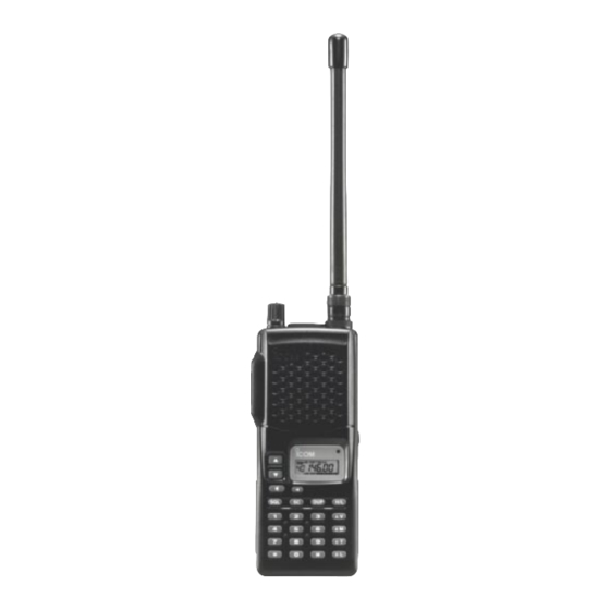
Icom IC-T2H Service Manual
144 mhz fm transceiver
Hide thumbs
Also See for IC-T2H:
- Instruction manual (50 pages) ,
- Instruction manual (45 pages) ,
- Instruction manual (48 pages)
Table of Contents
Advertisement
Advertisement
Table of Contents

Subscribe to Our Youtube Channel
Related Manuals for Icom IC-T2H


Summary of Contents for Icom IC-T2H
- Page 1 144 MHz FM TRANSCEIVER iC-t2h iC-t2e-t...
- Page 2 INTRODUCTION This service manual describes the latest service information for the IC-T2H/E-T FM TRANSCEIVER at the time of publication. MODEL VERSION SYMBOL U.S.A. Europe U.K. IC-T2H Italy Asia C.S. America/-1 CSA/-1 Taiwan Asia-1 IC-T2E-T Thailand To upgrade quality, all electrical or mechanical parts and inter- nal circuits are subject to change without notice or obligation.
-
Page 3: Table Of Contents
TABLE OF CONTENTS SECTION 1 SPECIFICATIONS SECTION 2 INSIDE VIEWS SECTION 3 DISASSEMBLY INSTRUCTIONS SECTION 4 CIRCUIT DESCRIPTION 4 - 1 RECEIVER CIRCUITS ....................4 – 1 4 - 2 TRANSMITTER CIRCUITS ................... 4 – 2 4 - 3 PLL CIRCUIT ........................4 – 3 4 - 4 POWER SUPPLY CIRCUITS .................. - Page 4 SECTION 1 SPECIFICATIONS GENERAL • Frequency coverage Version Transmit Receive U.S.A. 140.000–150.000 MHz* 136.000–174.000 MHz* Europe, U.K. 144.000–146.000 MHz 144.000–146.000 MHz Thailand Italy, Asia, 136.000–174.000 MHz* 136.000–174.000 MHz* ANI, C.S.A. Taiwan 145.000–146.000 MHz 145.000–146.000 MHz Guaranteed frequency range: 144–148 MHz •...
- Page 5 SECTION 2 INSIDE VIEWS • MAIN UNIT TOP VIEW BOTTOM VIEW Low-pass filter circuit Antenna switching circuit (D8, D32: HVU131TRF) RF amplifier (Q12: 2SK360IG) Current detector circuit 1st mixer circuit (Q13: 2SK360IG) Crystal filter (FI1: FL-251 30.85 MHz) Power amplifier (Q1: 2SK3075) VCO circuit Analog switch*...
- Page 6 SECTION 3 DISASSEMBLY INSTRUCTIONS • Removing the chassis panel q Unscrew 1 nut, , and remove 1 nob, w Unscrew 2 screws, e Remove the the chassis in the direction of the arrow. r Unplug J6 to separate front panel and chassis. (nickel, 2 mm) ×...
-
Page 7: Circuit Description
SECTION 4 CIRCUIT DESCRIPTION 4-1 RECEIVER CIRCUITS The signals from the RF circuit are mixed at the 1st mixer (Q13) with a 1st LO signal coming from the VCO circuit to 4-1-1 ANTENNA SWITCHING CIRCUIT produce a 30.85 MHz 1st IF signal. Received signals passed through the low-pass filter (L1–L3, λ... -
Page 8: Transmitter Circuits
The AF signals from the [VOL] control are applied to the AF 4-2 TRANSMITTER CIRCUITS power amplifier circuit (IC5, pin 4) to obtain the specified 4-2-1 MICROPHONE AMPLIFIER CIRCUIT audio level. The amplified AF signals, output from pin 10, are The microphone amplifier circuit amplifies audio signals with applied to the internal speaker (SP1) via the [SP] jack when +6 dB/octave pre-emphasis characteristics from the micro-... -
Page 9: Pll Circuit
4-2-5 APC CIRCUIT A portion of the VCO signal is amplified at the buffer-amplifi- er (Q4, Q6) and is then applied to the receive 1st mixer or The APC circuit (IC3a, Q37) protects drive and power ampli- transmit buffer-amplifier circuit via the T/R switching diode fiers from excessive currents and selects HIGH or LOW out- (D3, D4). -
Page 10: Port Allocations
4-5 PORT ALLOCATIONS CPU (IC8) Port Port Description Description number name number name Input port for CTCSS signal for decod- Output ports for: ing. • tunable bandpass filter control 54–60 T4/PWR signal while receiving. RESET Input port for the reset signal. •... -
Page 11: Adjustment Procedures
SECTION 5 ADJUSTMENT PROCEDURES 5-1 PREPARATION REQUIRED TEST EQUIPMENT GRADE AND RANGE EQUIPMENT GRADE AND RANGE EQUIPMENT Output voltage : 9.6 V DC Frequency range : 300–3000 Hz Audio generator DC power supply Current capacity : 5 A or more Measuring range : 1–500 mV Measuring range... -
Page 12: Pll And Transmitter Adjustments
5-2 PLL AND TRANSMITTER ADJUSTMENTS ADJUSTMENT MEASUREMENT POINT ADJUSTMENT ADJUSTMENT CONDITION VALUE UNIT LOCATION UNIT ADJUST PLL LOCK • Operating frequency : 146.000 MHz MAIN Connect a digital multi- 1.40 V VOLTAGE • Receiving meter to the check board point LV. REFERENCE •... -
Page 13: Receiver Adjustment
5-3 RECEIVER ADJUSTMENT ADJUSTMENT MEASUREMENT POINT ADJUSTMENT ADJUSTMENT CONDITION VALUE UNIT LOCATION UNIT ADJUST SENSITIVITY • Operating freq. : 146.000 MHz MAIN Connect a digital volt- Maximum level MAIN Adjust in • Connect an SSG to the antenna con- meter to check point S. sequence nector and set as: L18, L19... - Page 14 SECTION 6 PARTS LIST [MAIN UNIT] [MAIN UNIT] ORDER ORDER DESCRIPTION DESCRIPTION 1130007610 S.IC µPD3140GS-E1 (DS8) 6050009420 XTAL CR-514 (15.200000 MHz) 1110003490 S.IC TA31136FN (D/EL) 6050010110 S.XTAL CR-584 (6.79966 MHz) 1110003780 S.IC NJM2902V-TE1 6050009020 S.CERAMIC EFOS4194E3 [ANI] only 1130008090 S.IC BU4066BCFV-E1 6070000210 S.DISCRIMINATOR CDBCA450CX24 1110001810 S.IC...
- Page 15 [MAIN UNIT] [MAIN UNIT] ORDER ORDER DESCRIPTION DESCRIPTION ERJ3GEYJ 331 V (330 Ω) 7030003480 S.RESISTOR ERJ3GEYJ 222 V (2.2 kΩ) R183 7030003380 S.RESISTOR ERJ3GEYJ 560 V (56 Ω) 7030003290 S.RESISTOR R186 7030003640 S.RESISTOR ERJ3GEYJ 473 V (47 kΩ) 7030003480 S.RESISTOR ERJ3GEYJ 222 V (2.2 kΩ) R191 7030003590 S.RESISTOR...
- Page 16 [MAIN UNIT] [MAIN UNIT] ORDER ORDER DESCRIPTION DESCRIPTION R295 7030003440 S.RESISTOR ERJ3GEYJ 102 V (1 kΩ) C118 4030006900 S.CERAMIC C1608 JB 1E 103K-T-A R296 7030003440 S.RESISTOR ERJ3GEYJ 102 V (1 kΩ) C119 4030008680 S.CERAMIC C2012 JF 1C 105Z-T-A R297 7030003440 S.RESISTOR ERJ3GEYJ 102 V (1 kΩ) C120 4030011600 S.CERAMIC...
-
Page 17: Vco Board
[MAIN UNIT] [VCO BOARD] ORDER ORDER DESCRIPTION DESCRIPTION C231 4030011600 S.CERAMIC C1608 JB 1C 104KT-N 1530002920 S.TRANSISTOR 2SC4226-T2 R25 C232 4030011600 S.CERAMIC C1608 JB 1C 104KT-N 1530002920 S.TRANSISTOR 2SC4226-T2 R25 C233 4030006860 S.CERAMIC C1608 JB 1H 102K-T-A 1530002920 S.TRANSISTOR 2SC4226-T2 R25 C234 4030006860 S.CERAMIC C1608 JB 1H 102K-T-A... -
Page 18: Cabinet Parts
SECTION 7 MECHANICAL PARTS AND DISASSEMBLY 7-1 CABINET PARTS [CHASSIS PARTS] [CHASSIS PARTS] ORDER ORDER REF NO. DESCRIPTION QTY. REF NO. DESCRIPTION QTY. 6510020350 ANT connector BNC-R148 MP23 8810009510 Screw PH BT M2×4 NI-ZU MP24 8810009560 Screw PH BT M2×6 ZK SP 1 2510000960 Speaker K036NA500-26 MP25... - Page 19 MP20 (C) J1 (C) MP10 (C) MP4 (C) MP26 (C) MP23 (C) MP18(C) MP22 (C) MP32 (C) MP11 (C) MP35 (C) VR board MP21 (C) MP1 (C) MP21 (C) MP7 (C) MP34 (C) MP33 (C) MP17 (C) MP1 (M) MP5 (C) MP31 (C) MP25 (C) MP30 (C)
- Page 20 SECTION SECTION 8 PARTS LIST SEMI-CONDUCTOR INFORMATION 8 - 1 TRANSISTORS 8 - 2 DIODES NAME SYMBOL INSIDE VIEW NAME SYMBOL INSIDE VIEW NAME SYMBOL INSIDE VIEW NAME SYMBOL INSIDE VIEW DA112 MA6S121 2SA1588 - GR 2SK880 - Y A2 A1 DTA114TU DA113W MA77...
- Page 21 SECTION 9 BOARD LAYOUTS The combination of this page and the next page shows 9 - 1 MAIN UNIT the unit layout in the same configuration as the actual P.C. Board. • TOP VIEW ANTENNA (CHASSIS) VCO OUT SHIFT SPG SP SPEAKER BATT VOL IN...
- Page 22 The combination of this page and the previous page shows the unit layout in the same configuration as the MAIN UNIT CHARGER actual P.C. Board. • BOTTOM VIEW (CHASSIS) EMIC VCOOUT EXT.MIC SHIFT AF OUT EXT.SP BOARD CLONE BATT VOL IN VOL OUT BOARD PTT SWITCH...
- Page 23 SECTION 10 BLOCK DIAGRAM 10 - 1...
- Page 24 SECTION 11 VOLTAGE DIAGRAM R289 9.5V CL IN K036NA500-26A27 CPU5 CPU5 C164 TEMP 0.001 2SA1588 5.0V R182 C256 TX: 5 NTCCF20124AH 473 k 0.001 RX: 0 R215 IC11 2SB1132 330 k C148 S-80742SL-A6 2SB1201 R220 C248 220 k 0.01 R181 C232 2SA1588 100 k...
- Page 25 R161 2SK880 0.15 5.0V R298 0.001 60 nH 60 nH 60 nH R186 LNJ310M6URA C234 47 k 0.001 C233 C256 TX: 5V 0.001 TX: 3.8V R160 2SC4081 R238 0.001 RX: 0V 4.5V R162 VCO BOARD R183 0.001 2.9V 56 nH CHASSIS LNJ310M6URA 0.001...
- Page 26 SECTION 11 VOLTAGE DIAGRAM R289 9.5V CL IN K036NA500-26A27 R161 2SK880 5.0V 0.15 R298 0.001 60 nH 60 nH 60 nH CPU5 CPU5 R186 LNJ310M6URA C234 C164 TEMP 47 k 0.001 C233 0.001 5.0V 2SA1588 R182 C256 TX: 5V 0.001 TX: 3.8V R160 NTCCF20124AH...
- Page 27 08190 Sant Cugat Del Valles Barcelona, SPAIN Phone : ( 93 ) 589 46 82 Fax : ( 93 ) 589 04 46 A Division of Icom America Inc. E-mail : icom@lleida.com 3071 #5 Road, Unit 9, Richmond, B.C., V6X 2T4, Canada...
- Page 28 Count on us! A-5518MI-S 6-9-16, Kamihigashi, Hirano-ku, Osaka 547-0002, Japan © 1998 by Icom Inc.
Need help?
Do you have a question about the IC-T2H and is the answer not in the manual?
Questions and answers