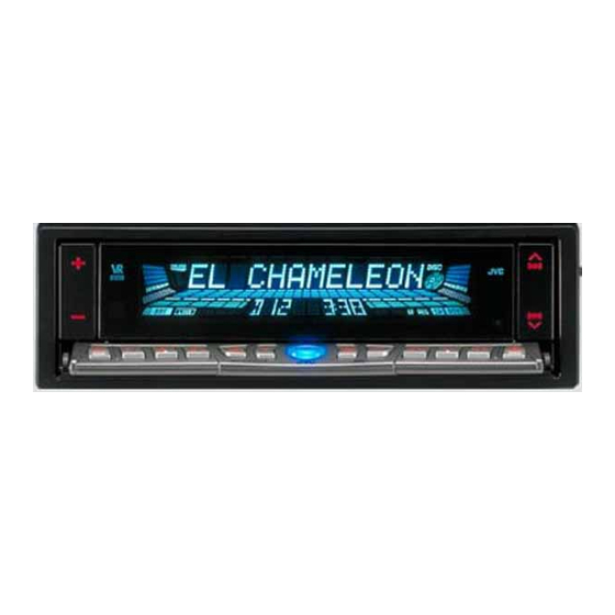
JVC KD-LX50R Service Manual
Cd receiver
Hide thumbs
Also See for KD-LX50R:
- Installation & connection manual (6 pages) ,
- Instructions manual (314 pages) ,
- Service manual (74 pages)
Table of Contents
Advertisement
Quick Links
KD-LX50R
VICTOR COMPANY OF JAPAN, LIMITED
MOBILE ELECTRONICS DIVISION
PERSONAL & MOBILE NETWORK B.U. 10-1,1Chome,Ohwatari-machi,Maebashi-city,Japan
(No.49562)
SERVICE MANUAL
Contents
Safety precaution
Preventing static electricity
Instructions
Disassembly method
Maintenance of laser pickup
Extention cord connectiong method 2-13
Functions of the mechanism under
the service mode
Printed in Japan
200005(O)
CD RECEIVER
KD-LX50R
VCR
/I
AT T
SCM
MONO
LOCAL
MODE
S
DISP
SOURCE
BBE
BAND
INT
RPT
RND
SEL
7
8
9
S
10
11
12
OFF
M
KD-LX50R
Flow of functional operation
1-2
until TOC read
1-3
Description of major ICs
1-4~
Block diagram
2-1
Standard schematic diagrams
2-12
Printed circuit boards
Parts list
2-16
This service manual is printed on 100% recycled paper.
COPYRIGHT
2000 VICTOR COMPANY OF JAPAN, LTD.
KD-LX50R
Area Suffix
E ---- Continental Europe
2-18
2-20
2-
2-
2-
3-1~19
No.49562
May. 2000
Advertisement
Table of Contents

Subscribe to Our Youtube Channel
Related Manuals for JVC KD-LX50R


Summary of Contents for JVC KD-LX50R
- Page 1 KD-LX50R KD-LX50R SERVICE MANUAL CD RECEIVER KD-LX50R Area Suffix E ---- Continental Europe AT T MONO LOCAL MODE DISP SOURCE BAND KD-LX50R Contents Flow of functional operation Safety precaution until TOC read 2-18 Preventing static electricity Description of major ICs...
-
Page 2: Preventing Static Electricity
Preventing static electricity 1.Grounding to prevent damage by static electricity Electrostatic discharge (ESD), which occurs when static electricity stored in the body, fabric, etc. is discharged, can destroy the laser diode in the traverse unit (optical pickup). Take care to prevent this when performing repairs. 2.About the earth processing for the destruction prevention by static electricity Static electricity in the work area can destroy the optical pickup (laser diode) in devices such as CD players. -
Page 3: Important For Laser Products
Important for laser products 5.CAUTION : If safety switches malfunction, the laser is able 1.CLASS 1 LASER PRODUCT to function. 2.DANGER : Invisible laser radiation when open and inter 6.CAUTION : Use of controls, adjustments or performance of lock failed or defeated. Avoid direct exposure to beam. procedures other than those specified herein may result in 3.CAUTION : There are no serviceable parts inside the hazardous radiation exposure. -
Page 4: Disassembly Method
Disassembly method Bottom cover Removing the top chassis (See Fig.1 to 5) Remove the two screws A attaching the bottom cover to the top chassis on the bottom of the body. Remove the two screws B attaching the top chassis on both sides of the body. - Page 5 Removing the main board assembly (See Fig.6 and 7) Prior to performing the following procedure, remove the top chassis. CN504 CN503 Disconnect the flexible harness from connector CN701 CN701, the card wire from CN702 on the main board harness from CN503 CN504 respectively.
-
Page 6: Removing The Front Panel Assembly
Removing the front panel assembly (See Fig.8,9 and 10) Prior to performing the following procedure, remove the top chassis assembly. CN701 Disconnect the flexible harness from connector CN701 on the main board assembly. Remove the four screws N attaching the front panel assembly on both sides of the body. - Page 7 Removing the lifter unit (See Fig.12) Prior to performing the following procedure, remove the top chassis assembly and the front panel assembly. Disconnect the harness from connector CN503 and CN504 CN503 CN504 on the main board. Remove the four screws P and detach the lifter unit from the bottom cover.
- Page 8 Removing the operation assembly (See Fig.15 to 18) Prior to performing the following procedure, remove the top chassis assembly, the front panel assembly and the lifer unit. Bracket (R) Remove the screws S attaching the right and left Bracket (L) brackets which fix gears on both sides of the operation assembly.
- Page 9 Removing the operation switch board (See Fig.19 and 20) Prior to performing the following procedure, remove the operation assembly. Remove the six screws T attaching the button panel on the operation assembly. Pull out the operation switch board from inside of the button panel.
- Page 10 Disassembly method <Voice unit> Top cover Removing the voice recorder (See Fig.1 to 3) Remove the two screws A on both sides of the body and detach the top cover upward. Remove the two screws B and the two screws C attaching the voice board.
- Page 11 Damper bracket Removing the CD mechanism control CD mechanism ass’y board(See Fig.1 and 2) Unsolder the part a and b on the CD mechanism control board. Remove the stator c fixing the CD mechanism control board and the damper bracket (To remove the stator smoothly, pick up the center part).
- Page 12 Removing the loading motor Loading motor (See Fig.3 to 5) Prior to performing the following procedure, remove the CD mechanism control board. Belt Remove the two springs f attaching the CD mechanism ass’y and the front bracket. Fig.5 Remove the two screws B and the front bracket while pulling the flame outward.
-
Page 13: Removing The Pickup Unit
Removing the feed motor ass’y Part j FD screw (See Fig.10) Feed motor ass’y Prior to performing the following procedure, remove the CD mechanism control board, the front bracket Part k (loading motor) and the CD mechanism ass’y. Remove the two screws F and the feed motor ass’y. Pickup unit FD gear Pickup unit... -
Page 14: Adjustment Method
Adjustment method Caution : Replacing the pickup To prevent damage to the laser diode Caution : static electricity destroys the laser diode. Solder rejection or cuts a pattern with nipper at shortstop point after short Always take countermeasure performing repairs around the laser circuiting with clip with terminal face of pickup. -
Page 15: Maintenance Of Laser Pickup
Maintenance of laser pickup (1) Cleaning the pick up lens Before you replace the pick up, please try to clean the lens with a alcohol soaked cotton swab. (2) Life of the laser diode When the life of the laser diode has expired, the following symptoms will appear. -
Page 16: Extension Cord Connecting Method
Extension cord connecting method Using the extention cords to connect the front panel with the main board Remove the main board follwing the disassembly methode. Then reattachi the heat sink to main board. Using the 2pin extention cord (EXTLX001-2p), Using the jig board (EXTLX002-SWPWB), its connect the harness of the feed motor (L) assembly installing to the chassis, then using 4pin extention with the connector CN503 on the main board. - Page 17 Extension cord list for KD-LX50R EXTLX002-JIG : Kit including the following 8 extension parts. Parts number Quantity Description EXTLX001-2P 2Pin, 30cm extension cord EXTLX001-6PF 6Pin, 30cm flat wire EXTLX001-6PC 6Pin x 2, interlocking connector EXTLX002-16PF 16Pin flat wire EXTLX002-16PC 16Pin, interlocking connector...
- Page 18 Reassembly 1. Perform reassembly be reversing the removing process of "removal of main parts". CAUTION 1: Prior to reattaching the heat sink, make sure to reattache the top chassis.
-
Page 19: Functions Of The Mechanism Under The Service Mode
Functions of the mechanism under the service mode With the three error modes stored in maximum in the internal memory of the mechanism in the body of this system, it is posible under the service mode to call the contents of error according to the following steps when any error has occurred. - Page 20 1. Display of mechanism error Occurrence condition Description Error codes 09 0011 1. SW4 is not turned off. Disc loading error 09 0013 2. SW3 is not turned on. Eject error 01 0021 1. SW# is not turned off. 1. In case SW2 has been positioned to "L" before 80 0031 Error during standby for loading starting loading during waiting for 15sec.
-
Page 21: Flow Of Functional Operation Until Toc Read
Flow of functional operation until TOC read Power ON • When the laser diode correctly Set Function to CD • When the pickup correctly moves emits to the inner area of the disc Microprocessor Microprocessor Disc inserted commands commands MN662748RPM 57 MN662748RPM "32"... -
Page 22: Feed Section
Feed Section Is the voltage output at Is the wiring for IC941 Is 5V present at IC601 Check CD 9V IC631 pin "26" 2.5V or (10) ~ (15) correct? pin "5"? and 5V. Check the vicinity of IC941. Is 4V present at both Is 6V or 2V present at Check the feed motor sides of the feed motor? - Page 23 BA3220FV-X (IC301,IC401) : Driver 1. Pin layout & Block diagram LGND OUTL OUTR RGND CR - CR + REFL REFR FILTER 2. Pin functions Symbol Function Powe supply terminal for amp. power supply terminal. input terminal. Negative feedback terminal. Filter terminal. Negative feedback terminal.
- Page 24 BA4905-V3 (IC961) : Regulator 1.Terminal layout 2.Block diagram REGULATOR RESET RESET COMP VDD 5.7V CD 8V AUDIO 9V CTRL ILM 10V 3.Pin function Pin no. Symbol Function RESET If VDD voltage becomes 4V or less.RESET output becomes low level. EXT output This output voltage is approximately 0.5V lower than VCC.
-
Page 25: Pin Layout
BD3860K (IC911) : E. volume 1. Pin layout 2. Block diagram GND FIL VCC SEL1 VIN1 LOUD1 HF1 LF1 DET1 VCA1 MIX1 BBOUT1 TIN1 TNF1 BNF1 BOUT1 POWER FADER SUPPLY MAIN INPUT CH1 FRONT OUTF1 TREBLE BASS VOLUME GAIN 0 to -5 dB LOW(f=50Hz) 6dB 0 to -40 dB -14 to +14dB... - Page 26 BR24C32F-X (IC703) : EEPROM 1. Pin function 2. Block diagram A0 1 8 Vcc 32k bit EEPROM ARRAY 8bit 12bit SLAVE/WORD ADDERESS DATA A1 2 7 WP 12bit ADDRESS REGISTER DECODER REGISTER START STOP A2 3 6 SCL CONTROL LOGIC GND 4 5 SDA HIGH VOLTAGE GEN.
- Page 27 BU4066BCFV-X (IC322) : Quad analog switch 1. Pin layout & Block diagram I/O4 O/I4 O/I3 I/O3 I/O1 O/I1 O/I2 I/O2...
- Page 28 FAN8037 (IC581) : CD driver 1. Pin layout & Block diagram 48 47 46 45 44 43 42 41 40 39 38 37 STAND BY T.S.D ALL MUTE POWER SAVE 13 14 15 16 17 18 19 20 21 22 23 24 2.
- Page 29 HD74HC126FP-X (IC801) : Buffer 1. Pin layout 2. Function Inputs Outputs 3. Block diagram Output Input Output Sample as Load Circuit 1 Output Sample as Load Circuit 1 Output Sample as Load Circuit 1...
- Page 30 IC-PST600M/G/-W (IC702) : System reset Vout...
- Page 31 LA3460M-X (IC31) : FM noise canceller & Stereo MPX demodulator 1. Pin layout 2. Block diagram DRIVER VCO STOP PACAN SCHMIT SEPARATION ADJ. ANTI-BRIDGE MAIN GATE DECODER TRIG CONTROL 3. Pin function Function Description Noise sense Noise sensitivity adjustment Noise AGC Gate time Signal hold Pilot output...
- Page 32 LA4743B (IC941) :Power amp 1.Terminal layout 2 3 4 5 6 7 8 9 10 11 12 13 14 15 16 17 18 19 20 21 22 23 24 25 2.Block diagram 3.Pin function No. Symbol Function No. Symbol Function Header of IC LFIN Front Lch input...
- Page 33 LC75811W (IC602) : LCD driver 1. Pin layout 2. Block diagram COMMON SEGMENT DRIVER DRIVER LATCH CGRAM CGROM ADRAM VLCD INSTRUCTION 5x9x16 5x9x240 DECODER bits bits bits VLCD1 VLCD2 ADDRESS DCRAM INSTRUCTION VLCD3 COUNTER 48x8 REGISTER bits ADDRESS REGISTER TIMING GENERATOR SHIFT REGISTER CLOCK...
- Page 34 LC75823W (IC601) : LCD driver 1. Pin Layout & Symbol 64 63 62 61 60 59 58 57 56 55 54 53 52 51 50 49 17 18 19 20 21 22 23 24 25 26 27 28 29 30 31 32 2.
- Page 35 M5282FP-XE (IC321) : E. volume 1. Pin layout 2. Block diagram 3. Pin function Symbol Function Vcc/2 Vcc/2 output for microphone amp. Amp+IN Microphone amp. positive input terminal. Amp-IN Microphone amp. negative input terminal. Amp OUT Microphone amp. output terminal. Ground.
- Page 36 MSM534001E-77TS (IC854) : Flash memory 1. Pin layout 2. Pin function Symbol Function A0~A18 Address input 16 15 14 13 12 11 10 9 D0~D7 Data output Chip enable Output enable Vcc,Vss Power supply Non connection 17 18 19 20 21 22 23 24 25 26 27 28 29 30 31 32 3.
- Page 37 NJM2100M-W (IC821) : Dual operation amplifier 1. Pin layout A OUTPUT A - INPUT B OUTPUT A + INPUT B - INPUT B + INPUT 2. Block diagram - INPUT OUTPUT + INPUT...
- Page 38 NJM2904M-W (IC831) : Ope amp 1.Pin layout A OUT A -IN B OUT A +IN B -IN B +IN 2.Block diagram OUTPUT...
- Page 39 NJM4565M-W (IC151,IC171,IC323) : Ope amp. A OUTPUT A -INPUT B OUTPUT A +INPUT B -INPUT B +INPUT...
- Page 40 RPM6938-V4 (IC602) : R.M. Receiver 22k ohm Comp Detector conversion fo trimming circuit Magnetic shield...
- Page 41 RSC-300-TQFP (IC851) : Voice processor 1. Pin layout 2. Block diagram PORT PORT PRE-AMP SPEECH INTERRUPT LOGIC PROCESSING UNIT EXTERNAL MEMORY INTERFACE 3. Pin function Symbol I/O Function Symbol Function Address bus for external memory Data enable siganl from 78K0 Address bus for external memory Dtat request signal for 78K0 Address bus for external memory...
- Page 42 S-81250SGUP-X (IC845) : Regulator 1. Pin layout 2. Block diagram VOUT 1 GND 2 VIN 3 VOUT Ref.
- Page 43 SAA6579T-X (IC51) : RDS demodulator 1. Pin layout 2. Pin function Symbol Function QUAL Quality indication output RDDA RDS data output Vref Reference voltage output (0.5VDDA) Multiplex signal input VDDA +5V supply voltage for analog part VSSA Ground for analog part (0V) Sub carrier input to comparator SCOUT Sub carrier output of reconstruction filter...
- Page 44 SST28SF040120IE (IC853) : EEPROM 1. Pin layout 2. Block diagram 4,194,304Bit EEPROM X-Decoder Cell Array A18~A0 Address Buffer & Latches Y-Decoder Control Logic I/O Buffers & Data Latches DQ7~DQ0 3. Pin function Symbol Pin name Function A18~A8 Row Address Inputs To provide memory address.
-
Page 45: Block Diagram
TA2109F-X (IC501) : RF amp. 1. Pin layout 2. Block diagram 15k ohm 30k ohm 7.67k ohm 15k ohm 10k ohm SBAD 10k ohm 20uA 50k ohm 30k ohm 20pF 10k ohm 10k ohm 36pF 21k ohm 29k ohm 2VRO 7.96k ohm 10k ohm 24k ohm 24k ohm... - Page 46 TC74VHCT08AF-X (IC856) : Buffer 1. Pin layout 2.Trouth table 1A 1 14 Vcc 1B 2 13 4B 1Y 3 12 4A 2A 4 11 4Y 2B 5 10 3B 2Y 6 GND 7...
- Page 47 TC74VHCT32AF-X (IC857) : Buffer 1. Pin layout 2.Trouth table 1A 1 14 Vcc 1B 2 13 4B 1Y 3 12 4A 2A 4 11 4Y 2B 5 10 3B 2Y 6 GND 7...
- Page 48 TC9462F (IC541) : DSP & DAC 1.Pin Layout 2.Pin Function (1/2) Symbol Function Pin No. Test mode terminal. Normally, keep at open TEST0 Playback speed mode flag output terminal Playback speed mode flag output terminal UHSO Sub code Q data emphasis flag output terminal. "H"=ON "L"=OFF EMPH Channel clock output terminal.(44.1kHz) "H"=Rch "L"=Lch LRCK...
- Page 49 2.Pin Function (2/2) Symbol Pin No. Function RFRP signal center level input terminal RFCT RFRP zero cross input terminal RFZI RF ripple signal input terminal RFRP Focus error signal input terminal Sub-beam adder signal input terminal SBAD Test input terminal Normally, keep at "vref" level TSIN Tracking error signal input terminal.
- Page 50 UPD784215GC-168 (IC701) : CPU 1. Pin layout 2. Pin function (1/2) Symbol Function CD mechanism detect switch CD mechanism detect switch CD mechanism detect switch REST-SW Reset signal input terminal from CD mechanism Loading motor control signal input terminal Loading motor control signal input terminal DIMMER-OUT DIMMER signal output terminal LCD-PWR...
- Page 51 2. Pin function (2/2) Pin No. Symbol Function LCD-DA Data output terminal for LCD driver LCD-CL Clock output terminal for LCD driver LCD-CE1 Chip enable 1 output terminal for LCD driver BUZZER BUZZER control signal output terminal E2PR-DA-I Data input terminal from EEPROM E2PR-DA-O Data output terminal for EEPROM E2PR-CLK...
- Page 52 UPD789104AMC504 (IC855) : Voice control CPU 1. Pin layout 2. Block diagram 8-bit TIMER/ PORT0 EVENT COUNTER 80 PORT1 16-bit TIMER 20 78K/0S PORT2 CORE WATCHDOG TIMER PORT5 SERIAL PORT6 INTERFACE SYSTEM CONTROL A/D CONVERTER INTERRUPT CONTROL 3. Pin function Symbol Function BUS-INT...
- Page 53 Line out PLLDA LEVEL IC51 FRONTL,FRONTR FRONT PLLCL VOL-DA Line out VOL-CLK RDSDA REARL,REARR REAR RDSSCK IC703 IC771 IC821 AMAF JVC BUS CRUISE EPROM SI/SO IC701 SI/SO,SO,I/OBUSINT,BUSSCK CRUISE AU.L,AU.R RESET LCDDA AU.LI,AU.RI IC171 Line IN W.VOL IC321 RESET LCDCL LINE IN...
-
Page 54: Standard Schematic Diagrams
Standard schematic diagrams Tuner & Main circuit section C163 D161 R162 1SS355 0.047 IC941 LA4743B QAU0157-001 C161 Q161 2SD601A 1/50 R165 R303 IC301 BA3220FV C307 100/10 C305 4.7/25 C308 4.7/25 R301 C301 C309 4.7/25 C120 47/16 4.7/25 C141 UN2211 C303 1/50 C310 470P... - Page 55 LCD & CD servo control section R252 C253 R255 1.5K R251 CD.R C251 4.7/25 R253 TRAY+ R-CH 120P TRAY- IC581 CN501 FAN8037 QGB2027M2-26X DOOR+ DOOR- TRACKING+ FOCUS+ FOCUS- R595 CDON R589 CDON 3.3K C153 R151 C151 4.7/25 R153 C156 100/10 L-CH LOADING- C584...
- Page 56 Voice control section R1018 R853 R1017 IC853 4.7k SST28SF040120IE R1016 C859 R1015 R1014 100/16 R1013 C855 C865 R1012 0.068 J851 R1011 QNS0076-001 FAD1 WRD2 FAD1 FAD0 FAD2 FAD0 J852 QNS0076-002 IC851 RSC-300-TQFP 0.022 C857 C856 C898 0.0056 100/10 FAD2 R852 C892 C891 R894...
- Page 57 Exploded view of general assembly and parts list Block No. 39 55...
- Page 58 Parts list (General assembly) Block No. M1MM Item Parts number Parts name Q'ty Description Area ------------ CD MECHA LV41606-001A FFC P.MECHA LV10189-001A-N CHASSIS TOP LV10188-001A FRONT COVER LV40828-002A BLIND LV31602-003A SIDE HEAT SINK LV31603-001A INSULATOR QYSPST2004M SCREW QYSDST2604Z SCREW T. CHAS+CD MECH QYSDSF2610Z TAPPING SCREW T.
- Page 59 Parts list (General assembly) Block No. M1MM Item Parts number Parts name Q'ty Description Area WDM214540 WASHER FOR CLUTCH ASS' QYSPSPU1725M SCREW LO.UNIT A+DIS.P LV30981-004A *CLUTCH ASS'Y LV10317-006A BUTTON PANEL LV10318-001A BUTTON BASE LV20615-002A PRESET BUTTON 1 LV20616-002A PRESET BUTTON 2 LV31613-001A FUNCTION BUTTON LV41825-001A...
- Page 60 Voice unit assembly and parts list Block No. Voice board Voice board (General assembly) Voice unit Parts list Block No. M2MM Item Parts number Parts name Q'ty Description Area LV31826-001A TOP COVER LV31827-001A BOTTOM CASE LV41143-001A SHEET LV41624-001A HOLE BASE QAM0249-002 DIN CORD CABLE QYSDST2606Z...
-
Page 61: Cd Mechanism Assembly And Parts List
CD mechanism assembly and parts list Block No. Grease G-31SA TN-CCD1001Z-138 G-31SA(Bottom side) RX-405 106 29... - Page 62 Parts list (CD mechanism) Block No. M3MM Item Parts number Parts name Q'ty Description Area 30310101T FRAME 30310103T DANPER PIN 30310107T UPPER PLATE 30310108T SEL STOP PLATE 30310142T SEL ARM (L)L 30310143T SEL ARM (R)L 30310145T S ARM SPRING(L) 30310112T TRIG LEVER 30310155T TRIG PL(Z)
- Page 63 Parts list (CD mechanism) Block No. M3MM Item Parts number Parts name Q'ty Description Area 19501403T WIRE CLAMPER 30311037T PICK UP FPC(Z) 30311036T CONNECT.PCB(Z-J 30311038T WIRE (5P-Z) 30311039T WIRE (LD-Z) 30311040T WIRE (FD-Z) 30311041T WIRE (RS-Z) 64180402T DET SWITCH ESE22MH1 64180403T DET SWITCH ESE22MH3...
- Page 64 Block No. 01 Electrical parts list (Main board) Item Remarks Parts number Parts name Area Item Parts number Parts name Remarks Area NCB21EK-473X C CAPACITOR C 202 NCS21HJ-681X C CAPACITOR QEKJ1CM-226Z E CAPACITOR 22MF 20% 16V C 203 QEKJ1HM-224Z E CAPACITOR .22MF 20% 50V NCB21HK-103X C CAPACITOR...
- Page 65 Block No. 01 Electrical parts list (Main board) Item Remarks Parts number Parts name Area Item Parts number Parts name Remarks Area C 458 NCB21CK-224X C CAPACITOR C 724 NCB21HK-222X C CAPACITOR C 459 NCB21CK-224X C CAPACITOR C 754 NCB21EK-104X C CAPACITOR C 501 QERF0JM-107Z...
- Page 66 Block No. 01 Electrical parts list (Main board) Item Remarks Parts number Parts name Area Item Parts number Parts name Remarks Area D 11 MA152WK-X SI DIODE Q 35 2SB709A/R/-X TRANSISTOR D 31 1SS355-X DIODE Q 36 UN2211-X TRANSISTOR D 101 MA152WK-X SI DIODE Q 131...
- Page 67 Block No. 01 Electrical parts list (Main board) Item Remarks Item Parts number Parts name Remarks Area Parts number Parts name Area R 54 NRSA02J-222X MG RESISTOR R 304 NRSA02J-333X MG RESISTOR R 101 NRSA02J-103X MG RESISTOR R 305 NRSA02J-154X MG RESISTOR R 102 NRSA02J-223X...
- Page 68 Block No. 01 Electrical parts list (Main board) Item Remarks Item Parts number Parts name Remarks Area Parts number Parts name Area R 536 NRSA02J-333X MG RESISTOR R 743 NRSA02J-473X MG RESISTOR R 537 NRSA02J-103X MG RESISTOR R 746 NRSA02J-473X MG RESISTOR R 541 NRSA02J-122X...
- Page 69 Electrical parts list Block No. 01 (Main board) Item Remarks Parts number Parts name Area R 987 NRSA02J-473X MG RESISTOR S 651 NSW0120-002X PUSH SWITCH S 652 NSW0120-002X PUSH SWITCH S 653 NSW0120-002X PUSH SWITCH TH951 NAD0021-103X THERMISTOR TH981 NAD0021-103X THERMISTOR TU 1 QAU0157-001...
- Page 70 Block No. 02 Electrical parts list (LCD&Switch Board) Item Remarks Parts number Parts name Area Item Parts number Parts name Remarks Area C 601 NBE20JM-475X TS E CAPACITOR R 635 NRSA02J-221X MG RESISTOR C 602 NCB21HK-104X C CAPACITOR R 636 NRSA02J-821X MG RESISTOR C 603...
- Page 71 Block No. 03 Electrical parts list (Boice board) Item Remarks Parts number Parts name Area Item Parts number Parts name Remarks Area C 841 QETM1CM-228 E CAPACITOR 2200MF 20% 16V J 853 QNZ0111-001 JACK C 842 NCB21HK-103X C CAPACITOR L 841 QQR0905-001 CHOKE COIL C 843...
- Page 72 Electrical parts list Block No. 03 (Voice board) Item Remarks Parts number Parts name Area R1014 NRSA02J-473X MG RESISTOR R1015 NRSA02J-473X MG RESISTOR R1016 NRSA02J-473X MG RESISTOR R1017 NRSA02J-473X MG RESISTOR R1018 NRSA02J-473X MG RESISTOR R1019 NRSA02J-103X MG RESISTOR R1020 NRSA02J-472X MG RESISTOR R1022...
-
Page 73: Packing Materials And Accessories Parts List
Packing materials and accessories parts list Block No. Block No. A1~A3 A9~A13 A14,A15 A4~A8 A18,A20 A17,A19... -
Page 74: Packing Parts List
Packing parts list Block No. M4MM Item Parts number Parts name Q'ty Description Area QPA01703505P POLY BAG INST BOOK QPA00801205 POLY BAG INST BOOK QPC03004315P POLY BAG LV31735-001A CARTON LV10193-201A PAPER CUSHION LV20660-001A CARTON BOX FOR VOICE UNIT Accessories parts list Block No.
Need help?
Do you have a question about the KD-LX50R and is the answer not in the manual?
Questions and answers