Table of Contents
Advertisement
Quick Links
Download this manual
See also:
Instruction Manual
QQ
3 7 63 1515 0
SERVICE MANUAL
4
2003
49793
TE
L 13942296513
1
Precautions . . . . . . . . . . . . . . . . . . . . . . . . . . . . . . . . . . . . . . . . . . . . . . . . . . . . . . . . . . . . . . . . . . . . . . . . . . . . 3
2
Disassembly method . . . . . . . . . . . . . . . . . . . . . . . . . . . . . . . . . . . . . . . . . . . . . . . . . . . . . . . . . . . . . . . . . . . . 5
3
Adjustment. . . . . . . . . . . . . . . . . . . . . . . . . . . . . . . . . . . . . . . . . . . . . . . . . . . . . . . . . . . . . . . . . . . . . . . . . . . . 28
4
Description of major ICs . . . . . . . . . . . . . . . . . . . . . . . . . . . . . . . . . . . . . . . . . . . . . . . . . . . . . . . . . . . . . . . . . 32
www
.
http://www.xiaoyu163.com
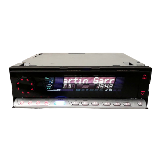
CD RECEIVER
KD-LX555R
S
S
TABLE OF CONTENTS
x
ao
u163
y
i
COPYRIGHT © 2003 VICTOR COMPANY OF JAPAN, LTD.
http://www.xiaoyu163.com
2 9
8
Q Q
3
6 7
1 3
1 5
KD-LX555R
7
8
9
T
D
M
SOURCE
co
.
9 4
2 8
0 5
8
2 9
9 4
12
Area Suffix
E ------ Continental Europe
m
9 9
2 8
9 9
No.49793
2003/5
Advertisement
Chapters
Table of Contents

Subscribe to Our Youtube Channel
Related Manuals for JVC KD-LX555R


Summary of Contents for JVC KD-LX555R
- Page 1 3 7 63 1515 0 SERVICE MANUAL CD RECEIVER 49793 2003 KD-LX555R L 13942296513 KD-LX555R SOURCE Area Suffix E ------ Continental Europe TABLE OF CONTENTS Precautions ................3 Disassembly method .
- Page 2 http://www.xiaoyu163.com 3 7 63 1515 0 SPECIFICATION AUDIO AMPLIFIER SECTION Maximum Power Output Front 50 W per channel Rear 50 W per channel 19 W per channel into 4 Ω, 40 Hz to 20 000 Hz Continuous Power Output (RMS) Front at no more than 0.8% total harmonic distortion.
-
Page 3: Precautions
http://www.xiaoyu163.com SECTION 1 3 7 63 1515 0 Precautions Safety Precautions Burrs formed during molding may be left over on some parts of the chassis. Therefore, pay attention to such burrs in the case of preforming repair of this system. Please use enough caution not to see the beam directly or touch it in case of an adjustment or operation check. - Page 4 http://www.xiaoyu163.com Preventing static electricity 3 7 63 1515 0 Electrostatic discharge (ESD), which occurs when static electricity stored in the body, fabric, etc. is discharged, can destroy the laser diode in the traverse unit (optical pickup). Take care to prevent this when performing repairs. 1.2.1 Grounding to prevent damage by static electricity Static electricity in the work area can destroy the optical pickup (laser diode) in devices such as CD players.
-
Page 5: Disassembly Method
http://www.xiaoyu163.com SECTION 2 3 7 63 1515 0 Disassembly method Main body Heat sink 2.1.1 Removing the top chassis Top chassis (See Fig.1~5) (1) Remove the two screws A attaching the bottom cover to the top chassis on the bottom of the body. (2) Remove the two screws B attaching the top chassis on both sides of the body. - Page 6 http://www.xiaoyu163.com 2.1.2 Removing the front panel assembly 3 7 63 1515 0 (See Fig.6~8) • Prior to performing the following procedure, remove the top chassis assembly. (1) Disconnect the flexible harness from connector CN701 on the main board assembly. (2) Remove the four screws H attaching the front panel as- sembly on both sides of the body.
-
Page 7: See Fig.
http://www.xiaoyu163.com 2.1.3 Removing the Front Board 3 7 63 1515 0 Joints a (See Fig.9) • Prior to performing the following procedure, remove the top chassis assembly and the front panel assembly. (1) Remove the four screws I attaching the front board on the back of the front panel assembly and release the eight joints a. -
Page 8: See Fig.
http://www.xiaoyu163.com 2.1.5 Removing the feed motor (L) 3 7 63 1515 0 Lifter unit assembly (See Fig.11) • Prior to performing the following procedure, remove the lifter unit. (1) Remove the washer attaching the clutch assembly and de- tach the clutch assembly from the shaft of the lifter unit. (2) Remove the two screws K attaching the feed motor (L). -
Page 9: See Fig.
http://www.xiaoyu163.com 2.1.7 Removing the operation assembly 3 7 63 1515 0 (See Fig.13~16) Operation assembly • Prior to performing the following procedure, remove the top chassis assembly, the front panel assembly and the lifer unit. (1) Disconnect the card wire from connector CN702 on the main board and remove the operation assembly. - Page 10 http://www.xiaoyu163.com 2.1.8 Removing the operation switch board 3 7 63 1515 0 (See Fig.17~19) • Prior to performing the following procedure, remove the oper- ation assembly. (1) Remove the six screws N attaching the button panel on the operation assembly. (2) Release the bottom panel from the bottom base at the bot- tom of the operation switch assembly five joint c and re- move the bottom panel.
-
Page 11: Http://Www.xiaoyu163.Com
http://www.xiaoyu163.com 2.1.9 Removing the MP3 board assembly 3 7 63 1515 0 (See Fig.20,21) • Prior to performing the following procedure, remove the top chassis. Caution: Connector board Before disconnecting the card wire from connector CN601 on the MP3 board, solder the short-circuit point on the connector board in the CD mechanism assembly (Refer to Fig.20). - Page 12 http://www.xiaoyu163.com 2.1.11 Removing the main board assembly 3 7 63 1515 0 (See Fig.23~25) • Prior to performing the following procedure, remove the top chassis. CN831 CN830 (1) Disconnect the flexible harness from connector CN701, the card wire from CN702 on the main board and the harness from CN830 and CN831 respectively.
- Page 13 http://www.xiaoyu163.com 2.2 CD Mechanism section 3 7 63 1515 0 2.2.1 Removing the top cover (See Figs.1 and 2) (1) Remove the four screws A on the both side of the body. (2) Lift the front side of the top cover and move the top cover backward to release the two joints a.
- Page 14 http://www.xiaoyu163.com 2.2.2 Removing the connector board 3 7 63 1515 0 Wires (See Figs.3 to 5) CAUTION: Before disconnecting the flexible wire from the pickup, solder the short-circuit point on the pickup. No observance of this in- struction may cause damage of the pickup. (1) Remove the screw B fixing the connector board.
- Page 15 http://www.xiaoyu163.com 2.2.3 Removing the DET switch 3 7 63 1515 0 (See Figs.6 and 7) (1) Extend the two tabs c of the feed sw. holder and pull out the switch. (2) Unsolder the DET switch wire if necessary. switch Connector board Pickup...
- Page 16 http://www.xiaoyu163.com 2.2.4 Removing the chassis unit 3 7 63 1515 0 (See Figs.8 and 9) • Prior to performing the following procedure, remove the top Chassis unit cover and connector board. Suspension spring (L) Suspension spring (R) (1) Remove the two suspension springs (L) and (R) attaching the chassis unit to the frame.
- Page 17 http://www.xiaoyu163.com 2.2.5 Removing the clamper assembly 3 7 63 1515 0 (See Figs.10 and 11) • Prior to performing the following procedure, remove the top cover. (1) Remove the clamper arm spring. Clamper arm (2) Move the clamper assembly in the direction of the arrow to spring release the two joints d.
- Page 18 http://www.xiaoyu163.com 2.2.6 Removing the loading / feed motor assembly 3 7 63 1515 0 (See Figs.12 and 13) • Prior to performing the following procedure, remove the top cover, connector board and chassis unit. (1) Remove the screw C and move the loading / feed motor as- sembly in the direction of the arrow to remove it from the chassis rivet assembly.
- Page 19 http://www.xiaoyu163.com 2.2.7 Removing the pickup unit 3 7 63 1515 0 Pickup unit (See Figs.14 to 18) • Prior to performing the following procedure, remove the top cover, connector board and chassis unit. (1) Remove the screw D and pull out the pu. shaft holder from the pu.
- Page 20 http://www.xiaoyu163.com 2.2.9 Removing the trigger arm 3 7 63 1515 0 Joint k (See Figs.19 and 20) • Prior to performing the following procedure, remove the top cover, connector board and clamper unit. (1) Turn the trigger arm in the direction of the arrow to release Trigger arm the joint k and pull out upward.
- Page 21 http://www.xiaoyu163.com 2.2.11 Removing the mode sw. / select lock arm 3 7 63 1515 0 Link plate Joint t (See Figs.22 and 23) Mode sw. • Prior to performing the following procedure, remove the top plate assembly. Select lock arm (1) Bring up the mode sw.
- Page 22 http://www.xiaoyu163.com 2.2.12 Reassembling the mode sw. / select lock arm 3 7 63 1515 0 Select lock arm spring (See Figs.24 to 26) REFERENCE: Hook w Reverse the above removing procedure. Joint v (1) Reattach the select lock arm spring to the top plate and set Joint v the shorter end of the select lock arm spring to the hook w on the top plate.
- Page 23 http://www.xiaoyu163.com 2.2.13 Removing the select arm R / link plate 3 7 63 1515 0 Joint c' Link plate Joint r (See Figs.27 and 28) Select arm R Joint b' • Prior to performing the following procedure, remove the top plate assembly.
- Page 24 http://www.xiaoyu163.com 2.2.15 Removing the loading roller assembly 3 7 63 1515 0 (See Figs.31 to 33) Loading roller assembly • Prior to performing the following procedure, remove the Roller guide clamper assembly and top plate assembly. spring (1) Push inward the loading roller assembly on the gear side and detach it upward from the slot of the joint g' of the lock arm rivet assembly.
- Page 25 http://www.xiaoyu163.com 2.2.16 Removing the loading gear 5, 6 and 7 3 7 63 1515 0 Loading gear bracket (See Figs.35 and 36) • Prior to performing the following procedure, remove the top Loading gear 6 cover, chassis unit, pickup unit and top plate assembly. (1) Remove the screw K attaching the loading gear bracket.
- Page 26 http://www.xiaoyu163.com 2.2.17 Removing the gears 3 7 63 1515 0 Joint p' (See Figs.37 to 40) • Prior to performing the following procedure, remove the top Change plate cover, chassis unit, top plate assembly and pickup unit. rivet assembly • Pull out the loading gear 3. (See Fig.35.) (1) Pull out the feed gear.
- Page 27 http://www.xiaoyu163.com 2.2.18 Removing the turn table / spindle motor 3 7 63 1515 0 Turn table (See Figs.41 and 42) • Prior to performing the following procedure, remove the top cover, connector board, chassis unit and clamper assembly. (1) Remove the two screws L attaching the spindle motor as- sembly through the slot of the turn table on top of the body.
-
Page 28: Adjustment
Frequency Band (6) Digital tester 87.5MHz to 108.0MHz (7) Tracking offset meter AM (MW) 522kHz to 1620kHz (8) Test Disc JVC :CTS-1000 AM (LW) 144kHz to 279kHz (9) Extension cable for check EXTSH002-22P × 1 Dummy load Standard volume position Exclusive dummy load should be used for AM,and FM. - Page 29 http://www.xiaoyu163.com Flow of functional operation unit TOC read 3 7 63 1515 0 Power ON When the laser diode correctly Set Function CD When the pickup correctly moves emits to the inner area of the disc Microprocessor $82 $81 Disc inserted Microprocessor commands commands...
- Page 30 http://www.xiaoyu163.com Troubleshooting 3 7 63 1515 0 Feed section Is the voltage output at Is the wiring for IC681 Is 3.3V present at IC681 IC621 pin "40" 5V or 0V? pin 27? pin "20"? Check CD 8V Check the vicinity of and 5V.
- Page 31 http://www.xiaoyu163.com Maintenance of laser pickup 3 7 63 1515 0 3.10 Replacement of laser pickup (1) Cleaning the pick up lens Before you replace the pick up, please try to clean the lens Turn off the power switch and,disconnect the power cord from the ac outlet.
-
Page 32: Description Of Major Ics
http://www.xiaoyu163.com SECTION 4 3 7 63 1515 0 Description of major ICs BA6956AN (IC830, IC831) : Reversible motor driver • Block diagram CONTROL LOGIC • Pin function • Truth table Pin No. Symbol Function OUT1 OUT2 MODE VREF Output high voltage level control terminal Forward rotation mode OUT2 Output terminal for motor... - Page 33 http://www.xiaoyu163.com BR24C01AFV-W-X (IC1502) : EEPROM 3 7 63 1515 0 • Pin layout • Block diagram 1kbit EEPROM ARRAY 8bit 7bit ADDRESS SLAVE/WORD DATA 7bit DECODER ADDRESS REGISTER REGISTER START STOP CONTROL LOGIC L 13942296513 HIGH VOLTAGE GEN. Vcc LEVEL DETECT •...
- Page 34 http://www.xiaoyu163.com BR24C32F (IC703) : EEPROM 3 7 63 1515 0 • Pin Layout • Pin layout & Block diagram PIN NAME Function Power Supply Ground (0V) A0-A2 Slave Address Set BR24C32/F Serial Clock Input I/O Slave and Word Address. Serial Data Input$ Serial Data Output *1 Write Protect Input •...
- Page 35 http://www.xiaoyu163.com BU1923F (IC51) : RDS decoder 3 7 63 1515 0 • Pin layout QUAL RCLK RDATA N.C. Vref VDD1 VDD2 VSS1 VSS2 VSS3 • Block diagram VSS3 100k 120k 100k 8th Switched capacitor filter Vref comparator anti-aliasing filter VDD1 RCLK Analog Power supply...
- Page 36 http://www.xiaoyu163.com HA13164A (IC961) : Regulator 3 7 63 1515 0 • Terminal layout 1 2 3 4 5 6 7 8 9 10 11 12 13 14 15 • Block diagram 100u 0.1u BATT.DET OUT ANT OUT Surge Protector 0.1u EXT OUT COMPOUT BIAS...
- Page 37 http://www.xiaoyu163.com 4.7 HD74HCT126T-X : (IC1500,IC1503) Buffer 3 7 63 1515 0 • Pin arrangement • Pin function Input Output H : High level L : Low level X : Irrelevant Z : Off (Hhigh-impedance)state of a 3-stage output • Block diagram L 13942296513 u163 (No.49793)1-37...
- Page 38 http://www.xiaoyu163.com LA47505 (IC941) : Power amp. 3 7 63 1515 0 • Terminal layout Protective circuit Stand by Switch L 13942296513 Ripple Mute Filter circuit protective circuit Muting & On Time Control Circuit u163 1-38 (No.49793) http://www.xiaoyu163.com...
- Page 39 http://www.xiaoyu163.com • Terminal layout 3 7 63 1515 0 • Pin function Pin No. Symbol Function AC CONT1 Header of IC GND1 Power GND OUTFR- Outpur(-) for front Rch STBY Stand by input OUTFR+ Output (+) for front Rch Vcc1/2 Power input OUTRR- Output (-) for rear Rch...
- Page 40 http://www.xiaoyu163.com LA6579H-X (IC1681) : 4-Channel bridge driver 3 7 63 1515 0 • Pin layout & Block diagram VIN1-A VIN1 VIN1_SW [H]: OP-AMP_A [L]: OP-AMP_B VIN1+A VIN1-B VCCP1 VIN1+B Signal system S-GND power supply VIN1-SW All outputs ON/OFF H : ON VO2+ MUTE MUTE...
- Page 41 http://www.xiaoyu163.com • Pin function 3 7 63 1515 0 Pin No. Symbol Function VIN1-A CH1 input AMP_inverted input VIN1+A CH1 input AMP_non-inverted input VCCP1 CH1 and CH2 power stage power supply VO1+ Output pin(+)for channel 1 VO1- CH1 output pin (-) for channel 1 VO2+ Output pin(+)for channel 2 VO2-...
- Page 42 http://www.xiaoyu163.com 4.10 M61508FP (IC400) : E.volume 3 7 63 1515 0 • Pin layout & Block diagram VDD OUT 2 18 VDD OUT 1 CLOCK DATA SOFT TIMER SELECT DETECTOR NonFadaer OUT 2 NonFadaer OUT 1 NON FADER NON FADER VOLUME VOLUME FRONT OUT 2...
- Page 43 http://www.xiaoyu163.com • Pin function 3 7 63 1515 0 Pin No. Symbol Function IC signal GND DEFP IN 1 Ope amp positive input DEFN IN 1 Ope amp negative input INA 1 Input selector ch1 input terminal INB 1 Input selector ch1 input terminal INC 1 Input selector ch1 input terminal IND 1...
- Page 44 http://www.xiaoyu163.com 4.11 LC75878W (IC601) : LCD driver 3 7 63 1515 0 • Pin layout 100 ~ 76 26 ~ 50 • Block diagram COMMON GENERAL SEGMENT DRIVER & LATCH PORT DRIVER CLOCK CONTROL REGISTER GENERATOR VLCD CONTRAST SHIFT REGISTER ADJUSTER VLCD0 L 13942296513...
- Page 45 http://www.xiaoyu163.com 4.12 NJM4565V-X (IC1572) : Dual ope amp 3 7 63 1515 0 • Terminal layout & Pin function AOUTPUT A-INPUT A+INPUT B+INPUT B-INPUT B OUTPUT 4.13 NJU7241F25 (IC1651) : Regulator • Pin Layout • Block Diagram Short protect GND 1 5 STB VIN 2 3 VOUT...
- Page 46 http://www.xiaoyu163.com 4.15 TA2157FN-X (IC1601):RF amp 3 7 63 1515 0 • Terminal layout • Block diagram PEAK 50 A BOTTOM PEAK L 13942296513 1.75k 240k 15pF x0.5 240k 15pF x0.5 180k 40pF RFGC (APC SW) (TE BAL) (AGC Gian) (TE BAL) VCTRLPIN Normal mode APC ON...
- Page 47 http://www.xiaoyu163.com • Pin function 3 7 63 1515 0 Pin No. Symbol Function 3.3V power supply pin Main-beam amp input pin Main-beam amp input pin Sub-beam amp input pin Sub-beam amp input pin Monitor photo diode amp input pin Laser diode amp output pin APC circuit ON/OFF control signal, laser diode (LDO) control signal input or bottom/peak detection frequency change pin.
- Page 48 http://www.xiaoyu163.com 4.16 TC94A14FA (IC1621) : DSP & DAC 3 7 63 1515 0 • Terminal layout & block daiagram Clock generator 1-bit Servo control Digital equalizer Address automatic circuit adjustment circuit Data CLV servo slicer 16 k Synchronous guarantee decoder L 13942296513 Audio out Digital...
- Page 49 http://www.xiaoyu163.com 3 7 63 1515 0 Symbol I/O Descroption TMAX O TMAX detection result output pin. TMAX Detection Result TMAX Output Longer than fixed period "PV " Within fixed period "HiZ" Shorter than fixed period "AV " LPFN I Inverted input pin for PLL LPF amp. LPFO O Output pin for PLL LPF amp.
- Page 50 http://www.xiaoyu163.com 4.17 TC94A20F-011 (IC1652) : DAC/SRAM built in type D-ROM decoder+ MP3 decoder 3 7 63 1515 0 • Pin layout • Block diagram Switch L 13942296513 General u163 Timing inputbport generator 1-50 (No.49793) http://www.xiaoyu163.com...
- Page 51 http://www.xiaoyu163.com • Pin functions 3 7 63 1515 0 Pin No Symbol Functions /RESET Hard reset input H:normal L:reset MiMD Micon I/F mode select input /MiCS Micon I/F chip select input /MiLP Micon I/F latch palus input MiDio I/O Micon I/F data input/output /MiCK Micon I/F clock input MiACK...
- Page 52 http://www.xiaoyu163.com 4.18 UPD784217AGC208 (IC962) : Main micon 3 7 63 1515 0 • Pin Layout 100 ~ 76 26 ~ 50 • Pin functions Pin No Symbol Function Not use Not use Not use Not use Not use Not use DIM_OUT DIMMER pulse control output ILLUM1...
- Page 53 http://www.xiaoyu163.com 3 7 63 1515 0 Pin No Symbol Function LCD_DA Data output to LCD driver LCD_SCK Clock output to LCD driver LCD-CE1 Chip enable output 1 to LCD driver BUZZER Buzzer output 12C_DAI 12C communication data input 12C_DAO 12C communication data output 12C-CLK 12C communication clock output BUS-I/O...
- Page 54 LCD DA Data output for LCD driver LCD CK Clock output for LCD driver L 13942296513 BUS I/O JVC BUS input/output control terminal (negative) BUS I/O JVC BUS input/output control terminal BUS SI JVC BUS data input terminal BUS SO...
- Page 55 CD mechanism SW1 input terminal B.DET Backup power supply detection input terminal (H:Stop mode) P.DET Main power off detection input terminal (H:HALT mode) BUS INT JVC BUS communication start interrupt input terminal MP3 REQ CD MP3 request signal input terminal L 13942296513 VSS0 VDD1 3.3V...
- Page 56 http://www.xiaoyu163.com 4.20 PCM1716E-X (IC1571) : D/A converter 3 7 63 1515 0 • Pin layout • Block diagram Serial VoutL Low-pass Filter Input LBCK Mult-level EXTL 8X Oversampling DATA Delta-Sigma Digital Filter Low-pass VoutR Modulator Filter with ML/llS Function Controller EXTR MC/DM1 Mode...
- Page 57 http://www.xiaoyu163.com 3 7 63 1515 0 L 13942296513 u163 (No.49793)1-57 http://www.xiaoyu163.com...
- Page 58 http://www.xiaoyu163.com 3 7 63 1515 0 L 13942296513 u163 VICTOR COMPANY OF JAPAN, LIMITED AV & MULTIMEDIA COMPANY MOBILE ENTERTAINMENT CATEGORY 10-1,1chome,Ohwatari-machi,Maebashi-city,371-8543,Japan (No.49793) Printed in Japan http://www.xiaoyu163.com...
-
Page 59: Table Of Contents
3 7 63 1515 0 SCHEMATIC DIAGRAMS CD RECEIVER KD-LX555R CD-ROM No.SML200305 L 13942296513 KD-LX555R B A N D TP/PTY DIS P MODE MONO R N D SOURCE Area Suffix E ------ Continental Europe Contents Block diagram Standard schematic diagrams... -
Page 60: Kd-Lx555R
KD-LX555R 3 7 63 1515 0 Safety precaution Burrs formed during molding may be left over on some parts of the chassis. Therefore, pay attention to such burrs in the case of preforming repair of this system. Please use enough caution not to see the beam directly or touch it in case of an adjustment or operation check. -
Page 61: Q Q
KD-LX555R 3 7 6 3 1 5 1 5 0 Block diagram IC400 TU_Lch AM_ANT VOUTL IC1571 IC1572 FM/AM IC1601 RWSEL A,B,E,F CDL-CH E.VOLUME FM_ANT TU_Rch VOUTR REST REST CDLPF TUNER CDR-CH MD,LD CDRF FRONTL LRCK SWITCH CONVERTER REARL... -
Page 62: Standard Schematic Diagrams
KD-LX555R KD-LX555R 3 7 6 3 1 5 1 5 0 Standard schematic diagrams Main amp section LINE[1-4] FAE372-E01 FM/AM PRE AMP E.VOLUME TUNER D430 R472 CRS03 R471 LINE OUT R400 3.3K C400 4.7/25 C407 CDCH[2] 4.7/25 R467 R465 C401 4.7/25... - Page 63 KD-LX555R 3 7 6 3 1 5 1 5 0 CD servo control section L[1-4] B[1] CD L.P .F TP42 CD RF VREF D-A CONVERTOR R1585 C1589 C1611 R1613 R1581 C1585 R1583 C1587 68P CH 120P R1611 R1610 4.7/35 4.7/35...
- Page 64 KD-LX555R KD-LX555R 3 7 6 3 1 5 1 5 0 LCD & Key control section SWITCH PWB 6 43 6 42 6 40 6 38 6 37 (1 0K) TEST1 BAND / MODE 1 / EQ 2 / MONO...
-
Page 65: Printed Circuit Boards
KD-LX555R 3 7 6 3 1 5 1 5 0 Printed circuit boards IC941 R944 R941 C942 Main board (forward side) Main board (reverse side) C471 Q801 CN830 CN901 C431 C405 C305 R831 R134 R135 R830 R235 D430 C404... - Page 66 KD-LX555R KD-LX555R 3 7 6 3 1 5 1 5 0 CD board (forward side) CD board (reverse side) C1596 C1595 R1593 TH1501 R1615 R1605 R1606 C1573 C1572 R1616 C1571 R1608 R1607 R1614 R1609 R1564 R1566 R1565 R1571 C1608...
-
Page 67: Ao Y U163
KD-LX555R 3 7 63 1515 0 < M E M O > L 13942296513 u163 http://www.xiaoyu163.com... - Page 68 http://www.xiaoyu163.com 3 7 63 1515 0 L 13942296513 u163 VICTOR COMPANY OF JAPAN, LIMITED AV & MULTIMEDIA COMPANY MOBILE ENTERTAINMENT CATEGORY 10-1,1Chome,Ohwatari-machi,Maebashi-city,371-8543,Japan Printed in Japan (No.49793SCH) http://www.xiaoyu163.com...
-
Page 69: Parts List
KD-LX555R 3 7 63 1515 0 PARTS LIST [ KD-LX555R ] * All printed circuit boards and its assemblies are not available as service parts. Area suffix E ----------- Continental Europe L 13942296513 - Contents - 3- 2 Exploded view of general assembly and parts list (Block No.M1) 3- 4 CD mechanism assembly and parts list (Block No.MB) - Page 70 KD-LX555R 3 7 63 1515 0 ploded view of general assmbly and parts list Block No. L 13942296513 u163 http://www.xiaoyu163.com...
- Page 71 KD-LX555R 3 7 63 1515 0 General assembly and parts list Symbol Part No. Part Name Description Local Block No. [M][1][M][M] DG4104000 ENCODER GUIDE Symbol Part No. Part Name Description Local DG3148000 ENCODER PLATE DG3126020 KNOB SPRING...
- Page 72 KD-LX555R 3 7 63 1515 0 CD mechanism assembly and parts list Block No. Grease TNG-87 TN-2001-1013 GP-501MK CFD-005Z GP-501A L 13942296513 u163 http://www.xiaoyu163.com...
-
Page 73: Ao Co
KD-LX555R 3 7 63 1515 0 CD mechanism Block No. [M][B][M][M] Symbol Part No. Part Name Description Local 30320101T FRAME 30320102T TOP COVER 30320115T DANPER F (x2) 30320116T DANPER R 303205505T CHASSIS RIVET 303205503T CHANGE P. RVT A... -
Page 74: Electrical Parts List
KD-LX555R 3 7 63 1515 0 Electrical parts list Main board Symbol Part No. Part Name Description Local Block No. [0][1][0][0] Symbol Part No. Part Name Description Local CY473623J C CAPACITOR 0.047MF CE4763468 E CAPACITOR 47MF/16V CY103623J C CAPACITOR 0.01MF... - Page 75 KD-LX555R 3 7 63 1515 0 Symbol Symbol Part No. Part Name Description Local Part No. Part Name Description Local C713 CE2271468 E CAPACITOR 220MF/10V R118 RK104JA0J C RESISTOR 1/10W 100K C719 CZ2216D2J C CAPACITOR 220PF R123...
-
Page 76: Front Board
KD-LX555R 3 7 63 1515 0 Symbol Symbol Part No. Part Name Description Local Part No. Part Name Description Local R727 RK103JA0J C RESISTOR 1/10W 10K 6P FPC CN702 KZ040060L CONN.TERMINAL CONNECTO R728 RK222JA0J C RESISTOR 1/10W 2.2K... - Page 77 KD-LX555R 3 7 63 1515 0 Symbol Symbol Part No. Part Name Description Local Part No. Part Name Description Local C607 CY104423J C CAPACITOR 0.1MF FL611 000282950 C608 CY104423J C CAPACITOR 0.1MF S623 000392970-T TACT SW C609...
- Page 78 KD-LX555R 3 7 63 1515 0 Symbol Symbol Part No. Part Name Description Local Part No. Part Name Description Local C1577 CY104623J C CAPACITOR 0.1 MF C1664 CY223623J C CAPACITOR 0.022 MF C1578 CX476012L E CAPACITOR 47MF/6.3V...
- Page 79 KD-LX555R 3 7 63 1515 0 Symbol Symbol Part No. Part Name Description Local Part No. Part Name Description Local R1584 RK123JA0J C RESISTOR 1/10W12K R1684 RK153JA0J C RESISTOR 1/10W15K R1585 RK303JA0J COMP.RESISTOR 1/10W30K R1685 RK333JA0J COMP.RESISTOR...
- Page 80 KD-LX555R 3 7 63 1515 0 Packing materials and accessories parts list Block No. Block No. A13, A21,A22 L 13942296513 A8,A9,A10, A11,A12 A14,A15,A16,A17,A18, A19,A20, A23 u163 3-12 http://www.xiaoyu163.com...
- Page 81 KD-LX555R 3 7 63 1515 0 Packing Block No. [M][3][M][M] Symbol Part No. Part Name Description Local PPB022000 POLY BAG QPC03004315P PPB022200 POLY BAG QPA00801205 FSPG4002- PPB022100 POLY BAG 001A(x2) DG2153010 CUSHION PDB450195 GIFT BOx Accessories Block No. [M][5][M][M Symbol ...
Need help?
Do you have a question about the KD-LX555R and is the answer not in the manual?
Questions and answers