Table of Contents
Advertisement
Quick Links
Download this manual
See also:
Owner's Manual
Advertisement
Table of Contents

Related Manuals for Standard Horizon HX370SAS


Summary of Contents for Standard Horizon HX370SAS
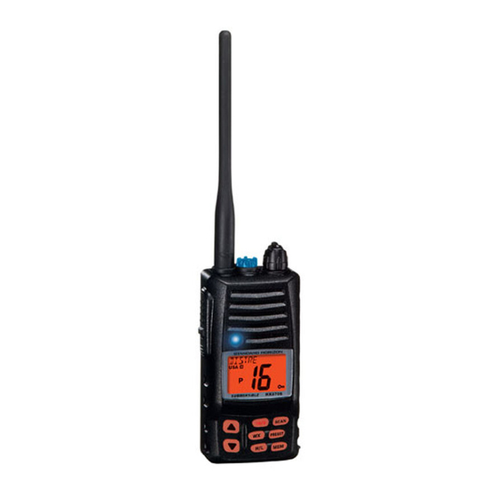
- Page 1 VHF/FM Marine Handheld Transceiver HX370SAS SERVICE MANUAL EM008N95A...
-
Page 2: Specifications
Specifications General Frequency range: 156 MHz - 163.275 MHz (Marine Band + WX Band) Channel Steps: 25 kHz 137 MHz - 174 MHz (LMR) Channel Steps: 12.5 / 25 kHz Frequency stability: ± 2.5 ppm (–22 °F to +140 °F [–30 °C to +60 °C]) Emission type: 16K0G3E, 16K0F3E, 11K0F3E Antenna impedance:... -
Page 3: Exploded View & Miscellaneous Parts
Exploded View & Miscellaneous Parts RA0588600 WINDOW RA058850A RA0401600 DOUBLE FACE TAPE O RING RA058830A RA0577200 (Lot. 1~5) RA058830B (Lot. 5) RA057720A (Lot. 6~) RA058830C (Lot. 6~) LIGHT GUIDE FRONT CASE ASSY RA0588400 FRONT CASE RA0478500 RA0577100 SPECIAL NUT ASSY HOLDER RA057840A RA057700A... - Page 4 Exploded View & Miscellaneous Parts Note:...
- Page 5 Block Diagram...
- Page 6 Connection Diagram...
-
Page 7: Circuit Description
Circuit Description 1. Receive Signal Path 3. Squelch Control Incoming RF from the antenna jack is delivered to the RF The squelch circuitry consists of a noise amplifier and Unit and passes through a low-pass filter consisting of band-pass filter and noise detector within Q1039 coils L1023, L1026, and L1027, capacitors C1227, C1273, (NJM2591V) When no carrier received, noise at the out- C1276, C1270, C1257, and C1256, and antenna switching... -
Page 8: Pll Frequency Synthesizer
Circuit Description If a DCS code is enabled for transmission, the code is gen- The data latch section of Q1017 (MB15A01PFV1) also re- erated by microprocessor Q1066 (HD64F2266) and de- ceives serial dividing data from the microprocessor Q1066 livered to X1001 (21.25 MHz) for DCS modulating. (HD64F2266), which causes the pre-divided VCO signal to be further divided in the programmable divider sec- The modulated signal from the VCO Q1012 (2SC5231) is... -
Page 9: Required Test Equipment
Alignment The HX370SAS has been carefully aligned at the factory Required Test Equipment for the specified performance across the land mobile band. RF Signal Generator with calibrated output level at 200 MHz Realignment should therefore not be necessary except in Deviation Meter (linear detector) the event of a component failure. -
Page 10: Before Alignment
Alignment Before Alignment Squelch Threshold and Tight Squelch Adjustment Press and hold in the [ ] key and [ MEM ] key while Set up the test equipment as shown below for Receiver turning the transceiver on to enter the Alignment Section Alignment. -
Page 11: Transmitter Power Output
Alignment Transmitter Power Output Transmitter Modulation Press the [ ] key to set the display to “dEu dEu.“ The trans- Set up the test equipment as shown below for PLL and Ttransmitter Section Alignment. Maintain the sup- ceiver now is in the Transmitter Modulation Align- ply voltage at 8.4V DC for all steps. - Page 12 Alignment Note:...
- Page 13 MAIN Unit (Lot. 1~7) Circuit Diagram 4.5 V RX: 8.40 V RX: 0 V TX: 8.20 V TX: 2.80 V 3.50 V RX: 0 V TX: 4.60 V 0.67 V 4.30 V RX: 2.90 V RX: 0 V RX: 0 V TX: 2.86 V TX: 3.65 V TX: 1.10 V...
- Page 14 MAIN Unit (Lot. 1~7) Note:...
- Page 15 MAIN Unit (Lot. 1~7) Parts Layout (Side A) HD64F2266 (Q1066) AT24C128N (Q1067) LM2904PWR (Q1062, 1079) CD4094BPWR (Q1053) M62364FP (Q1033) 2SA1774 (FR) 2SC4617 (BR) RD07MVS1 BD4845FVE DTA114TE (94) DTC143ZE (E23) S-812C30AMC UMD2N (D2) DA221 (K) 1SS321 (F9) (Q1022) (Q1004, 1021, (Q1045) (Q1023) (Q1003) (Q1005)
- Page 16 MAIN Unit (Lot. 1~7) Parts Layout (Side B) LM2904PWR LM2902PWR 2SA1774 (FR) 2SC4400 (RT4) 2SJ347 (KS) 2SK3074 (WA) DTA114TE (94) DTA143XE (33) DTA144EE (16) DTC144EE (26) UMW1 (W1) DA221 (K) DAN222 (N) (Q1075, 1078) (Q1074, 1076) (Q1007, 1025, (Q1046) (Q1011, 1048) (Q1036) (Q1002) (Q1029)
- Page 17 MAIN Unit (Lot. 8~) Circuit Diagram...
- Page 18 MAIN Unit (Lot. 8~) Note:...
- Page 19 MAIN Unit (Lot. 8~) Parts Layout (Side A) HD64F2266 (Q1066) AT24C128N (Q1067) LM2904PWR (Q1062, 1079) CD4094BPWR (Q1053) M62364FP (Q1033) 2SA1774 (FR) 2SC4617 (BR) RD07MVS1 BD4845FVE DTA114TE (94) DTC143ZE (E23) S-812C30AMC UMD2N (D2) DA221 (K) 1SS321 (F9) (Q1022) (Q1004, 1021, (Q1045) (Q1023) (Q1003) (Q1005)
- Page 20 MAIN Unit (Lot. 8~) Parts Layout (Side B) LM2904PWR LM2902PWR 2SA1774 (FR) 2SC4400 (RT4) 2SJ347 (KS) 2SK3074 (WA) DTA114TE (94) DTA143XE (33) DTA144EE (16) DTC144EE (26) UMW1 (W1) DA221 (K) DAN222 (N) (Q1075, 1078) (Q1074, 1076) (Q1007, 1025, (Q1046) (Q1011, 1048) (Q1036) (Q1002) (Q1029)
-
Page 21: Main Unit
MAIN Unit Parts List DESCRIPTION VALUE TOL. MFR'S DESIG VXSTD P/N VERS. LOT SIDE LAY ADR PCB with Components CB2717003 DST EXP, IS ON CB2717005 DST USA, IS ON Printed Circuit Board AM008N000 FR011410D FR011410E C 1001 CHIP TA.CAP. 10uF TEMSVA1A106M-8R K78100028 C 1002... - Page 22 MAIN Unit Parts List DESCRIPTION VALUE TOL. MFR'S DESIG VXSTD P/N VERS. LOT SIDE LAY ADR C 1068 CHIP CAP. 0.001uF GRM36B102K50PT K22178809 C 1069 AL.ELECTRO.CAP. 10uF ECEV1HA100SP K48170020 DST:EXP C 1069 AL.ELECTRO.CAP. 10uF ECEV1HA100SP K48170020 DST:USA C 1071 CHIP CAP. 0.1uF GRM36B104K10PT K22108802...
- Page 23 MAIN Unit Parts List DESCRIPTION VALUE TOL. MFR'S DESIG VXSTD P/N VERS. LOT SIDE LAY ADR C 1147 CHIP CAP. 0.1uF GRM36B104K10PT K22108802 C 1148 CHIP CAP. 0.01uF GRM36B103K16PT K22128804 C 1149 CHIP CAP. 0.001uF GRM36B102K50PT K22178809 C 1150 CHIP CAP. 0.001uF GRM36B102K50PT K22178809...
- Page 24 MAIN Unit Parts List DESCRIPTION VALUE TOL. MFR'S DESIG VXSTD P/N VERS. LOT SIDE LAY ADR C 1233 CHIP CAP. UMK105CH060DW-F K22178254 C 1234 CHIP CAP. 15pF UMK105CH150JW-F K22178262 C 1235 CHIP CAP. 15pF UMK105CH150JW-F K22178262 C 1236 CHIP CAP. 0.01uF GRM36B103K16PT K22128804...
- Page 25 MAIN Unit Parts List DESCRIPTION VALUE TOL. MFR'S DESIG VXSTD P/N VERS. LOT SIDE LAY ADR D 1005 DIODE HSC277TRF G2070584 D 1006 DIODE HVC350B-TRF G2070596 D 1007 DIODE HSC277TRF G2070584 D 1009 DIODE HVC350B-TRF G2070596 D 1010 DIODE HVC350B-TRF G2070596 D 1011 DIODE...
- Page 26 MAIN Unit Parts List DESCRIPTION VALUE TOL. MFR'S DESIG VXSTD P/N VERS. LOT SIDE LAY ADR L 1019 M.RFC 150uH FLC32T-151J L1690229 L 1020 M.RFC ELJ-ND1R0JF L1690977 L 1021 M.RFC 0.039uH HK1608 39NJ-T L1690523 L 1022 CHIP COIL 0.082uH LQW1608A82NG00 L1690891 L 1023 COIL...
- Page 27 MAIN Unit Parts List DESCRIPTION VALUE TOL. MFR'S DESIG VXSTD P/N VERS. SIDE LAY ADR Q 1079 LM2904PWR G1094010 Q 1080 TRANSISTOR DTC144EE TL G3070075 R 1003 CHIP RES. 3.3k 1/16W RMC1/16S 332JTH J24189031 R 1004 CHIP RES. 1/16W RMC1/16S 473JTH J24189045 R 1005 CHIP RES.
- Page 28 MAIN Unit Parts List DESCRIPTION VALUE TOL. MFR'S DESIG VXSTD P/N VERS. LOT SIDE LAY ADR R 1072 CHIP RES. 470k 1/16W RMC1/16S 474JTH J24189057 R 1073 CHIP RES. 1/16W RMC1/16S 101JTH J24189013 R 1074 CHIP RES. 100k 1/16W RMC1/16S 104JTH J24189049 R 1075 CHIP RES.
- Page 29 MAIN Unit Parts List DESCRIPTION VALUE TOL. MFR'S DESIG VXSTD P/N VERS. LOT SIDE LAY ADR R 1162 CHIP RES. 330k 1/16W 0.5% MCR01MZPD3303 J24189330 R 1163 CHIP RES. 470k 1/16W 0.5% MCR01MZPD4703 J24189332 R 1164 CHIP RES. 1/16W RMC1/16S 101JTH J24189013 R 1165 CHIP RES.
- Page 30 MAIN Unit Parts List DESCRIPTION VALUE TOL. MFR'S DESIG VXSTD P/N VERS. LOT SIDE LAY ADR R 1238 CHIP RES. 1/16W 0.5% MCR01MZPD1002 J24189374 R 1239 CHIP RES. 1/16W RMC1/16S 103JTH J24189037 R 1241 CHIP RES. 1/16W RMC1/16S 103JTH J24189037 R 1242 CHIP RES.
- Page 31 MAIN Unit Parts List DESCRIPTION VALUE TOL. MFR'S DESIG VXSTD P/N VERS. LOT SIDE LAY ADR R 1323 CHIP RES. 1/16W RMC1/16S 223JTH J24189041 R 1325 CHIP RES. 1/16W RMC1/16S JPTH J24189070 R 1327 CHIP RES. 1/16W RMC1/16S 123JTH J24189038 R 1328 CHIP RES.
- Page 32 MAIN Unit Note:...
- Page 33 Copyright 2005 VERTEX STANDARD CO., LTD. All rights reserved No portion of this manual Marine Division of VERTEX STANDARD may be reproduced without US Headquarters the permission of 10900 Walker Street, Cypress, CA 90630, U.S.A. VERTEX STANDARD CO., LTD.
Need help?
Do you have a question about the HX370SAS and is the answer not in the manual?
Questions and answers