Table of Contents
Advertisement
Quick Links
Download this manual
See also:
Owner's Manual
Advertisement
Table of Contents

Related Manuals for Standard Horizon HX751


Summary of Contents for Standard Horizon HX751
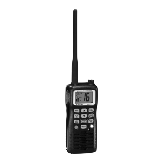
- Page 1 Floating Marine Transceiver HX751 SERVICE MANUAL EM032N97B...
-
Page 2: Specifications
TIA/EIA-603. Important Note The HX751 was assembled using Pb (lead) free solder, based on the RoHS specification. Only lead-free solder (Alloy Composition: Sn-3.0Ag-0.5Cu) should be used for repairs performed on this appara- tus. The solder stated above utilizes the alloy composition required for compliance with the lead-free specification,... -
Page 3: Exploded View & Miscellaneous Parts
SHEET (5.6M-TEX1131) E-DC-19A DC Cable with Cigarette Lighter Plug Q9000821 RA051780B (w/o CE, UK) CAUTION LABEL (FCC) RA1213700 BOTTOM COVER (HX751) RA103720A RA1084800 (x 4 pcs) MASK SHEET (32x28) WASHER 4.3X2.0 CP9173001 (COL:BLAC) CP9173002 (COL:BLUE) BELT CLIP ASSY... - Page 4 Note...
- Page 5 Block Diagram...
- Page 6 Note...
-
Page 7: Circuit Description
Circuit Description 1-3. Squelch Control 1. Receiver Signal Flow Signal components in the neighborhood of 15 kHz con- 1-1. Front-end RF Amplifier tained in the discriminator output pass through an active Received VHF bands signals pass through the low-pass band-pass filter composed of resistors R1211, R1213, & filter/high-pass filter circuit, T/R switch circuit composed R1214, and capacitors C1172 &... -
Page 8: Pll Frequency Synthesizer
Circuit Description 2-2. Modulation 3. PLL Frequency Synthesizer The speech input from the built-in microphone MC1001 PLL IC Q1019 consists of a data shift register, reference (CZ034DP363) or external jack J1001 is pre-emphasized frequency divider, phase comparator, charge pump, in- by C1014 and R1021, and processed by microphone am- termittent operation circuit, and band selector switch. -
Page 9: Required Test Equipment
Alignment The HX751 has been carefully aligned at the factory for Required Test Equipment the specified performance across the land mobile band. RF Signal Generator with calibrated output level at 200 MHz Realignment should therefore not be necessary except in ... -
Page 10: Pll Section
Press the [ CLR/WX ] key again to save the new set- ting. RF Signal AF Signal Generator Generator RF Sampling Inline Wattmeter Coupler Dummy Load HX751 Frequency Counter 7.4 V DC ( ) : Regulated ( ) : BLACK Power Supply... -
Page 11: Transmitter Section
Alignment Noise Squelch Hysteresis Adjustment TX Power Adjustment (Hi Power) Press the [ ] or [ ] key to select Connect the wattmeter and dummy load to the an- HS n xx HS n xx HS n xx”. the display to “HS n xx HS n xx tenna jack. - Page 12 Alignment TX Power Adjustment (Low Power) Connect the wattmeter and dummy load to the an- tenna jack. Set the transceiver to CH16 (156.800 MHz) with “Low” power mode, then turn the transceiver off. Press and hold in the PTT, [ SQL ] , [ ] , and [ ] keys while turn the transceiver on to enter the alignment mode.
- Page 13 MAIN Unit Circuit Diagram 3.3 V 2.0 V TX: 1.2 V TX: 1.9 V RX: 4.5 V RX: 3.0 V 2.1 V TX: 4.3 V TX: 3.4 V TX: 1.7 V RX: 0 V 4.1 V RX: 1.3 V RX: 0 V TX: 0 V RX: 4.5 V 1.8 V...
- Page 14 MAIN Unit Note...
- Page 15 MAIN Unit Parts Layout (Side A) LC87F7BC8A BR24L64F 2SC4617 (BR) S-80835CNMC UMG2N (G2) UMD5N DA221 (K) RB715F (Q1017) (Q1014) (Q1027, 1029) (Q1032) (Q1010) (Q1013) (D1025) (D1039)
- Page 16 MAIN Unit Parts Layout (Side B) LV2105V BU2502FS LM2904PWR 2SA1774 (FR) 2SC4617 (BR) 3SK318 (YB) RD01MUS1 DTC144EE (26) S-812C35AUA UMD5N DA221 (K) (Q1019) (Q1018) (Q1046) (Q1002, 1012, (Q1005, 1015, (Q1035) (Q1033) (Q1011, 1026, (Q1031) (Q1006, 1041, (D1029, 1031, 1016, 1023, 1036) 1024, 1025) 1028, 1047) 1044)
-
Page 17: Main Unit
MAIN Unit Parts List DESCRIPTION VALUE TOL. MFR'S DESIG VXSTD P/N VERS. SIDE LAY ADR PCB with Components CS1990415 DST:USA CS1990416 DST:EXP CS1990417 DST:AUS CS1990418 DST:EU CS1990419 DST:UK Printed Circuit Board AM032N000 FR017580F C 1001 CHIP CAP. 0.033uF GRM155B11A333KA01D K22108803 C 1002 CHIP CAP. - Page 18 MAIN Unit Parts List DESCRIPTION VALUE TOL. MFR'S DESIG VXSTD P/N VERS. SIDE LAY ADR C 1082 CHIP CAP. 39pF GRM1552C1H390JZ01D K22178226 C 1083 CHIP CAP. 6.3V GRM155B30J105KE18D K22088803 C 1084 CHIP CAP. 0.1uF GRM155B11A104KA01D K22108802 C 1085 CHIP CAP. 0.001uF GRM155B11H102KA01D K22178809...
- Page 19 MAIN Unit Parts List DESCRIPTION VALUE TOL. MFR'S DESIG VXSTD P/N VERS. SIDE LAY ADR C 1159 CHIP CAP. 0.0082uF GRM155B11C822KA01D K22128801 C 1160 CHIP CAP. 0.0082uF GRM155B11C822KA01D K22128801 C 1161 CHIP CAP. 15pF GRM1552C1H150JZ01D K22178216 C 1162 CHIP CAP. 0.01uF GRM155B11E103KA01D K22148834...
- Page 20 MAIN Unit Parts List DESCRIPTION VALUE TOL. MFR'S DESIG VXSTD P/N VERS. SIDE LAY ADR C 1236 CHIP CAP. 0.5pF GRP1554C1HR50CZ01E K22178201 C 1237 CHIP CAP. 27pF GRM1552C1H270JZ01D K22178222 C 1238 CHIP CAP. GRM1552C1H6R0DZ01D K22178208 W/ CE LABEL 1- C 1238 CHIP CAP.
- Page 21 MAIN Unit Parts List DESCRIPTION VALUE TOL. MFR'S DESIG VXSTD P/N VERS. SIDE LAY ADR L 1007 M.RFC 0.47uH LK1608 R47K-T L1690414 L 1008 M.RFC 0.068uH HK1608 68NJ-T L1690526 L 1009 M.RFC 0.056uH C1608CB-56NG-RF L1691041 L 1010 M.RFC 0.39uH LK1608 R39K-T L1690413 L 1011 M.RFC...
- Page 22 MAIN Unit Parts List DESCRIPTION VALUE TOL. MFR'S DESIG VXSTD P/N VERS. SIDE LAY ADR R 1004 CHIP RES. 1/16W RMC1/16S 390JTH J24189008 R 1005 CHIP RES. 2.2k 1/16W RMC1/16S 222JTH J24189029 R 1006 CHIP RES. 2.2k 1/16W RMC1/16S 222JTH J24189029 R 1007 CHIP RES.
- Page 23 MAIN Unit Parts List DESCRIPTION VALUE TOL. MFR'S DESIG VXSTD P/N VERS. SIDE LAY ADR R 1089 CHIP RES. 100k 1/16W RMC1/16S 104JTH J24189049 R 1090 CHIP RES. 1/16W RMC1/16S 105JTH J24189061 R 1091 CHIP RES. 100k 1/16W RMC1/16S 104JTH J24189049 R 1092 CHIP RES.
- Page 24 MAIN Unit Parts List DESCRIPTION VALUE TOL. MFR'S DESIG VXSTD P/N VERS. SIDE LAY ADR R 1159 CHIP RES. 1/16W RMC1/16S 103JTH J24189037 R 1160 CHIP RES. 1/16W RMC1/16S 473JTH J24189045 R 1161 CHIP RES. 100k 1/16W RMC1/16S 104JTH J24189049 R 1162 CHIP RES.
- Page 25 MAIN Unit Parts List DESCRIPTION VALUE TOL. MFR'S DESIG VXSTD P/N VERS. SIDE LAY ADR R 1231 CHIP RES. 1/16W RMC1/16S 103JTH J24189037 R 1232 CHIP RES. 1/16W RMC1/16S 103JTH J24189037 R 1233 CHIP RES. 1/16W RMC1/16S 223JTH J24189041 R 1234 CHIP RES.
- Page 26 MAIN Unit Note...
-
Page 27: Charger Cradle
CD-39 Charger Cradle Exploded View RA099690A CASE (CHARGER) CHARGER UNIT : When removing the Charger Unit from the Case, gently pull on the charger unit while pushing the three charging terminals from the outside of the case. RA0997200 (Lot. -
Page 28: Parts Layout
CD-39 Charger Cradle Parts Layout (Side A) (Side B) NJM2904V DTA114EUA 2SC4116 (LG) (Q3001) (Q3009) (Q3004) NJM2360AM DTC114TE (04) RT1N241M (N2) (Lot. 1-4) (Q3007) (Q3002, 3005) DTC124EU (25) (Lot. 5-) (Q3003, 3008) - Page 29 CD-39 Charger Cradle Parts List DESCRIPTION VALUE TOL. MFR'S DESIG VXSTD P/N VERS. SIDE LAY ADR Printed Circuit Board AAF94X000 FR0180800 C 3001 CHIP CAP. 0.1uF GRM188B11C104KA01D K22124805 C 3002 CHIP TA.CAP. 10uF TEESVA1C106M8R K78120077 C 3003 CHIP CAP. 0.1uF GRM21BB11E104KA01L K22140811 C 3004...
- Page 30 Note...
- Page 31 Note...
- Page 32 © 2010 VERTEX STANDARD CO., LTD. All rights reserved. Marine Division of VERTEX STANDARD No portion of this manual US Headquarters may be reproduced 10900 Walker Street, Cypress, CA 90630, U.S.A. without the permission of VERTEX STANDARD CO., LTD.
Need help?
Do you have a question about the HX751 and is the answer not in the manual?
Questions and answers