Table of Contents
Advertisement
IMPORTANT SERVICE NOTES (FOR U.S.A. ONLY) ....................................................................................................... 2
SPECIFICATIONS ............................................................................................................................................................. 2
NAMES OF PARTS ........................................................................................................................................................... 3
OPERATION MANUAL ...................................................................................................................................................... 5
QUICK GUIDE (FOR U.S.A. ONLY) .................................................................................................................................. 6
DISASSEMBLY .................................................................................................................................................................. 7
REMOVING AND REINSTALLING THE MAIN PARTS ................................................................................................... 10
ADJUSTMENT ................................................................................................................................................................. 10
NOTES ON SCHEMATIC DIAGRAM .............................................................................................................................. 13
WAVEFORMS OF CD CIRCUIT ...................................................................................................................................... 14
BLOCK DIAGRAM ........................................................................................................................................................... 15
SCHEMATIC DIAGRAM/WIRING SIDE OF P.W.BOARD ................................................................................................ 18
TROUBLESHOOTING (CD SECTION) ........................................................................................................................... 36
FUNCTION TABLE OF IC ................................................................................................................................................ 41
FL DISPLAY ...................................................................................................................................................................... 48
REPLACEMENT PARTS LIST/EXPLODED VIEW
SERVICE MANUAL
CONTENTS
SHARP CORPORATION
- 1 -
CD-C662
CD-C662 mini component system consisting of CD-C662 (Main unit)
and CP-C662 and (Speaker system).
• In the interests of user-safety the set should be restored to its
original condition and only parts identical to those specified be
used.
This document has been published to be used
for after sales service only.
The contents are subject to change without notice.
CD-C662
No. S4917CDC662//
Page
Advertisement
Table of Contents

Subscribe to Our Youtube Channel
Related Manuals for Sharp CD-C662


Summary of Contents for Sharp CD-C662
-
Page 1: Table Of Contents
SERVICE MANUAL No. S4917CDC662// CD-C662 CD-C662 mini component system consisting of CD-C662 (Main unit) and CP-C662 and (Speaker system). • In the interests of user-safety the set should be restored to its original condition and only parts identical to those specified be used. -
Page 2: Important Service Notes (For U.s.a. Only)
CD-C662 FOR A COMPLETE DESCRIPTION OF THE OPERATION OF THIS UNIT, PLEASE REFER TO THE OPERATION MANUAL. IMPORTANT SERVICE NOTES (FOR U.S.A. ONLY) BEFORE RETURNING THE AUDIO PRODUCT (Fire & Shock Hazard) Before returning the audio product to the user, perform the following safety checks. -
Page 3: Names Of Parts
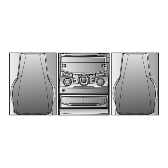
CD-C662 NAMES OF PARTS CD-C662 Front Panel 1. Disc Number Selector Buttons 2. Disc Tray 3. Multi Indicator 4. Disc Skip Button 5. Open/Close Button 6. Extra Bass Indicator 7. FM Stereo Mode Indicator 8. FM Stereo Indicator 12 13 9. - Page 4 CD-C662 CP-C662 Front Speaker 1. Tweeter 2. Woofer 3. Bass Reflex Ducts 4. Speaker Terminals Remote Control 1. Remote Control Transmitter LED CD Control section 2. Disc Number Select Buttons 3. Memory Button 4. Pause Button 5. Clear Button 6. Track Down/Review Button 7.
-
Page 5: Operation Manual
CD-C662 OPERATION MANUAL – 5 –... -
Page 6: Quick Guide (For U.s.a. Only)
CD-C662 – 6 –... -
Page 7: Disassembly
CD-C662 DISASSEMBLY CD-C662 Caution on Disassembly Follow the below-mentioned notes when disassembling Top Cabinet the unit and reassembling it, to keep it safe and ensure Front Panel excellent performance: (A1)x2 1. Take cassette tape and compact disc out of the unit. - Page 8 CD-C662 (L1) x1 ø3 x10mm Front Panel (L2) x1 (E2)x2 Washer (E2)x1 (E3)x1 Turntable (F2)x1 Power Supply Disc Tray Main PWB (M1) x1 ø3 x10mm (E1)x1 ø3x10mm (M2) x1 (F1)x3 Power Amp. ø3x10mm (M1) x1 Main (E2)x1 ø3 x10mm Power Amp.
- Page 9 CD-C662 CP-C662 PROCEDURE STEP REMOVAL FIGURE Front Panel 1. Net ......(A1) x1 2. Rubber ....(A2) x4 3. Screw ..... (A3) x4 4. Tip ......(A4) x2 Woofer 1. Screw ..... (B1) x4 Tweeter 1. Screw ..... (C1) x4...
-
Page 10: Removing And Reinstalling The Main Parts
CD-C662 REMOVING AND REINSTALLING THE MAIN PARTS CD MECHANISM SECTION Loading/Up/Down Perform steps 1, 2, 3, 11, 12, 13, 14 and 15 of the disassembly Motor method to remove the CD mechanism. Motor How to remove the loading motor (See Fig. 10-1) 1. -
Page 11: Tuner Section
CD-C662 • VCO Frequency TUNER SECTION Frequency Frequency Adjusting Instrument fL: Low-range frequency Display Parts Connection fH: High-renge frequency • AM IF/RF 98.00 MHz 98.00 MHz VR351* Pin 13, Pin 21 (60 dB) and ground Signal generator: 400 Hz, 30%, AM modulated of IC303 * Adjust for 76 kHz ±... -
Page 12: Test Mode
CD-C662 TEST MODE • Setting the test mode Any one of test mode can be set by pressing several keys as follows. <REC. PAUSE> + <DISC. SKIP> + <POWER> TEST: CD operation test • TEST mode Function — CD test mode Setting of TEST mode Indication of CD TST mode (Fig. -
Page 13: Notes On Schematic Diagram
CD-C662 NOTES ON SCHEMATIC DIAGRAM • The indicated voltage in each section is the one measured • Resistor: by Digital Multimeter between such a section and the chas- To differentiate the units of resistors, such symbol as K and sis with no signal given. -
Page 14: Waveforms Of Cd Circuit
CD-C662 WAVEFORMS OF CD CIRCUIT STOP PLAY FOCUS SERCH 0.5ms 0.50 V 10.0 V IC1 20 F.E 0.5ms 10.0 V 0.5ms 5.0 V 0.50 V IC1 54 DRF 0.5ms 1.00 V PLAY 0.5ms NORMAL DISC 1.00 V TN0=01 20ms 1.00 V 0.5ms... -
Page 15: Block Diagram
CD-C662 Figure 15 BLOCK DIAGRAM (1/3) – 15 –... - Page 16 CD-C662 SWM3 AM LOOP FOOL PROOF ANTENNA ANTENNA SWM4 F.A.S SOLM1 IC301 FM IF SOLENOID TA7358AP SWM5 CF301 BF301 T301 FM FRONT END FM B.P.F VR351 –B MPX VCO ADJ AM IF T351 CF351 T352 MONO/ST FM OSC FM IF IN...
- Page 17 CD-C662 FL701 DISPLAY Q702 1 2 3 4 37 38 39 Q703 TAPE MOTOR Q705 –B1 Q706 Q707 NO/ST IC563 KIA4558P OPE AMP. IC562 KIA4558P OPE AMP. IC701 IX0280AW –B1 SYSTEM CONTROL MICROCOMPUTER AVDD RX701 UNSWITCH MEMORY BACK UP 9 8 7 6 5 4 3 2 1...
-
Page 18: Schematic Diagram/Wiring Side Of P.w.board
CD-C662 MAIN PWB-A1(2/2) FM SIGNAL C601 CD SIGNAL C602 4.7/50 4.7/50 R601 1.5K R602 1.5K PLAYBACK SIGNAL R603 1.5K R604 1.5K RECORD SUGNAL R605 1.5K R606 1.5K R607 1.5K R608 1.5K C605 C606 4.7/50 4.7/50 C612 0.033 C611 0.033 C613 0.22 C614 0.22... - Page 19 CD-C662 DIGITAL OUTPUT PWB-A4 D_OUT 1 P25 12 - D 100/10 0.022 +4.3V CNP99 TO CD SERVO PWB 2.2µH CNS99 CD GND R639 JK601 R640 R651 R632 C632 R634 L-CH 8.2K 390P R641 VIDEO/AUX R633 R631 C631 R650 8.2K 390P...
- Page 20 CD-C662 DISPLAY PWB-A2 FL701 1 2 3 4 5 6 7 8 9 10 11 12 13 14 15 16 17 18 19 20 21 22 23 24 25 26 27 28 29 30 31 32 FM SIGNAL R722 R721...
- Page 21 CD-C662 P25 7 - G TO CD SERVO PWB CNP12 21 22 23 24 25 26 27 28 29 30 31 32 33 34 35 36 37 38 39 CNS12 1 2 3 4 5 6 7 8 9 1 2 3 4 5 6 7 8 9...
- Page 22 CD-C662 IC901 – STK4113E – POWER AMP. FM SIGNAL C913 R902 C911 R903 R905 D909 Q903 1SS133 KTC3199 GR C912 –B R917 0.1(3W) R909 R919 R906 C923 1.5K 0.022(ML) R915 3.9K R910 Q901 R921 C956 KTC3199 GR 4.7K 47/100 D907...
- Page 23 CD-C662 POWER AMP.PWB-B2 SO901 RL901 SPEAKER L901 TERMINAL 0.29µH D909 Q903 R925 1SS133 KTC3199 GR L-CH 10(1/2W) – 6ohms – R929 R927 10(1/2W) R-CH R932 R935 4.7(1/2W) CNP903 CNS903 220(1/2W) R928 C945 10(1/2W) – R933 47/25 M903 4.7K R936 R926...
- Page 24 CD-C662 47/16 0.01 2SA1318 1/50 64 63 61 60 55 54 53 52 51 50 49 – FIN2 – FIN1 EFBAL – EREF – FOSTA – DGND TOSTA – 2FREQ CNP1 0.1/50 LASER – 0.033 FSTA TE– – LA9241M 100K SERVO AMP.
- Page 25 CD-C662 R57 1K R58 1K R59 1K CD SIGNAL R61 1K R62 1K R63 1K 0.01 64 63 60 59 58 57 56 55 54 53 52 51 50 EFLG SBSY SUB-CODE 16.934 MHz µ-COM INTERFACE DEF1 XVSS X-TAL 3.3M...
- Page 26 CD-C662 P19 12 - C TO MAIN/DECK SECTION R362 C357 3.3/50 C364 FM– 0.015 C366 R367 M/ST 1/50 C356 R CH 3.3/50 L CH R366 C365 1/50 C355 C363 3.3/50 0.015 C354 220P R356 C353 C351 0.018 0.0022 R347 3.9K...
- Page 27 CD-C662 IC301 IC302 IC303 IC701 PIN VOLTAGE NO. VOLTAGE NO. VOLTAGE NO. VOLTAGE VOLTAGE NO. VOLTAGE NO. VOLTAGE NO. VOLTAGE 2.5V 2.5V 0.9V (0V) 2.6V (2.6V) 1.6V (1.7V) 4.8V 4.8V 2.5V 2.6V 1.6V (0V) 0V (0V) 1.6V (1.7V) 4.8V 4.8V 2.5V...
- Page 28 CD-C662 P31 7 - H TO DISPLAY PWB CNS701 FFC701 MAIN PWB-A1 C304 C302 Q344 IC301 R365 R317 R369 R302 R356 4 5 6 7 8 9 10 11 C303 AM LOOP ANTENNA C320 C383 IC302 C308 R313 C309 22 2120 19 18 17 1615 14 13 12...
- Page 29 CD-C662 P31 7 - H O DISPLAY PWB CNS701 P35 12 - E TO CD SERVO CNP11 CNS11 1 2 3 4 5 6 Q109 Q110 Q128 R167 B C E 3 2 1 Q126 B C E C109 1 2 3...
- Page 30 CD-C662 SWITCH PWB-A3 IC703 RS703 SW708 LED707 LED706 LED705 LED704 RS706 RS704 DISC SKIP RS707 SW709 RS705 OPEN/ CLOSE RD09 RS712 DISPLAY PWB-A2 SW729 EQUALIZER R721 R722 R723 C706 SW730 DIMMER C720 C712 IC701 D717 R799 IC704 1 2 3...
- Page 31 CD-C662 SW707 RS703 SW706 LED703 LED702 LED701 DISC3 DISC2 RS701 RS702 FW703 RD06 SW705 DISC1 RD05 FL701 SW704 TIMER/SLEEP RD04 RD03 SW703 CLOCK RX701 RD02 R727 C714 R726 IC701 R701 R702 25 35 R735 R738 R719 SW710 SW701 RD16 POWER...
- Page 32 CD-C662 AC POWER SUPPLY CORD (249) AC120V, 60Hz C801 RL801 T802 POWER TRANSFORMER C802 T801 Q802 POWER TRANSFORMER C820 R804 C818 ZD801 C819 R802 C805 C803 C817 Q801 C812 D807 D806 R801 C809 C804 D809 D808 P30 1 - H...
- Page 33 CD-C662 6ohms R-CH L-CH SO901 SPEAKER TERMINAL R933 R934 1 2 3 Q905 C925 E C B Q903 R930 B C E Q904 C921 R923 R929 C930 C929 R932 R931 D905 R925 R927 D904 D906 R942 ZD902 D909 E C B...
-
Page 34: Tape Mechanism
CD-C662 SWM3 F. P. (260-9) P30 5 - H CNSM1 CNPM1 TO DISPLAY PWB FWM2 FWM1 PHM1 SWM4 CNPM2 F. A. S (260-10) SOLM1 TAPE MECHANISM SOLENOID (260-8) PWB-F SWM5 CAM(260-11) TAPE MOTOR(260-7) TAPE MECHANISM ASSEMBLY TAPE 2 TAPE 1... - Page 35 CD-C662 CD SERVO PWB-C ZD61 16 17 2 3 4 5 CNP10 2 3 4 5 6 7 8 9 10 2 3 4 5 CNS99 IC99 DIGITAL OUTPUT PWB-A4 • The numbers are waveform numbers shown in page 14.
-
Page 36: Troubleshooting (Cd Section)
CD-C662 TROUBLESHOOTING (CD SECTION) When the CD does not function When the CD section does not operate when the objective lens of the optical pickup is dirty, this section may not operate. Clean the objective lens, and check the playback operation. When this section does not operate even after the above step is taken, check the following items. - Page 37 CD-C662 • When the turntable fails to stop. Is from 5 V till 2.5V down pulse (approx. 300 ms) Check the SWM3 and the wiring from the IC701 pin 21 to the 2.5V SWM3. input into the IC701 pin 21 when the turntable is rotating?
- Page 38 CD-C662 • When the CD tray fails to open or close. Check the OPEN CLOSE SW and the wiring from the IC701 Is there following voltage input in specific state of IC701 pin 19? pin 19 to the OPEN CLOSE SW.
- Page 39 CD-C662 • Playback can only be performed when a disc is loaded. Check the laser diode driver. Is the Focus servo active? (Can you hear it working?) Check the area around IC1(16) - (21) (focus servo circuit). If the disc is not turning, the DRF Does the DRF signal change from "L"...
- Page 40 CD-C662 • Checking the spin system. Play operation is performed without disc. The turntable rotates a little. The spin driver circuit is normal. Check the periphery of IC1 pins 23 to 27, pin 39, and pin 40, IC2 The turntable fails to rotate or rotates at high speed.
-
Page 41: Function Table Of Ic
CD-C662 FUNCTION TABLE OF IC IC1 VHiLA9241M/-1: Servo Amp. (LA9241M) (1/2) Function Port Name Pin No. FIN2 Connection pin for photodiode of pickup. RF signal is generated through addition with FIN pin, and FE signal is generated through subtraction. FIN1 Connection pin for photodiode of pickup. - Page 42 CD-C662 IC1 VHiLA9241M/-1:Servo Amp. (LA9241M) (2/2) Function Pin No. Port Name Micro computer command clock input pin. Micro computer command data input pin. Micro computer command chip enable input pin. (DETECT RF) RF level detection output. (Focus Serch Select) Pin to switch focus search mode. (± search/+ search for reference voltage) VCC2 VCC pin for servo system and digital system.
- Page 43 CD-C662 IC2 VHiLC78622N-1: Servo/Signal Control (LC78622N) (1/2) Terminal Name Input/Output Function DEFI Input Defect detection signal (DFF) input terminal. (When this terminal is not used, connect it to 0V.) Input For PLL Input terminal for test. Pull-down resistor built in. Be sure to connect this terminal to 0V.
- Page 44 CD-C662 IC2 VHiLC78622N-1: Servo/Signal Control (LC78622N) (2/2) Terminal Name Input/Output Function SBSY Output Sub-code clock sync signal output terminal. EFLG Output C1, C2, single, double correction monitor terminal. Output Sub-code P, Q, R, S, T, U, and W output terminal.
- Page 45 CD-C662 IC3 VHiM63001FP-1: Focus/Tracking/Spin/Slide Driver (M63001FP) Pin No. Terminal Function IN2– IN6+ Name IN2- CH2 inverted input. IN1A– IN6– IN1A- CH1 inverted input. IN1B– VCC4 IN1B- CH1 output offset control. OUT1- CH1 inverted output. OUT1– OUT6– OUT1+ CH1 non-inverted output.
- Page 46 CD-C662 IC701 RH-iX0301AWZZ:System Microcomputer (IX0301AW) (1/2) Pin No. Port Name Terminal Name Input/Output Function — (+) POWER SUPPLY Output DOLBY PROLOGIC ENABLE TERMINAL Input DATA INPUT Output DATA OUTPUT Output CE OUTPUT Output CLOCK OUTPUT P32, P31 LCK1, LCK2 Output...
- Page 47 CD-C662 IC701 RH-iX0301AWZZ:System Microcomputer (IX0301AW) (2/2) Pin No. Port Name Terminal Name Input/Output Function P116 KEY JOG A Input KEY JOG INPUT A P115 KEY JOG B Input KEY JOG INPUT B P114 S MUTE Output SYSTEM MUTE P113 C MUTE...
-
Page 48: Fl Display
CD-C662 FL701 VVKBJ685GNK-1: FL Display S5 S4 B5 B6 B7 [ 1G~8G ] [ 10G ] ANODE CONNECTION 2G~6G (LOWER) Figure 48 FL DISPLAY – 48 –... -
Page 49: Parts Guide
CD-C662 PARTS GUIDE CD-C662 MODEL CD-C662 mini component system consisting of CD-C662 (Main unit) and CP-C662 and (Speaker system). “HOW TO ORDER REPLACEMENT PARTS” To have your order filled promptly and correctly, please furnish the For U.S.A. only following information. - Page 50 CD-C662 PRICE PRICE PARTS CODE DESCRIPTION PARTS CODE DESCRIPTION RANK RANK LED701 VHPL1154GT4-1 AB LED,Green,L1154GT4 CD-C662 LED702 VHPSLI342YCB1 AC LED,Orange,SLI342YCB LED703 VHPSLI342DCB1 AC LED,Yellow,SLI342DCB INTEGRATED CIRCUITS LED704 VHPSLI342UCB1 AC LED,Red,SLI342UCB LED705 VHPSLI342DCB1 AC LED,Orange,SLI342UCB VHILA9241M/-1 AS Servo Amp.,LA9241M LED706 VHPSLI342YCB1...
- Page 51 CD-C662 PRICE PRICE DESCRIPTION PARTS CODE DESCRIPTION PARTS CODE RANK RANK AB 47 µF,16V,Electrolytic VCEAZA1CW476M J C318 VCCCMN1HH220J J AA 22 pF (CH),50V AA 0.0033 µF,50V AA 0.022 µF,25V VCKYTV1HB332K C319 VCTYMN1EF223Z AA 0.001 µF,50V VCCSPA1HL221J AA 220 pF,50V C320 VCKYPA1HB102K AA 0.0027 µF,50V...
- Page 52 CD-C662 PRICE PRICE PARTS CODE DESCRIPTION PARTS CODE DESCRIPTION RANK RANK AC 100 µF,35V,Electrolytic C820 VCEAZA1VW107M J VRD-ST2CD102J AA 1 kohm,1/6W AG 3300 µF,25V,Electrolytic C850 VCEAZW1EW338M J VRS-TV2AB221J AA 220 ohms,1/10W AB 22 µF,25V,Electrolytic C851 VCEAZA1EW226M J R71,72 VRD-ST2CD272J AA 2.7 kohms,1/6W AB 0.047 µF,50V,Mylar...
- Page 53 CD-C662 PRICE PRICE DESCRIPTION PARTS CODE DESCRIPTION PARTS CODE RANK RANK R555 VRD-ST2CD563J AA 56 kohms,1/6W R851 VRD-ST2CD330J AA 33 ohms,1/6W R556 VRD-MN2BD333J AA 33 kohms,1/8W R852,853 VRD-ST2CD223J AA 22 kohms,1/6W R558 VRD-ST2CD683J AA 68 kohms,1/6W R854 VRD-ST2CD103J AA 10 kohm,1/6W...
- Page 54 CD-C662 PRICE PRICE PARTS CODE DESCRIPTION PARTS CODE DESCRIPTION RANK RANK CNP101 92LCONE3P53253 J AB Plug,3Pin SWM4(260-10) QSW-F9003AWZZ AG Switch,Leaf Type [F.A.S.] CNP102 92LCONE7P53253 J AC Plug,7Pin SWM5(260-11) 92LM-SW1658A AB Switch,Leaf Type [CAM] CNP301 92LCONE-3P5268 AC Plug,3Pin CD MECHANISM PARTS...
- Page 55 CD-C662 PRICE PRICE DESCRIPTION PARTS CODE DESCRIPTION PARTS CODE RANK RANK NGERK0004AWZZ J AB Gear,Bevel XEBSD26P12000 AA Screw,ø2.6×12mm NGERK0005AWZZ J AB Gear,Loading XHBSD30P06000 AA Screw,ø3×6mm NGERW0006AWZZ J AC Gear,Worm Wheel XJBSF30P06000 AA Screw,ø3×6mm NPLYD0002AWZZ AC Pulley XEBSF30P10000 AA Screw,ø3×10mm LANGF0032AWZZ...
- Page 56 CD-C662 CD-C662 306-2 306-1 306-3 703x2 703x2 305x2 PWB-D Figure 7 CD MECHANISM EXPLODED VIEW – 7 – – 56 –...
- Page 57 CD-C662 CD-C662 623x2 610x2 PWB-A3 622x3 608x2 240-1 601x5 PWB-A2 PWB-A4 240-2 610x11 FL701 PWB-A1 202-14 202-15 603x3 202-10 202-13 202-2 202-11 Q852 202-7 202-6 Q851 608x2 Q850 202-5 202-4 202-12 202-3 202-21 Silicon 202-18 Grease PWB-F 202-20 202-17 202-8...
- Page 58 CD-C662 CD-C662 208-3 208-2 601x2 208-1 233-3 601x2 233-2 233-1 233-4 229x2 MECHANISM 617x2 616x4 PWB-C PWB-E SOLM2 Figure 9 CABINET EXPLODED VIEW (2/2) – 58 – – 9 –...
- Page 59 CD-C662 CP-C662 (with 907x4 Capacitor C1,2) SP3,4 909x4 911x4 908x4 SP1,2 TWEETER SP3(L-CH) SP4(R-CH) 908x4 C1,2 Capacitor TWEETER C1,2 SP3(L-CH) Capacitor SP4(R-CH) 3.3µF,100V, WOOFER Electrolytic (N.P.) SP1(L-CH) WOOFER SP2(R-CH) SP1(L-CH) SP2(R-CH) Figure 10 SPEAKER EXPLODED VIEW – 10 – – 59 –...
-
Page 60: Packing Of The Set (For U.s.a. Only)
Packing Case 92L416-0064 Center Pad Not Replacement Item © COPYRIGHT 1999 BY SHARP CORPORATION SHARP CORPORATION ALL RIGHTS RESERVED. Communication Systems Group No part of this publication may be reproduced, Quality & Reliability Control Center stored in a retrieval system, or transmitted in...
Need help?
Do you have a question about the CD-C662 and is the answer not in the manual?
Questions and answers