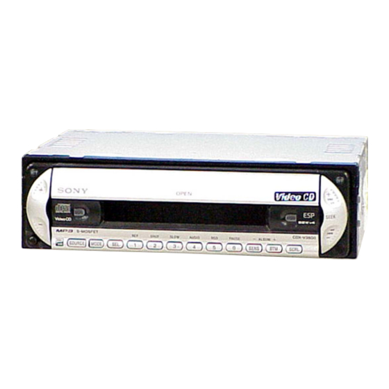
Sony CDX-V3800 Service Manual
Fm/am multi media player
Hide thumbs
Also See for CDX-V3800:
- Service manual (66 pages) ,
- Operating instructions manual (72 pages)
Table of Contents
Advertisement
SERVICE MANUAL
Ver. 1.3 2006.05
• The tuner and CD sections have no adjustments.
CD player section
Signal-to-noise ratio
90 dB
Frequency response
10 – 20,000 Hz
Wow and flutter
Below measurable limit
Signal format system
PAL/NTSC
Tuner section
FM
Tuning range
FM tuning interval:
50 kHz/200 kHz
switchable
87.5 – 108.0 MHz
(at 50 kHz step)
87.5 – 107.9 MHz
(at 200 kHz step)
Aerial terminal
External aerial connector
Intermediate frequency
10.7 MHz/450 kHz
Usable sensitivity
9 dBf
Selectivity
75 dB at 400 kHz
Signal-to-noise ratio
67 dB (stereo),
69 dB (mono)
Harmonic distortion at 1 kHz
0.5% (stereo),
0.3% (mono)
Separation
35 dB at 1 kHz
Frequency response
30 – 15,000 Hz
AM
Tuning range
AM tuning interval:
9 kHz/10 kHz switchable
531 – 1,602 kHz
(at 9 kHz step)
530 – 1,710 kHz
(at 10 kHz step)
Aerial terminal
External aerial connector
Intermediate frequency
10.7 MHz/450 kHz
Sensitivity
30 µV
Sony Corporation
9-879-406-04
2006E04-1
eVehicle Division
© 2006.05
Published by Sony Techno Create Corporation
CDX-V3800
Model Name Using Similar Mechanism
CD Drive Mechanism Type
Optical Pick-up Name
SPECIFICATIONS
Power amplifier section
Outputs
Speaker impedance
Maximum power output 52 W × 4 (at 4 ohms)
General
Outputs
Inputs
Tone controls
Power requirements
Dimensions
Mounting dimensions
Mass
Supplied accessories
Design and specifications are subject to change without
notice.
FM/AM MULTI MEDIA PLAYER
E Model
Chinese Model
NEW
MG-611MM-186//K
KSS1000E
Speaker outputs
(sure seal connectors)
4 – 8 ohms
Audio output terminals (front, rear/sub switchable)
Video output terminal
Power aerial relay control terminal
Power amplifier control terminal
AUX IN terminal
Parking break control terminal
Aerial input terminal
Low:
±10 dB at 60 Hz (XPLOD)
Mid:
±10 dB at 1 kHz (XPLOD)
High:
±10 dB at 10 kHz (XPLOD)
12 V DC car battery
(negative earth)
Approx. 178 × 50 × 179 mm (w/h/d)
Approx. 182 × 53 × 161 mm (w/h/d)
Approx. 1.2 kg
Parts for installation and connections (1 set)
Front panel case (1)
Card remote commander RM-X158
1
Advertisement
Chapters
Table of Contents

Subscribe to Our Youtube Channel
Related Manuals for Sony CDX-V3800


Summary of Contents for Sony CDX-V3800
-
Page 1: Specifications
(at 9 kHz step) 530 – 1,710 kHz (at 10 kHz step) Aerial terminal External aerial connector Intermediate frequency 10.7 MHz/450 kHz Sensitivity 30 µV FM/AM MULTI MEDIA PLAYER Sony Corporation 9-879-406-04 2006E04-1 eVehicle Division © 2006.05 Published by Sony Techno Create Corporation... - Page 2 COMPONENTS IDENTIFIED BY MARK 0 OR DOTTED LINE WITH MARK 0 ON THE SCHEMATIC DIAGRAMS AND IN THE PARTS LIST ARE CRITICAL TO SAFE OPERATION. REPLACE THESE COMPONENTS WITH SONY PARTS WHOSE PART NUMBERS APPEAR AS SHOWN IN THIS MANUAL OR IN SUPPLEMENTS PUBLISHED BY SONY.
- Page 3 CDX-V3800 Notes on CD-Rs (recordable CDs)/CD-RWs (rewritable UNLEADED SOLDER CDs) Boards requiring use of unleaded solder are printed with the lead This unit can play the following discs: free mark (LF) indicating the solder contains no lead. (Caution: Some printed circuit boards may not come printed with the lead free mark due to their particular size.)
-
Page 4: Table Of Contents
CDX-V3800 TABLE OF CONTENTS 1. GENERAL Location of Controls ..............5 Connections ................5 2. DISASSEMBLY 2-1. Sub Panel (1) Assy .............. 8 2-2. CD Mechanism Block ............8 2-3. Main Board ................. 9 2-4. Chassis (T) Sub Assy ............9 2-5. -
Page 5: General
CDX-V3800 SECTION 1 GENERAL This section is extracted from instruction manual. Selecting an album with the card Card remote commander RM-X158 Location of controls remote commander Album can be skipped using M (+)/m (–) on the card remote commander. Refer to the pages listed for details. - Page 6 CDX-V3800...
-
Page 7: Disassembly
CDX-V3800 SECTION 2 DISASSEMBLY Note : This set can be disassemble according to the following sequence. 2-1. SUB PANEL (1) ASSY (Page 8) 2-2. CD MECHANISM BLOCK (Page 8) 2-10. SERVO BOARD 2-3. MAIN BOARD 2-4. CHASSIS (T) SUB ASSY... - Page 8 CDX-V3800 Note : Follow the disassembly procedure in the numerical order given. 2-1. SUB PANEL (1) ASSY 3 two claws 2 two claws 1 two screws (+PTT 2.6 x 6) 4 sub panel (1) assy 2-2. CD MECHANISM BLOCK 8 bracket (CD)
-
Page 9: Main Board
CDX-V3800 2-3. MAIN BOARD 5 screw (+PTT 2.6 x 8) 6 connection (video out) cord 1 three screws (+BTT ) 2 two screws (+PTT 2.6 x 8) 3 MAIN board 4 insulating sheet 2-4. CHASSIS (T) SUB ASSY 4 claw 2 two screws (+P 1.7 x 2.2) -
Page 10: Roller Arm Assy
CDX-V3800 2-5. ROLLER ARM ASSY 3 washer (1.1-2.5) 5 roller arm assy 4 gear (RA1) 2 spring (RAR) 1 spring (RAL) 2-6. CHASSIS (OP) ASSY qa chassis (OP) assy 0 coil spring (damper) lever (D) 4 washer 1 CN500 (16P) -
Page 11: Optical Pick-Up
CDX-V3800 2-7. OPTICAL PICK-UP 2 chucking arm sub assy 5 claw 1 tension coil spring (CHKG) 7 optical pick-up 6 main shaft 4 rack (SL) 3 screw (+B 1.4 x 5) 2-8. SL MOTOR ASSY (M902) 1 screw (+P 1.4 x 1.8) -
Page 12: Le Motor Assy (M903)
CDX-V3800 2-9. LE MOTOR ASSY (M903) 8 screw 0 gear (LE) assy (+M 1.7 x 2.5) 9 bearing (LEB-N) 2 washer qa screw (+M 1.7 x 2.5) qf two toothed lock screws 3 gear (LE1) (+M 1.4 ) lever (D) -
Page 13: Diagrams
CDX-V3800 SECTION 3 DIAGRAMS 3-1. BLOCK DIAGRAM — CD SECTION — DIGITAL DIGITAL SIGNAL PROCESSOR MODULATOR IC100 IC700 MAIN CD-L 2 DIN LOUT AU DATA SECTION (Page 14) ROUT R-CH DETECTOR AU LRCK 1 LRCK AU BCK 3 BCKIN 14 SCKI... -
Page 14: Block Diagram -Main Section
CDX-V3800 3-2. BLOCK DIAGRAM — MAIN SECTION — ELECTRONIC VOLUME IC401 AUX IN R-CH R-CH OUTS2 REAR PJ401 OUTS1 R-CH AUDIO OUT R-CH CD-L 9 C2 SECTION R-CH 8 C1 (Page 13) FRONT AUDIO OUT R-CH TUX601 POWER AMP MUTE... -
Page 15: Block Diagram -Display Section
CDX-V3800 3-3. BLOCK DIAGRAM — DISPLAY SECTION — 3-4. CIRCUIT BOARDS LOCATION SYSTEM CONTROL LCD DRIVER IC801 (3/3) IC501 S522 (OPEN) SERVO board SHUT SW LCD501 SEG3 SENSOR board LIQUID LCD SO SEG50 SPEAKER board CRYSTAL • LCD SCK DISPLAY... - Page 16 CDX-V3800 Ver. 1.3 • NOTE FOR PRINTED WIRING BOARDS AND SCHEMATIC DIAGRAMS • WAVEFORMS — Servo Board — (MODE: CD PLAY) — Main Board — THIS NOTE IS COMMON FOR PRINTED WIRING BOARDS AND SCHEMATIC DIAGRAMS. IC500 rd (XO) IC801 i; (XOA) (In addition to this, the necessary note is printed in each block.)
-
Page 17: Printed Wiring Boards -Cd Mechanism Section
CDX-V3800 3-5. PRINTED WIRING BOARDS — CD MECHANISM SECTION — • Refer to page 15 for Circuit Boards Location. : Uses unleaded solder. L401 C401 R111 CN401 D906 FB503 C305 C304 C303 C302 C402 R631 C408 FMB6 R401 R402 IC200... -
Page 18: Schematic Diagram -Cd Mechanism Section (1/2)
CDX-V3800 Ver. 1.3 • Refer to page 16 for Waveforms. 3-6. SCHEMATIC DIAGRAM — CD MECHANISM SECTION (1/2) — • Refer to page 26 for IC Block Diagrams. • Refer to page 27 for IC Pin Description of IC500. R547... -
Page 19: Schematic Diagram -Cd Mechanism Section (2/2)
CDX-V3800 • Refer to page 16 for Waveform. 3-7. SCHEMATIC DIAGRAM — CD MECHANISM SECTION (2/2) — • Refer to page 26 for IC Block Diagram. • Refer to page 29 for IC Pin Description of IC400. L401 C401 IC B/D... -
Page 20: Printed Wiring Boards -Main Section
CDX-V3800 3-8. PRINTED WIRING BOARDS — MAIN SECTION — • Refer to page 15 for Circuit Boards Location. : Uses unleaded solder. PJ401 C436 C435 C434 C433 C439 C993 CNP901 C994 PJ601 R442 C113 JW111 R443 F901 R421 R418 C991... - Page 21 CDX-V3800 3-9. SCHEMATIC DIAGRAM — MAIN SECTION (1/3) — • Refer to page 26 for IC Block Diagram. C433 C434 C435 C436 R425 C439 R426 PJ601 R430 C443 R468 R428 R302 C303 D301 IC B/D R416 C424 IC401 C421 R421...
-
Page 22: Schematic Diagram -Main Section (1/3)
CDX-V3800 3-10. SCHEMATIC DIAGRAM — MAIN SECTION (2/3) — C113 C101 C107 D921 D922 CNP901 IC100 C993 C991 FB901 FB902 R931 R932 R913 F901 D914 C990 C994 D918 L900 C111 C106 (Page 21) C992 C109 C922 C446 R447 C447 C441... -
Page 23: Schematic Diagram -Main Section (3/3)
CDX-V3800 • Refer to page 16 for Waveforms. 3-11. SCHEMATIC DIAGRAM — MAIN SECTION (3/3) — • Refer to page 30 for IC Pin Description of IC801. (Page 21) (Page 22) C810 C809 R901 R828 R925 R830 R813 R821 R823... -
Page 24: Printed Wiring Board -Display Section
CDX-V3800 3-12. PRINTED WIRING BOARD — DISPLAY SECTION — • Refer to page 15 for Circuit Boards Location. : Uses unleaded solder. S507 LED507, S509 S513 S503 LED521 LED521, LED503 LED517 S507 (CD WINDOW) S516 S515 (VOLUME) S522 (OPEN) LED513... -
Page 25: Schematic Diagram -Display Section
CDX-V3800 3-13. SCHEMATIC DIAGRAM — DISPLAY SECTION — R552 R571 R573 R575 R577 R579 LED503 LED501 R551 R533 LED515 LED512 LED509 LED505 LED513 IC502 R537 C551 R532 CN901 R536 R531 C960 LED518 LED510 LED522 LED521 LED502 LED517 IC501 R553 LED514... - Page 26 CDX-V3800 • IC BLOCK DIAGRAMS IC700 WM8726GED/R (SERVO Board (1/2)) IC400 SPCA717A-HL211 (SERVO Board (2/2)) LRCIN SCKI SERIAL FORMAT INTERFACE IC500 BU9536KS2 (SERVO Board (1/2)) 32 31 30 29 28 27 26 25 BCKIN DATA7 DEEMPH FSADJUST DIGITAL LATCH DATA6...
- Page 27 CDX-V3800 • IC PIN DESCRIPTIONS • IC500 BU9536KS2 (RF AMP, DIGITAL SERVO) (SERVO BOARD (1/2)) Pin No. Pin Name Pin Description AVDD1 — Analog power supply pin (+3.3 V) A+C voltage signal input from optical pick-up block B+D voltage signal input from optical pick-up block...
- Page 28 CDX-V3800 Pin No. Pin Name Pin Description Tracking error amplifier feedback signal input CAGC RFAGC capacitor install pin RF signal input RF equalizer signal output...
- Page 29 CDX-V3800 • IC400 SPCA717A-HL211 (VIDEO SIGNAL PROCESSOR) (SERVO BOARD (2/2)) Pin No. Pin Name Pin Description Full-Scale adjust control pin The Full-Scale current of D/A converters can be FSADJUST — adjusted by connecting a resistor (RESET) between this pin and ground.
- Page 30 CDX-V3800 • IC801 MB90488BPF-G-135-BNDE1 (SYSTEM CONTROL) (MAIN BOARD (3/3)) Pin No. Pin Name Pin Description LINE ATT Audio mute control signal output 2 to 4 — Not used in this set. (Open) BEEP Beep signal output to power amp IC...
- Page 31 CDX-V3800 Pin No. Pin Name Pin Description ACC IN Accessory power supply detect signal input SIRCS Remote control signal (infrared rays) input — Not used in this set. (Fixed at “L”.) PAK BK Test mode detect signal input Memory mode changeover signal input FLASH W Normally “H”...
-
Page 32: Exploded Views
CDX-V3800 SECTION 4 EXPLODED VIEWS NOTE: • The mechanical parts with no reference • Color Indication of Appearance Parts The components identified by mark 0 or dotted line with mark number in the exploded views are not supplied. Example : 0 are critical for safety. -
Page 33: Front Panel Section
CDX-V3800 4-2. FRONT PANEL SECTION not supplied (DISPLAY board) not supplied LCD501 not supplied not supplied supplied not supplied not supplied not supplied not supplied Ref. No. Part No. Description Remark Ref. No. Part No. Description Remark X-2024-914-1 PANEL (BASE) ASSY, FRONT... -
Page 34: Cd Mechanism Section (1)
CDX-V3800 4-3. CD MECHANISM SECTION (1) (MG-611MM-186//K) not supplied (SENSOR board) not supplied not supplied not supplied not supplied Ref. No. Part No. Description Remark Ref. No. Part No. Description Remark A-3372-455-A CHASSIS (T) SUB ASSY 2-345-767-01 SPRING (KF60), TENSION... -
Page 35: Cd Mechanism Section (2)
CDX-V3800 4-4. CD MECHANISM SECTION (2) (MG-611MM-186//K) (including M901) M902 not supplied not supplied not supplied not supplied The components identified by mark 0 or dotted line with mark 0 are critical for safety. Replace only with part number specified. -
Page 36: Cd Mechanism Section (3)
CDX-V3800 4-5. CD MECHANISM SECTION (3) (MG-611MM-186//K) M903 Ref. No. Part No. Description Remark Ref. No. Part No. Description Remark 3-262-755-01 WASHER (1.1-2.5) 2-186-696-11 BRACKET (LEM-N) 2-186-699-11 GEAR (RA1) 3-345-648-91 SCREW (M1.4), TOOTHED LOCK A-1075-789-A ARM ASSY, ROLLER A-1083-637-A GEAR (LE) ASSY... -
Page 37: Cd Mechanism Section (4)
CDX-V3800 4-6. CD MECHANISM SECTION (4) (MG-611MM-186//K) Ref. No. Part No. Description Remark Ref. No. Part No. Description Remark 2-186-700-11 GEAR (CHK1) 3-899-829-01 WASHER (SLIT) 3-344-223-01 WASHER 3-259-032-01 GEAR (LE2) 3-259-470-01 GEAR (LE1) A-1075-791-A CHASSIS (M) BLOCK ASSY 3-253-755-02 LEVER (D) -
Page 38: Electrical Parts List
CDX-V3800 SECTION 5 DISPLAY ELECTRICAL PARTS LIST NOTE: • Due to standardization, replacements in • Items marked “*” are not stocked since The components identified by mark 0 or dotted line with mark the parts list may be different from the they are seldom required for routine service. - Page 39 CDX-V3800 DISPLAY MAIN Ref. No. Part No. Description Remark Ref. No. Part No. Description Remark R557 1-216-821-11 METAL CHIP 1/10W C409 1-115-467-11 CERAMIC CHIP 0.22uF R558 1-216-821-11 METAL CHIP 1/10W C410 1-126-960-11 ELECT R559 1-216-821-11 METAL CHIP 1/10W C411 1-126-960-11 ELECT...
- Page 40 CDX-V3800 MAIN Ref. No. Part No. Description Remark Ref. No. Part No. Description Remark C908 1-123-611-61 ELECT IC801 6-805-155-01 IC MB90488BPF-G-135-BNDE1 C922 1-131-868-81 ELECT 3300uF IC802 8-759-659-13 IC PST3428UL C990 1-115-340-11 CERAMIC CHIP 0.22uF C991 1-115-340-11 CERAMIC CHIP 0.22uF < JUMPER RESISTOR >...
- Page 41 CDX-V3800 MAIN SENSOR Ref. No. Part No. Description Remark Ref. No. Part No. Description Remark R417 1-216-809-11 METAL CHIP 1/10W R830 1-216-809-11 METAL CHIP 1/10W R418 1-216-841-11 METAL CHIP 1/10W R832 1-216-825-11 METAL CHIP 2.2K 1/10W R419 1-216-841-11 METAL CHIP...
- Page 42 CDX-V3800 SERVO Ref. No. Part No. Description Remark Ref. No. Part No. Description Remark A-1107-620-A SERVO BOARD, COMPLETE C519 1-162-964-11 CERAMIC CHIP 0.001uF C521 1-162-970-11 CERAMIC CHIP 0.01uF ********************** C531 1-126-208-21 ELECT CHIP 47uF < CAPACITOR > C540 1-107-826-11 CERAMIC CHIP 0.1uF...
- Page 43 CDX-V3800 SERVO Ref. No. Part No. Description Remark Ref. No. Part No. Description Remark R103 1-218-933-11 RES-CHIP 1/16W R546 1-218-953-11 RES-CHIP 1/16W R104 1-218-933-11 RES-CHIP 1/16W R547 1-243-975-81 METAL CHIP 4.7M 1/16W R105 1-218-933-11 RES-CHIP 1/16W R548 1-218-959-11 RES-CHIP 3.3K...
- Page 44 CDX-V3800 Ref. No. Part No. Description Remark MISCELLANEOUS *************** 1-829-847-11 CABLE, FLAT (FFC) 26P 1-792-194-61 CORD (WITH CONNECTOR) (POWER) 1-829-836-12 CORD, CONNECTION (VIDEO OUT) 0 153 8-820-207-12 OPTICAL PICK-UP (KSS1000E/K1RP) A-1075-787-A CHASSIS (OP) SUB ASSY (including M901) F901 1-532-877-11 FUSE (BLADE TYPE) (AUTO FUSE) 10A...
- Page 45 File this supplement with the service manual. Subject : Production country change. The CDX-V3800 model has been changed in the production country to Thailand from Korea. This service manual, SUPPLEMENT-1 only contains the change. When servicing and inspecting, check the Model Number Label to see if the model is made in Thailand or Korea.
- Page 46 CDX-V3800 TABLE OF CONTENTS 1. DIAGRAMS 1-1. Printed Wiring Boards –Main Section– ......4 1-2. Schematic Diagram –Main Section (1/3)– ......5 1-3. Schematic Diagram –Main Section (2/3)– ......6 1-4. Schematic Diagram –Main Section (3/3)– ......7 1-5. Printed Wiring Board –Key Section– ........8 1-6.
-
Page 47: Diagrams
CDX-V3800 SECTION 1 DIAGRAMS • NOTE FOR PRINTED WIRING BOARDS AND SCHEMATIC DIAGRAMS • WAVEFORMS THIS NOTE IS COMMON FOR PRINTED WIRING — Main Board — BOARDS AND SCHEMATIC DIAGRAMS. (In addition to this, the necessary note is printed IC801 i; (XOA) in each block.) -
Page 48: Printed Wiring Boards -Main Section
CDX-V3800 1-1. PRINTED WIRING BOARDS — MAIN SECTION — : Uses unleaded solder. PJ401 PJ601 C436 C434 C433 C435 C993 C994 R442 JW111 R443 F900 R421 R418 C113 IC100 C991 R427 C990 CNP901 C437 C443 C440 C439 R431 JW109 JW98... - Page 49 CDX-V3800 1-2. SCHEMATIC DIAGRAM — MAIN SECTION (1/3) — • Refer to page 10 for IC Block Diagrams. C433 C434 C435 C436 R425 R426 C439 PJ601 R468 R428 R430 C443 C108 D301 IC B/D C424 R416 IC401 C421 R421 Q405...
-
Page 50: Schematic Diagram -Main Section (1/3)
CDX-V3800 1-3. SCHEMATIC DIAGRAM — MAIN SECTION (2/3) — C113 C101 C107 D921 D922 CNP901 IC100 C993 C991 FB901 FB902 R931 R932 R913 F900 D914 C990 C994 D918 L900 C111 C106 (Page 5) C992 C922 C109 C446 R447 C447 C441... -
Page 51: Schematic Diagram -Main Section (3/3)
CDX-V3800 1-4. SCHEMATIC DIAGRAM — MAIN SECTION (3/3) — • Refer to page 3 for Waveforms. (Page 6) (Page 5) C810 C809 R901 C604 R828 R925 R830 R813 R821 R823 D701 R822 CN751 C707 C709 R708 R834 R832 D820 R709... -
Page 52: Printed Wiring Board -Key Section
CDX-V3800 1-5. PRINTED WIRING BOARD — KEY SECTION — : Uses unleaded solder. LED507 S513 LED507, S509 S507 LED503 S509 S503 (CD WINDOW) LED521 LED517 LED521, LED503 S507 S516 S515 (VOLUME) LED513 LED514 LED501 LED502 LED516 LED520, LED520 S514 S508... -
Page 53: Schematic Diagram -Key Section
CDX-V3800 1-6. SCHEMATIC DIAGRAM — KEY SECTION — R552 LED503 LED501 R571 R573 R575 R577 R579 R551 R533 LED515 LED512 LED509 LED505 LED513 IC502 C551 R532 CN901 R538 R531 C960 LED518 LED510 LED522 LED521 LED517 R537 R536 IC501 R553 S522... - Page 54 CDX-V3800 • IC BLOCK DIAGRAMS IC401 BD3806FS-E2 (MAIN Board (1/3)) FADER FADER FADER FADER (0~-58, (0~-58, (0~-58, (0~-58, C BUS -∞dB) -∞dB) -∞dB) -∞dB) GAIN+ATT LOGIC (+10~-29, -∞dB) EFFECT (0dB~ EFFECT (0dB~ 2ND ORDER LPF +20dB,2dB STEP) +20dB,2dB STEP) fc:OFF,80,120,160Hz 2ND ORDER Q: 0.707...
-
Page 55: Exploded Views
CDX-V3800 SECTION 2 EXPLODED VIEWS NOTE: • The mechanical parts with no reference • Color Indication of Appearance Parts The components identified by mark 0 or dotted line with mark number in the exploded views are not supplied. Example : 0 are critical for safety. -
Page 56: Front Panel Section
CDX-V3800 2-2. FRONT PANEL SECTION not supplied (KEY board) not supplied LCD501 not supplied not supplied supplied not supplied supplied not supplied not supplied not supplied not supplied not supplied Ref. No. Part No. Description Remark Ref. No. Part No. -
Page 57: Cd Mechanism Section (1)
CDX-V3800 2-3. CD MECHANISM SECTION (1) (MG-611MM-186//Q) not supplied (SENSOR board) not supplied not supplied Ref. No. Part No. Description Remark Ref. No. Part No. Description Remark A-3372-444-A CHASSIS (T) SUB ASSY 2-587-505-01 SCREW 3-253-729-11 SPRING (LTR), TENSION COIL A-1107-620-A SERVO BOARD, COMPLETE... -
Page 58: Cd Mechanism Section (2)
CDX-V3800 2-4. CD MECHANISM SECTION (2) (MG-611MM-186//Q) (including M901) M902 not supplied not supplied not supplied not supplied not supplied Ref. No. Part No. Description Remark Ref. No. Part No. Description Remark A-1075-644-A CHASSIS (OP) COMPLETE ASSY A-3372-446-A LEVER (SL) SUB ASSY 3-316-938-91 SCREW (B1.4X5), TAPPING... -
Page 59: Cd Mechanism Section (3)
CDX-V3800 2-5. CD MECHANISM SECTION (3) (MG-611MM-186//Q) M903 Ref. No. Part No. Description Remark Ref. No. Part No. Description Remark 3-348-993-01 WASHER 2-186-696-01 BRACKET (LEM-N) 2-186-699-01 GEAR (RA1) 3-345-648-91 SCREW (M1.4), TOOTHED LOCK A-1075-641-B ARM ASSY, ROLLER A-1083-636-A GEAR (LE) ASSY... -
Page 60: Cd Mechanism Section (4)
CDX-V3800 2-6. CD MECHANISM SECTION (4) (MG-611MM-186//Q) Ref. No. Part No. Description Remark Ref. No. Part No. Description Remark 2-186-700-01 GEAR (CHK1) 2-630-962-01 WASHER (SLIT) 3-344-223-01 WASHER * 256 2-590-545-01 GEAR (LE2-M) 3-259-470-11 GEAR (LE1) A-1075-640-B CHASSIS (M) BLOCK ASSY... -
Page 61: Electrical Parts List
CDX-V3800 SECTION 3 ELECTRICAL PARTS LIST NOTE: • Due to standardization, replacements in • Items marked “*” are not stocked since The components identified by mark 0 or dotted line with mark the parts list may be different from the they are seldom required for routine service. - Page 62 CDX-V3800 MAIN Ref. No. Part No. Description Remark Ref. No. Part No. Description Remark R555 1-216-821-11 METAL CHIP 1/10W C408 1-115-467-11 CERAMIC CHIP 0.22uF R557 1-216-821-11 METAL CHIP 1/10W C409 1-115-467-11 CERAMIC CHIP 0.22uF R558 1-216-821-11 METAL CHIP 1/10W C410...
- Page 63 CDX-V3800 MAIN Ref. No. Part No. Description Remark Ref. No. Part No. Description Remark C821 1-107-826-11 CERAMIC CHIP 0.1uF < IC > C822 1-107-826-11 CERAMIC CHIP 0.1uF C825 1-104-665-11 ELECT 100uF IC100 6-705-360-02 IC TDA8588BJ/N2/R1 C908 1-123-611-61 ELECT IC401 6-705-372-01 IC BD3808FS-FE2...
- Page 64 CDX-V3800 MAIN Ref. No. Part No. Description Remark Ref. No. Part No. Description Remark R413 1-216-864-11 SHORT CHIP R824 1-216-849-11 METAL CHIP 220K 1/10W R414 1-216-809-11 METAL CHIP 1/10W R825 1-216-849-11 METAL CHIP 220K 1/10W R415 1-216-809-11 METAL CHIP 1/10W...
- Page 65 CDX-V3800 Ver. 1.2 Ref. No. Part No. Description Remark MISCELLANEOUS *************** 1-829-847-11 CABLE, FLAT (FFC) 26P 1-792-194-61 CORD (WITH CONNECTOR) (POWER) 1-829-836-12 CORD, CONNECTION (VIDEO) (VIDEO OUT) 0 153 8-820-207-12 OPTICAL PICK-UP (KSS1000E/K1RP) A-1075-645-A CHASSIS (OP) SUB ASSY (including M901)
- Page 66 CDX-V3800 REVISION HISTORY Clicking the version allows you to jump to the revised page. Also, clicking the version at the upper on the revised page allows you to jump to the next revised page. Ver. Date Description of Revision 2005.01 2005.05...
Need help?
Do you have a question about the CDX-V3800 and is the answer not in the manual?
Questions and answers