Table of Contents
Advertisement
Quick Links
HCD-SPZ50/SPZ70
QQ
3 7 63 1515 0
SERVICE MANUAL
Ver. 1.3 2007.02
• HCD-SPZ50 is the amplifier, CD player, tape
deck and tuner section in CMT-SPZ50.
• HCD-SPZ70 is the amplifier, CD player, tape
deck and tuner section in CMT-SPZ70.
U.S. and foreign patents licensed from Dolby
Laboratories.
TE
L 13942296513
Amplifier section
HCD-SPZ70
European and Russian models:
DIN power output (rated): 60 + 60 W (4 ohms at 1 kHz, DIN)
Continuous RMS power output (reference): 75 + 75 W (4 ohms at 1 kHz,
10% THD)
Music power output (reference): 75 + 75 W (4 ohms at 1 kHz, 10% THD)
Other models:
The following are measured at AC 127 V, 60 Hz (Mexican model)
AC 120 – 127 V or AC 220 – 240 V, 50/60 Hz (Other models)
DIN power output (rated): 50 + 50 W (4 ohms at 1 kHz, DIN)
Continuous RMS power output (reference): 60 + 60 W (4 ohms at 1 kHz,
10% THD)
Inputs
AUDIO IN: Sensitivity 250 mV, impedance 47 kilohms
Outputs
PHONES: Accepts headphones with an impedance of 8 ohms or more
SPEAKER: Accepts impedance of 4 ohms
HCD-SPZ50
European and Russian models:
DIN power output (rated): 40 + 40 W (6 ohms at 1 kHz, DIN)
Continuous RMS power output (reference): 50 + 50 W (6 ohms at 1 kHz,
10% THD)
Music power output (reference): 50 + 50 W (6 ohms at 1 kHz, 10% THD)
Other models:
The following are measured at AC 220 – 240 V, 50/60 Hz
DIN power output (rated): 30 + 30 W (6 ohms at 1 kHz, DIN)
Continuous RMS power output (reference): 40 + 40 W (6 ohms at 1 kHz,
10% THD)
Inputs
AUDIO IN: Sensitivity 250 mV, impedance 47 kilohms
Outputs
PHONES: Accepts headphones with an impedance of 8 ohms or more
SPEAKER: Accepts impedance of 6 ohms
www
.
Sony Corporation
9-887-055-04
Personal Audio Division
2007B05-1
© 2007.02
Published by Sony Techno Create Corporation
http://www.xiaoyu163.com
CD Section
TAPE Section
x
ao
u163
y
i
http://www.xiaoyu163.com
2 9
8
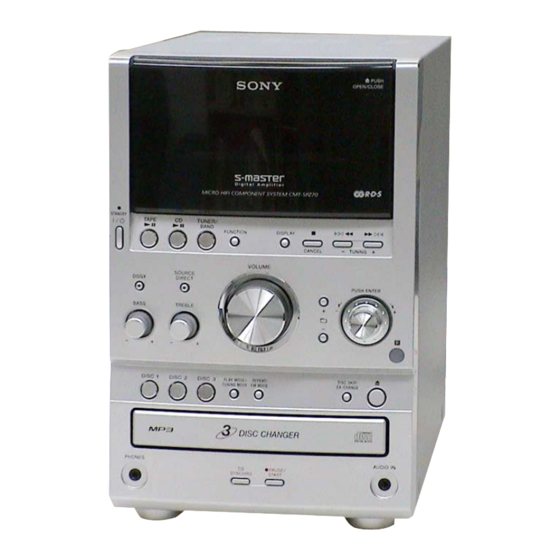
Photo: HCD-SPZ70
Model Name Using Similar Mechanism
CD Mechanism Name
Base Unit Name
Optical Pick-Up Block Name
Model Name Using Similar Mechanism
Q Q
Tape Transport Mechanism Name
3
6 7
1 3
1 5
SPECIFICATIONS
CD player section
System: Compact disc and digital audio system
Laser Diode Properties
Emission Duration: Continuous
Laser Output*: Less than 44.6µW
* This output is the value measurement at a distance of 200 mm from the
objective lens surface on the Optical Pick-up Block with 7mm aperture.
Frequency response: 20 Hz – 20 kHz (±2 dB)
Wavelength: 780 – 790 nm
Tape deck section
Recording system: 4-track 2-channel, stereo
Frequency response: 50 – 13,000 Hz (±3 dB), using Sony TYPE I cassettes
Tuner section
FM stereo, FM/AM superheterodyne tuner
FM tuner section:
Tuning range: 87.5 – 108.0 MHz
Antenna: FM lead antenna
Antenna terminals: 75 ohms unbalanced
Intermediate frequency: 10.7 MHz
AM tuner section:
Tuning range
European and Russian models: 531 – 1,602 kHz (with 9 kHz tuning interval)
Latin American model: 530 – 1,710 kHz (with 10 kHz tuning interval)
Other models: 530 – 1,710 kHz (with 10 kHz tuning interval)
531 – 1,602 kHz (with 9 kHz tuning interval)
Antenna: AM loop antenna
Antenna terminals: External antenna terminal
Intermediate frequency: 450 kHz
COMPACT DISC DECK RECEIVER
co
.
9 4
2 8
AEP Model
UK Model
HCD-SPZ50/SPZ70
Australian Model
NEW
DLM3A
BU-K6BD83S-WOD
KSM-213DCP
NEW
CFP42601
0 5
8
2 9
9 4
2 8
531 – 1,710 kHz (with 9 kHz tuning interval)
– Continued on next page –
m
9 9
E Model
HCD-SPZ50
9 9
Advertisement
Table of Contents


Need help?
Do you have a question about the HCD-SPZ50 and is the answer not in the manual?
Questions and answers