Table of Contents
Advertisement
SERVICE MANUAL
Ver. 1.0 2013.04
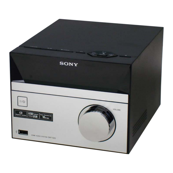
• HCD-S20 is compact disc receiver in CMT-S20.
Amplifier section
Power output (rated): 4 watts + 4 watts
(8 ohms at 1 kHz, 1% THD)
Continuous RMS power output (reference):
5 watts + 5 watts (8 ohms at 1 kHz, 10% THD)
Input
AUDIO IN (stereo mini jack): Sensitivity 1 V,
impedance 50 kilohms
Outputs
SPEAKERS: Accepts impedance of 8 ohms
CD player section
System: Compact disc and digital audio system
Laser Diode Properties
Emission Duration: Continuous
Laser Output*: Less than 44.6μW
* This output is the value measurement at a distance of
200mm from the objective lens surface on the Optical
Pick-up Block with 7mm aperture.
Frequency response: 20 Hz
Signal-to-noise ratio: More than 90 dB
Dynamic range: More than 90 dB
Tuner section
FM stereo, FM superheterodyne tuner
Antenna: FM lead antenna
Tuning range: 87.5 MHz
step)
USB section
(USB) port: Type A, maximum current 500 mA
9-893-739-01
Sony Corporation
2013D33-1
©
2013.04
Published by Sony Techno Create Corporation
Model Name Using Similar Mechanism
Mechanism Type
SPECIFICATIONS
Supported audio formats
Supported bit rate:
MP3 (MPEG 1 Audio Layer-3): 32 kbps
320 kbps, VBR
WMA: 32 kbps
Sampling frequencies:
MP3 (MPEG 1 Audio Layer-3): 32/44.1/48 kHz
WMA: 44.1 kHz
General
Except Korean model:
Power requirements: AC 120 V
Korean model:
Power requirements: AC 220 V
Power consumption: 18 watts
Dimensions (W/H/D, including largest
protrusions) (excl. speakers):
Approx. 170 mm × 133 mm × 240 mm
Mass (excl. speakers): Approx. 1.3 kg
20 kHz
Quantity of the main unit: 1 piece
Design and specifications are subject to change
without notice.
Standby power consumption: 0.5 W
108.0 MHz (50 kHz
Halogena ted flame retardants are not used in
the certain printed wiring boards.
HCD-S20
NEW
TDL-5
192 kbps, VBR
240 V, 50/60 Hz
240 V, 50/60 Hz
COMPACT DISC RECEIVER
E Model
Advertisement
Table of Contents

Related Manuals for Sony HCD-S20


Summary of Contents for Sony HCD-S20
- Page 1 HCD-S20 SERVICE MANUAL E Model Ver. 1.0 2013.04 • HCD-S20 is compact disc receiver in CMT-S20. Model Name Using Similar Mechanism Mechanism Type TDL-5 SPECIFICATIONS Amplifier section Supported audio formats Power output (rated): 4 watts + 4 watts Supported bit rate:...
-
Page 2: Table Of Contents
COMPONENTS IDENTIFIED BY MARK 0 OR DOTTED LINE WITH MARK 0 ON THE SCHEMATIC DIAGRAMS AND IN THE PARTS LIST ARE CRITICAL TO SAFE OPERATION. REPLACE THESE COMPONENTS WITH SONY PARTS WHOSE PART NUMBERS APPEAR AS SHOWN IN THIS MANUAL OR IN SUPPLEMENTS PUBLISHED BY SONY. -
Page 3: Servicing Notes
HCD-S20 SECTION 1 SERVICING NOTES RELEASING THE DISC TRAY LOCK NOTES ON HANDLING THE OPTICAL PICK-UP The disc tray lock function for the antitheft of sample disc in the BLOCK OR BASE UNIT shop is equipped. The laser diode in the optical pick-up block may suffer electro-... - Page 4 HCD-S20 MODEL IDENTIFICATION Distinguish by model number label stuck on the rear side of a main unit. MODEL NUMBER LABEL 110 – 240V AC area in E model (E32) Singapore model (SP1) 05/2013 Saudi Arabia model (EA3) Argentina model (AR2)
- Page 5 HCD-S20 COMPONENT REPAIR GUIDE 3. When You Plug Power Cord and Turn The Main Unit ON, The Main Unit Won’t Read Disc Normal 1. No Display When You Turn The Main Unit ON When you plug power cord and turn the main unit on, VFD won’t Procedure: display.
- Page 6 HCD-S20 HOW TO EJECT THE DISC WHEN POWER SWITCH TURN OFF 1 Refer to “SECTION 2. DISASSEMBLY” (page 7), remove the top cover assy S20 and the rear panel block from the unit. 3 Pull out the disc tray. top side 2 Turn the traverse gear in –...
-
Page 7: Disassembly
HCD-S20 SECTION 2 DISASSEMBLY • This set can be disassembled in the order shown below. 2-1. DISASSEMBLY FLOW 2-2. TOP COVER ASSY S20 (Page 7) 2-3. POWER CORD (AC1), REAR PANEL (Page 8) 2-4. CD DOOR (S20) (Page 8) 2-5. LOADER (TDL-5) & OPU ASSY (CDM1) (Page 9) 2-6. -
Page 8: Power Cord (Ac1), Rear Panel
HCD-S20 2-3. POWER CORD (AC1), REAR PANEL 3 Remove the rear panel block in the direction of an arrow. 6 rear panel top side 2 claw 2 claw bottom side 2 claw 4 power cord connector (CN503) 1 screw (3) 2 claw –... -
Page 9: Loader (Tdl-5) & Opu Assy (Cdm1)
HCD-S20 2-5. LOADER (TDL-5) & OPU ASSY (CDM1) Note 1: Before disconnecting the flexible flat cable of the loader (TDL-5) & OPU assy (CDM1), solder the short-land. 2 screws (3) 7 loader (TDL-5) & OPU assy Note 4: The wire is soldered to the (CDM1) terminal of the switch. -
Page 10: Vfd Board
HCD-S20 2-7. VFD BOARD 1 three claws Wire e i VFD board 2 VFD board – r re r ie – – r re r ie – 2-8. USB BOARD 4 six claws 1 VOL knob 5 USB board 2 screw (1) –... -
Page 11: Main Board
HCD-S20 2-9. MAIN BOARD ire e i Wire from USB board is upper. 1 connector (CON2) 5 screw (3) 6 MAIN board Wire from VFD board is lower. 4 connector – Rear view – (XP12) 2 connector 3 connector (XP6) -
Page 12: Test Mode
HCD-S20 SECTION 3 TEST MODE SOFTWARE VERSION TRAY LOCK It can confi rm the software version. It can be unable to take sample disc out of disc tray in the shop. Procedure: Procedure: 1. Press the [ ] button to turn the power on. -
Page 13: Electrical Check
HCD-S20 SECTION 4 ELECTRICAL CHECK CD SECTION Note: 1. CD block is basically constructed to operate without adjustment. 2. Use YEDS-18 disc (Part No. 3-702-101-01) unless otherwise indicat- 3. Use an oscilloscope with more than 10 M impedance. 4. Clean the object lens by an applicator with neutral detergent when the signal level is low than specifi... -
Page 14: Troubleshooting
HCD-S20 SECTION 5 TROUBLESHOOTING 1. Operation Check Flow Check if the voltage at pin 1 of CON2 on the Power is turned on. Exchange the POWER board. POWER board is +12V. Exchange the VFD and check if the power is Exchange the MAIN board. - Page 15 HCD-S20 2. Flow When “OVER CURRENT” is Displayed “OVER CURRENT” is Disconnect the USB board and check if the Exchange the USB board. displayed on the VFD. display persists. Exchange the MAIN board. 3. Flow When “PROTECT” is Displayed “PROTECT” is Check the if the voltage at pin 1 of CON2 on Exchange the POWER board.
-
Page 16: Diagrams
HCD-S20 SECTION 6 DIAGRAMS 6-1. BLOCK DIAGRAM POWER SDRAM FLASH CONTROL M12L64164 EN25T80 DATA USB005 OTHER LOADER TDM-5+IM OPU Moto driver IC MPEG Decoder 5W*2 CD5890 SPHE8104-MW STA339BWS 3.3V 1.2V AUX IN EAR004 AUDIO SW IC UART RZ5B705 74HC4052 IRR006... -
Page 17: Board Component Diagram (1/3)
HCD-S20 6-2. BOARD COMPONENT DIAGRAM (1/3) 8ohm 8ohm AUDIO IN TUNER TUNER L/R Out 74HC4053 ST339BWS AK5358 MAIN+AMP BOARD MOTER DRIVER 5890 FLASH IIS DATA OUT POWER_BOARD HOMESW SPHE8104MW INSW SDRAM M0516 PCF8563 4PIN/2.5mm 4PIN*2.0 12PIN/2.0 XP12 XS301 12PIN 4PIN*2.0 4PIN*2.0... -
Page 18: Board Component Diagram (2/3)
HCD-S20 6-3. BOARD COMPONENT DIAGRAM (2/3) Main Board PCB LAYOUT SPK2.0 Audio IN Tunner FM3.3V 74HC4052 3.3V AK5358 MOTER Motor Contr DRIVER 5890 FLASH Motor Contr I2S IN Signal I2S In Signal SPHE8104MW SDRAM STB3.3V M0516 +12V EUP3482A XP12 4PIN*2.0 12PIN*2.0... -
Page 19: Board Component Diagram (3/3)
HCD-S20 6-4. BOARD COMPONENT DIAGRAM (3/3) MCU3V3 LDO G9091 MCU_M516 15mA 0.5A VBUS SWITCH SWITCH MO_VCC 500mA MOTO DRIVER IC 5890 MCU GPIO 18mA ADC_AK5358A DC-DC 25mA DVCC3 FLASH 5890 74HC4052 50mA SRV33 +12V SDRAM POWER BOARD EUP3482A RFV33 MAX 2.3A... - Page 20 HCD-S20 THIS NOTE IS COMMON FOR PRINTED WIRING BOARDS AND SCHEMATIC DIAGRAMS. • Circuit Boards Location (In addition to this, the necessary note is printed in each block.) For Printed Wiring Boards. For Schematic Diagrams. POWER board Note: Note: • All capacitors are in μF unless otherwise noted. (p: pF) 50 •...
-
Page 21: Printed Wiring Board - Main Board
HCD-S20 6-5. PRINTED WIRING BOARD - MAIN Board - • See page 20 for Circuit Boards Location. • : Uses unleaded solder. MAIN BOARD (COMPONENT SIDE) MAIN BOARD (CONDUCTOR SIDE) HCD-S20... -
Page 22: Schematic Diagram - Main Board (1/6)
HCD-S20 6-6. SCHEMATIC DIAGRAM - MAIN Board (1/6) - MAIN BOARD (1/6) POWER_EN1 POWER_EN1 12V_IN BAT54S BAT54S From Power Board -24V VC12 VC12 R275 R275 POWER_EN2 POWER_EN2 C130 0.1uF/50V/X7R C130 0.1uF/50V/X7R 330pF/50V/X7R 330pF/50V/X7R 4PIN/2.5mm/40mm 4PIN/2.5mm/40mm 0.1uF/50V/X7R 0.1uF/50V/X7R 0.1uF/50V/X7R 0.1uF/50V/X7R 22uF/50V... -
Page 23: Schematic Diagram - Main Board (2/6)
HCD-S20 6-7. SCHEMATIC DIAGRAM - MAIN Board (2/6) - MAIN BOARD (2/6) Crystal 100K 100K 27MHz/30PPM 27MHz/30PPM UPG5V 33pF/50V/NP0 33pF/50V/NP0 33pF/50V/NP0 33pF/50V/NP0 RF3.3V Put these circuits as DVCC3 F3V3 F3V3 closer as possible to VCC1.2 4PIN/2.0mm 4PIN/2.0mm MPEG DECODER. VCC1.2 4.7uF/16V/Y5V... -
Page 24: Schematic Diagram - Main Board (3/6)
HCD-S20 6-8. SCHEMATIC DIAGRAM - MAIN Board (3/6) - MAIN BOARD (3/6) SDRAM SD33 MA10 DQ10 A10/AP DQ10 MA11 DQ11 DQ11 DBA0 DQ12 BA0/A13 DQ12 DBA1 DQ13 BA1/A12 DQ13 DQ14 DQ14 DQ[0..15] SDCLK DQ15 DRAS# RAS# DQ15 DQ[0..15] SD33 MA[0..11] SD33 MA[0..11]... -
Page 25: Schematic Diagram - Main Board (4/6)
HCD-S20 6-9. SCHEMATIC DIAGRAM - MAIN Board (4/6) - MAIN BOARD (4/6) DVCC3 MCU3V3 POWER_EN1 POWER_EN1 MCU3V3 RTC_3.3V POWER_EN2 POWER_EN2 AUDIO_MUTE AUDIO_MUTE RTC_3.3V LL4148 LL4148 R131 R131 POWER KEY MPEG_RST MPEG_RST RTC_3.3V R127 R127 VOL- MCU_RXD MCU_RXD VOL+ MCU_TXD R128... -
Page 26: Schematic Diagram - Main Board (5/6)
HCD-S20 6-10. SCHEMATIC DIAGRAM - MAIN Board (5/6) - MAIN BOARD (5/6) C153 NC/1uF/10V/Y5V C153 NC/1uF/10V/Y5V AD_BCLK 6,11 AD_BCLK AD_MCLK 6,11 AD_MCLK AD_LRCK 6,11 AD_LRCK AGND 12MHz 12MHz AD_DATA AD_DATA XP38 XP38 VDDRF FB14 FB14 4.7nh 4.7nh FRF1 GNDRF IISD... -
Page 27: Schematic Diagram - Main Board (6/6)
HCD-S20 6-11. SCHEMATIC DIAGRAM - MAIN Board (6/6) - MAIN BOARD (6/6) AMP_12V DVCC3 +3.3VD FB12 FB12 500/200mA 500/200mA FB28 FB28 300/2A 300/2A +3.3VD CE56 CE56 C221 C221 0.1uF/50V/X7R 0.1uF/50V/X7R 100uF/16V 100uF/16V C224 C224 VDD_DIG GND_SUB 0.1uF/50V/X7R 0.1uF/50V/X7R GND_DIG R274... -
Page 28: Printed Wiring Board - Usb Board
HCD-S20 6-12. PRINTED WIRING BOARD - USB Board - • See page 20 for Circuit Boards Location. • : Uses unleaded solder. USB BOARD (COMPONENT SIDE) USB BOARD (CONDUCTOR SIDE) HCD-S20... -
Page 29: Schematic Diagram - Usb Board
HCD-S20 6-13. SCHEMATIC DIAGRAM - USB Board - USB BOARD KEY_POWER 4PIN/2.0mm/100mm 4PIN/2.0mm/100mm KEY_POWER VOL- VOL+ SW14 SW14 TAC020 TAC020 100pF/50V/NP0 100pF/50V/NP0 4PIN/2mm 4PIN/2mm VOL- VOL- VOL+ VOL+ ENCODER ENCODER 4PIN/2.0mm/100mm 4PIN/2.0mm/100mm 100pF/50V/NP0 100pF/50V/NP0 100pF/50V/NP0 100pF/50V/NP0 1uF/25V/Y5V 1uF/25V/Y5V 0.1uF/25V/Y5V 0.1uF/25V/Y5V... -
Page 30: Printed Wiring Board - Vfd Board
HCD-S20 6-14. PRINTED WIRING BOARD - VFD Board - • See page 20 for Circuit Boards Location. • : Uses unleaded solder. VFD BOARD (COMPONENT SIDE) VFD BOARD (CONDUCTOR SIDE) HCD-S20... -
Page 31: Schematic Diagram - Vfd Board
HCD-S20 6-15. SCHEMATIC DIAGRAM - VFD Board - VFD BOARD +12V VFD135 VFD135 12PIN/2.0MM/220mm 12PIN/2.0MM/220mm +5VA VFD_CLK VFD_DATA +12VA VFD_CS NPN_3DG3904M NPN_3DG3904M +12V NPN_3DG3904M NPN_3DG3904M -24V 0.1uF/50V/X7R 0.1uF/50V/X7R 3.3uF/50V 3.3uF/50V 330/1% 330/1% IR_5V NPN_3DG3904M NPN_3DG3904M ADC_KEY2 4.7K 4.7K ADC_KEY1 PNP_3CG3906M... -
Page 32: Printed Wiring Board - Key Board
HCD-S20 6-16. PRINTED WIRING BOARD - KEY Board - • See page 20 for Circuit Boards Location. • : Uses unleaded solder. KEY BOARD (COMPONENT SIDE) KEY BOARD (CONDUCTOR SIDE) HCD-S20... -
Page 33: Schematic Diagram - Key Board
HCD-S20 6-17. SCHEMATIC DIAGRAM - KEY Board - KEY BOARD ADC_KEY1 ADC_KEY1 ADC_KEY2 ADC_KEY2 ESD11 ESD11 TUNE- TUNE- NC/PESD5V0S1BA/30K/35pF NC/PESD5V0S1BA/30K/35pF ESD12 ESD12 3PIN/2.0mm 3PIN/2.0mm 100pF/50V/NP0 100pF/50V/NP0 100pF/50V/NP0 100pF/50V/NP0 NC/PESD5V0S1BA/30K/35pF NC/PESD5V0S1BA/30K/35pF 2.2K 2.2K 2.2K 2.2K ENTER ENTER SW1:0V 6.8K/1% 6.8K/1% 6.8K/1% 6.8K/1%... -
Page 34: Schematic Diagram - Power Board
HCD-S20 6-18. SCHEMATIC DIAGRAM - POWER Board - POWER BOARD C501 C501 0.0022uF(222)400V 0.0022uF(222)400V R5051 R5051 R5052 R5052 R5053 R5053 R5054 R5054 D504 D504 D503 D503 150K 150K 150K 150K 150K 150K 150K 150K R509 R509 CE501 CE501 CE502 CE502... -
Page 35: Printed Wiring Board - Power Board
HCD-S20 6-19. PRINTED WIRING BOARD - POWER Board - • See page 20 for Circuit Boards Location. • : Uses unleaded solder. POWER BOARD POWER BOARD (COMPONENT SIDE) (CONDUCTOR SIDE) -
Page 36: Exploded Views
HCD-S20 SECTION 7 EXPLODED VIEWS Note: • -XX and -X mean standardized parts, so • Color Indication of Appearance Parts Ex- The components identifi ed by mark 0 they may have some difference from the ample: or dotted line with mark 0 are critical for original one. -
Page 37: Chassis Section
HCD-S20 7-2. CHASSIS SECTION CDM1 ACP1 (E32) not supplied front panel section not supplied supplied not supplied not supplied Ref. No. Part No. Description Remark Ref. No. Part No. Description Remark A-1945-220-A MAIN BOARD, COMPLETE 0 AC1 9-885-185-55 CORD, POWER (EA) -
Page 38: Front Panel Section
HCD-S20 7-3. FRONT PANEL SECTION supplied Ref. No. Part No. Description Remark Ref. No. Part No. Description Remark 4-465-831-01 VOL KNOB 4-465-832-01 SCREW (1) X-2587-412-1 FRONT PANEL ASSY S20 A-1945-218-A VFD BOARD, COMPLETE A-1945-217-A USB BOARD, COMPLETE (Including KEY board) - Page 39 HCD-S20 MEMO...
- Page 40 HCD-S20 REVISION HISTORY Ver. Date Description of Revision 2013.04...
Need help?
Do you have a question about the HCD-S20 and is the answer not in the manual?
Questions and answers