Table of Contents
Advertisement
SERVICE MANUAL
Sec. 1: Main Section
I Specifications
I Preparation for Servicing
I Adjustment Procedures
I Schematic Diagrams
I CBA's
I Exploded views
I Parts List
VIDEO CASSETTE RECORDER
DVD PLAYER &
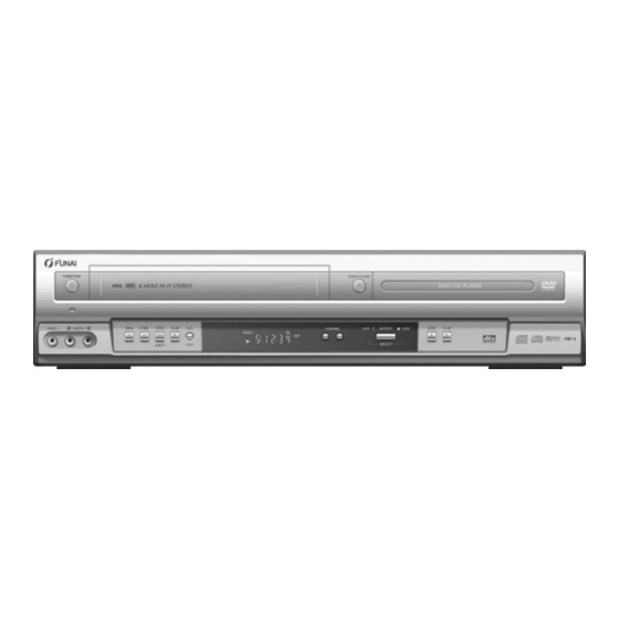
DPVR-5505
DPVR-5505V
DPVR-5805
Sec. 2: Deck Mechanism Section
I Standard Maintenance
I Alignment for Mechanism
I Disassembly/Assembly of Mechanism
I Alignment Procedures of Mechanism
I Deck Exploded Views
I Deck Parts List
PAL
Advertisement
Chapters
Table of Contents

Subscribe to Our Youtube Channel
Related Manuals for FUNAI DPVR-5505


Summary of Contents for FUNAI DPVR-5505
-
Page 1: Dvd Player
I Adjustment Procedures I Disassembly/Assembly of Mechanism I Schematic Diagrams I Alignment Procedures of Mechanism I CBA’s I Deck Exploded Views I Exploded views I Deck Parts List I Parts List DVD PLAYER & VIDEO CASSETTE RECORDER DPVR-5505 DPVR-5505V DPVR-5805... -
Page 2: Table Of Contents
MAIN SECTION DVD PLAYER & VIDEO CASSETTE RECORDER DPVR-5505/DPVR-5505V /DPVR-5805 Sec. 1: Main Section I Specifications I Preparation for Servicing I Adjustment Procedures I Schematic Diagrams I CBA’s I Exploded Views I Parts List TABLE OF CONTENTS Specifications ............... . . 1-1-1 Laser Beam Safety Precautions . -
Page 3: Specifications
SPECIFICATIONS < VCR Section > Description Unit Minimum Nominal Maximum Remark 1. Video 1-1. Video Output (PB) Vp-p SP Mode 1-2. Video Output (R/P) Vp-p SP Mode, 1-3. Video S/N Y (R/P) W/O Burst 1-4. Video Color S/N AM (R/P) SP Mode 1-5. -
Page 4: Dvd Section
< DVD Section > ITEM CONDITIONS UNIT NOMINAL LIMIT 1. Video Output 75 ohm load ± 0.1 2. Optical Digital Out 3. Audio (PCM) 3-1. Output Level 1 kHz 0 dB Vrms 3-2. S/N 3-3. Freq. Response fs = 48 kHz ± 0.5dB 20~22 k fs = 44.1 kHz ±... -
Page 5: Laser Beam Safety Precautions
LASER BEAM SAFETY PRECAUTIONS This DVD player uses a pickup that emits a laser beam. Do not look directly at the laser beam coming from the pickup or allow it to strike against your skin. The laser beam is emitted from the location shown in the figure. When checking the laser diode, be sure to keep your eyes at least 30cm away from the pickup lens when the diode is turned on. -
Page 6: Important Safety Precautions
IMPORTANT SAFETY PRECAUTIONS Product Safety Notice J. Be careful that foreign objects (screws, solder droplets, etc.) do not remain inside the set. Some electrical and mechanical parts have special K. Crimp type wire connector safety-related characteristics which are often not evi- The power transformer uses crimp type connectors dent from visual inspection, nor can the protection they which connect the power cord and the primary side... -
Page 7: Safety Check After Servicing
Safety Check after Servicing Examine the area surrounding the repaired location for Chassis or Secondary Conductor damage or deterioration. Observe that screws, parts, and wires have been returned to their original posi- Primary Circuit Terminals tions. Afterwards, do the following tests and confirm the specified values to verify compliance with safety standards. -
Page 8: Standard Notes For Servicing
STANDARD NOTES FOR SERVICING Circuit Board Indications Pb (Lead) Free Solder When soldering, be sure to use the Pb free solder. 1. The output pin of the 3 pin Regulator ICs is indi- cated as shown. How to Remove / Install Flat Pack-IC Top View Bottom View 1. - Page 9 3. The flat pack-IC on the CBA is affixed with glue, so With Soldering Iron: be careful not to break or damage the foil of each (1) Using desoldering braid, remove the solder from all pin or the solder lands under the IC when removing pins of the flat pack-IC.
- Page 10 (4) Bottom of the flat pack-IC is fixed with glue to the 2. Installation CBA; when removing entire flat pack-IC, first apply (1) Using desoldering braid, remove the solder from soldering iron to center of the flat pack-IC and heat the foil of each pin of the flat pack-IC on the CBA so up.
- Page 11 Instructions for Handling Semi-conductors Electrostatic breakdown of the semi-conductors may occur due to a potential difference caused by electro- static charge during unpacking or repair work. 1. Ground for Human Body Be sure to wear a grounding band (1MΩ) that is prop- erly grounded to remove any static electricity that may be charged on the body.
-
Page 12: Preparation For Servicing
PREPARATION FOR SERVICING How to Enter the Service Mode About Optical Sensors Caution: An optical sensor system is used for the Tape Start and End Sensors on this equipment. Carefully read and follow the instructions below. Otherwise the unit may operate erratically. What to do for preparation Insert a tape into the Deck Mechanism Assembly and press the PLAY button. -
Page 13: Disassembly Method
CABINET DISASSEMBLY INSTRUCTIONS 1. Disassembly Flowchart REMOVAL This flowchart indicates the disassembly steps to gain REMOVE/*UNHOOK/ LOC. PART Fig. access to item(s) to be serviced. When reassembling, UNLOCK/RELEASE/ Note follow the steps in reverse order. Bend, route, and UNPLUG/DESOLDER dress the cables as they were originally. Loader 2(S-6) [1] Top Case... - Page 14 Reference Notes CAUTION 1: Locking Tabs (L-1) and (L-2) are fragile. Be careful not to break them. (S-1) (S-1) 1-1. Release three Locking Tabs (L-1). [1] Top Case 1-2. Release three Locking Tabs (L-2), then remove the Front Assembly. CAUTION 2: Electrostatic breakdown of the laser (S-1) diode in the optical system block may occur as a potential difference caused by electrostatic charge...
- Page 15 CN401 (S-3) CN601 (S-9) (S-8) (S-3) (S-8) [4] DVD Mecha (S-9) Assembly (S-3) (S-4) [5] Partition Plate (S-8) (S-10) (S-5) (S-6) CN501 (S-10) [9] VCR Chassis Unit [7] Loader Holder [6] Power Supply CBA (L-3) Fig. D5 Fig. D3 (S-7) (S-7) [8] DVD Main CBA CN301...
- Page 16 Cylinder Assembly FE Head ACE Head Assembly [10] Deck Assembly SW507 Lead with blue stripe Lead with blue stripe LD-SW Desolder [14] Jack-A CBA (S-11) (S-13) [13] Main CBA [10] Deck Assembly [12] Power SW CBA Cam Gear [13] Main CBA Desolder (S-11) Hole...
- Page 17 HOW TO EJECT MANUALLY 1. Remove the Top Case. 2. Rotate the roulette in the direction of the arrow as shown below. 3. Pull the tray slowly with a hand. View for A Rotate this roulette in the direction of the arrow DVD Mecha 1-6-5 H9773DC...
-
Page 18: Electrical Adjustment Instructions
ELECTRICAL ADJUSTMENT INSTRUCTIONS General Note: "CBA" is an abbreviation for "Circuit Board Assembly." NOTE: Figure 1 1.Electrical adjustments are required after replacing circuit components and certain mechanical parts. It is important to do these adjustments only after all repairs and replacements have been com- EXT. -
Page 19: Firmware Renewal Mode
FIRMWARE RENEWAL MODE 1. Turn the power on and remove the disc on the tray. 5. After programming is finished, the tray opens auto- 2. To put the DVD player into version up mode, press matically. Fig. e appears on the screen and the [9], [8], [7], [6], and [SEARCH MODE] buttons on checksum in (*2) of Fig. -
Page 20: Block Diagrams
BLOCK DIAGRAMS <VCR SECTION> Servo/System Control Block Diagram 1-9-1 H9776BLS... - Page 21 Video Block Diagram 1-9-2 H9776BLV...
- Page 22 Audio Block Diagram ( A, B ) 1-9-3 H9776BLA...
- Page 23 Audio Block Diagram ( C ) H9778BLA 1-9-4...
- Page 24 Hi-Fi Audio Block Diagram ( C ) 1-9-5 H9778BLH...
- Page 25 Power Supply Block Diagram 1-9-6 H9776BLP...
- Page 26 BLOCK DIAGRAMS <DVD SECTION> DVD System Control / Servo Block Diagram H9776BLSD 1-9-7...
- Page 27 Digital Signal Process Block Diagram H9776BLD 1-9-8...
- Page 28 DVD Video / Audio Block Diagram H9776BLVD 1-9-9...
-
Page 29: Function Indicator Symbols
FUNCTION INDICATOR SYMBOLS Note: If a mechanical malfunction occurs, the power is turned off. When the power comes on again after that by pressing [FUNCTION] button, an error message is displayed on the TV screen for 5 seconds. MODE INDICATOR ACTIVE When reel or capstan mechanism is not “A R”... -
Page 30: Schematic Diagrams / Cba's And Test Points
SCHEMATIC DIAGRAMS / CBA’S AND TEST POINTS Standard Notes WARNING Many electrical and mechanical parts in this chassis have special characteristics. These characteristics often pass unnoticed and the protection afforded by them cannot necessarily be obtained by using replace- ment components rated for higher voltage, wattage, etc. - Page 31 LIST OF CAUTION, NOTES, AND SYMBOLS USED IN THE SCHEMATIC DIAGRAMS ON THE FOLLOWING PAGES: 1. CAUTION: FOR CONTINUED PROTECTION AGAINST FIRE HAZARD, REPLACE ONLY WITH THE SAME TYPE FUSE. 2. CAUTION: Fixed Voltage (or Auto voltage selectable) power supply circuit is used in this unit. If Main Fuse (F1001) is blown, first check to see that all components in the power supply circuit are not defective before you connect the AC plug to the AC power supply.
- Page 32 Main 1/8 Schematic Diagram < VCR Section > Comparison Chart of Models and Marks MODEL MARK DPVR-5505 DPVR-5505V DPVR-5805 1-10-4 1-10-3 H9776SCM1...
- Page 33 Main 2/8, Sensor & Power SW Schematic Diagrams < VCR Section > IC611 MATRIX CHART SACD PSCAN REPEAT SACD GROUP REPEAT TITLE GROUP PSCAN TITLE HD VCD Comparison Chart of Models and Marks MODEL MARK DPVR-5505 DPVR-5505V DPVR-5805 1-10-6 1-10-5 H9776SCM2...
- Page 34 Main 3/8 Schematic Diagram < VCR Section > Comparison Chart of Models and Marks MODEL MARK DPVR-5505 DPVR-5505V DPVR-5805 1-10-7 1-10-8 H9776SCM3...
- Page 35 Main 4/8 Schematic Diagram < VCR Section > H9776SCM4 1-10-9 1-10-10...
- Page 36 Main 5/8 Schematic Diagram < VCR Section > Comparison Chart of Models and Marks MODEL MARK DPVR-5505 DPVR-5505V DPVR-5805 1-10-11 1-10-12 H9776SCM5...
- Page 37 Main 6/8 Schematic Diagram < VCR Section > Comparison Chart of Models and Marks MODEL MARK DPVR-5505 DPVR-5505V DPVR-5805 1-10-13 1-10-14 H9776SCM6...
- Page 38 Main 7/8 & DVD Open/Close Schematic Diagrams < VCR Section > PIN NAME (*1~*4) CHART MODEL A, B MARK PLAY FP-CLK SKIP-DOWN FP-DIN DISC-IN FP-STB SKIP-UP FP-DOUT PIN NAME MAY DIFFER BY MODELS. Comparison Chart of Models and Marks MODEL MARK DPVR-5505 DPVR-5505V DPVR-5805 1-10-15 1-10-16 H9776SCM7...
- Page 39 Main 8/8 Schematic Diagram ( C ) < VCR Section > Comparison Chart of Models and Marks MODEL MARK DPVR-5505 DPVR-5505V DPVR-5805 1-10-17 1-10-18 H9778SCM8...
- Page 40 For continued protection against fire hazard, The voltage for parts in hot circuit is measured using DPVR-5505 If Main Fuse (F1001) is blown, check to see that all components in the power supply replace only with the same type fuse.
- Page 41 Jack-A Schematic Diagram < VCR Section > Comparison Chart of Models and Marks MODEL MARK DPVR-5505 DPVR-5505V DPVR-5805 1-10-21 1-10-22 H9776SCJ...
- Page 42 AFV Schematic Diagram ( C ) < VCR Section > Comparison Chart of Models and Marks MODEL MARK DPVR-5505 DPVR-5505V DPVR-5805 1-10-23 1-10-24 H9778SCAFV...
- Page 43 Main CBA & Sensor CBA Top View Sensor CBA Top View BHF300F01011A TP751 TP301 BHF300F01011B V-OUT C-PB VR501 SW-P TP504 RF-SW TP501 S-INH TP503 1-10-25 1-10-26 BH9700F01016A...
- Page 44 Main CBA Bottom View PIN 6 OF IC1403 PIN 19 OF CN1601 PIN 16 OF CN1601 PIN 14 OF CN1601 PIN 10 OF CN1601 PIN 1 OF CN1601 1-10-27 1-10-28 BH9700F01016A...
- Page 45 Power SW CBA Top View Power SW CBA Bottom View BH9700F01016B DVD Open/Close DVD Open /Close CBA Top View CBA Bottom View BH9700F01016C 1-10-30 1-10-29...
- Page 46 Jack-A CBA Top View Jack-A CBA Bottom View BH9700F01022C Comparison Chart of AFV CBA Top View ( C ) AFV CBA Bottom View ( C ) Models and Marks MODEL MARK DPVR-5505 DPVR-5505V DPVR-5805 BHC400F01093 1-10-32 1-10-31...
- Page 47 Power Supply CBA Top View Power Supply CBA Bottom View BECAUSE A HOT CHASSIS GROUND IS PRESENT IN THE POWER CAUTION ! CAUTION ! SUPPLY CIRCUIT , AN ISOLATION TRANSFORMER MUST BE USED. For continued protection against fire hazard, Fixed voltage ( or Auto voltage selectable ) power supply circuit is used in this unit. ALSO , IN ORDER TO HAVE THE ABILITY TO INCREASE THE INPUT replace only with the same type fuse.
- Page 48 DVD Main 1/3 Schematic Diagram < DVD Section > PIN NAME (*1~*4) CHART MODEL A, B MARK PLAY FP-CLK SKIP-DOWN FP-DIN DISC-IN FP-STB SKIP-UP FP-DOUT PIN NAME MAY DIFFER BY MODELS. Comparison Chart of Models and Marks MODEL MARK DPVR-5505 DPVR-5505V DPVR-5805 1-10-35 1-10-36 H9776SCD1...
- Page 49 DVD Main 2/3 Schematic Diagram < DVD Section > PIN NAME (*1~*4) CHART MODEL A, B MARK PLAY FP-CLK SKIP-DOWN FP-DIN DISC-IN FP-STB SKIP-UP FP-DOUT PIN NAME MAY DIFFER BY MODELS. Comparison Chart of Models and Marks MODEL MARK DPVR-5505 DPVR-5505V DPVR-5805 1-10-37 1-10-38 H9776SCD2...
- Page 50 Comparison Chart of Models and Marks MODEL MARK DPVR-5505 DPVR-5505V DPVR-5805 IC101 VOLTAGE CHART PIN.NO PLAY STOP PIN.NO PLAY STOP PIN.NO PLAY STOP PIN.NO PLAY STOP PIN.NO PLAY STOP PIN.NO PLAY STOP PIN.NO PLAY STOP PIN.NO PLAY STOP ----- -----...
- Page 51 DVD Main 3/3 Schematic Diagram < DVD Section > 1-10-41 1-10-42 H9776SCD3...
-
Page 52: Waveforms
WAVEFORMS NOTE: Input VCR: COLOR BAR SIGNAL (WF1~WF3) DVD: POWER ON (STOP) MODE (WF4~WF6) CD: 1kHz PLAY (WF7~WF9) TP301 UPPER TP504 Pin 1 of CN1601 Pin 14 of CN1601 LOWER C-PB 10mV x 10 RF-SW 0.5V x 10 VIDEO-Y VIDEO-Y 0.2V 0.2V 20µs... -
Page 53: Wiring Diagram < Vcr Section
WIRING DIAGRAM < VCR SECTION > 1-12-1 H9776WI... -
Page 54: Wiring Diagram < Dvd Section
WIRING DIAGRAM < DVD SECTION > H9776WID 1-12-2... -
Page 55: Ic Pin Function Descriptions
Function Name Level Comparison Chart of Models and Marks Color Phase Rotary Model Mark OUT C-ROTA Changeover SIgnal DPVR-5505 Video Head DPVR-5505V OUT H-A-SW Amp Switching DPVR-5805 Pulse Head Amp IN H-A- Comparator IC501( SERVO / SYSTEM CONTROL IC ) - Page 56 Signal Active Signal Active Mark Function Mark Function Name Level Name Level OUT D-REC-H Delayed Control Record Signal SCART 1 8Pin OUT 8POUT-2 Hi-z/L Level by using System Reset 8POUT-1 and IN RESET Signal 8POUT-2 (Reset=”L”) Not Used IN XCin Sub Clock A,B OUT AUDIO- Audio IN/OUT...
- Page 57 IC612 ( FIP DRIVER ) Signal Active Mark Function Name Level [ DPVR-5805 ] Take Up Reel IN T-REEL Rotation PULSE Signal Name Function Signal Name H/L/ OUT LM-FWD/ Loading Motor FP-CLK Clock Input Control Signal Hi-z OUT OUTPUT- FP-STB Serial Interface Strobe Output Select SELECT...
-
Page 58: Lead Identifications
LEAD IDENTIFICATIONS PQ070XZ5MZP MID-32A22F 2SA1175(F,H,J) 2SA1015-GR(TPE2) PT204-6B-12 2SC2785(F,H,J) 2SA1020(Y) BA1F4M-T 2SC1815-BL(TPE2) 1: Vin BN1F4M-T 2SC1815-GR(TPE2) 2: Vc BN1L4M-T 2SC1815-Y(TPE2) 3: Vo KRA103M 2SC2120-Y(TPE2) 4: Vadj KRC103M 2SC3266-Y(TPE2) 5: GND KTA1267(GR,Y) KTA1266(GR) 1 2 3 KTC3199(BL,GR,Y) KTA1281(Y) RN2204(TE4,T) KTC3203(Y) KTC3205(Y) E C B E C B 2SK3566 KIA4558P... -
Page 59: Exploded Views
2L051 2B54 2L012 2B46 2L020 2B13 JW007 2L054 2B15 2L053 JW009 2B15 2B16 2L020 2B15 2L020 [ DPVR-5505 2L051 2L011 JW008 /DPVR-5505V ] Junction CBA 2B33 2L012 2L054 JW006 Power Supply CBA 2B15 2L051 JW002 [ DPVR-5505 DVD Open/Close CBA... - Page 60 Packing Some Ref. Numbers are not in sequence. [ DPVR-5505 ] [ DPVR-5505V/DPVR-5805 ] X20A X20B X20C X20D Unit 1-15-3 H9776PEX...
-
Page 61: Mechanical Parts List
DRY BATTERY R6P/2S or XB0M451T0001 Comparison Chart of Models and Marks DRY BATTERY ES-GR6M-C XB0M571GLP01 Model Mark RF CORD PAL 1.2M or WPZ0122LG001 DPVR-5505 RF CABLE CC1001020012010 WPZ0122LW001 DPVR-5505V ACCESSORY BAG K8092BA 0VM404632 DPVR-5805 21P CABLE(BYR SUPPLY) H9300ED 0VMN03276 SERVICE CENTER LIST HC2C0ED... -
Page 62: Electrical Parts List
CHIP CERAMIC CAP .(1608) F Z 0.1µF/ CHD1EZ30F104 25V or Model Mark CHIP CERAMIC CAP . FZ Z 0.1µF/50V CHD1JZ3FZ104 DPVR-5505 C114 CHIP CERAMIC CAP .(1608) B K 1000pF/ CHD1JK30B102 DPVR-5505V DPVR-5805 C116 CHIP CERAMIC CAP . B K 2200pF/50V... - Page 63 Ref. No. Mark Description Part No. Ref. No. Mark Description Part No. CHIP CERAMIC CAP .(1608) F Z 0.1µF/ CHD1EZ30F104 CHIP CERAMIC CAP .(1608) B K 0.047µF/ CHD1EK30B473 25V or CHIP CERAMIC CAP . FZ Z 0.1µF/50V CHD1JZ3FZ104 C316 ELECTROLYTIC CAP . 1µF/50V M H7 CE1JMAVSL1R0 C153 CHIP CERAMIC CAP .(1608) F Z 0.1µF/...
- Page 64 Ref. No. Mark Description Part No. Ref. No. Mark Description Part No. C344 ELECTROLYTIC CAP . 4.7µF/25V M NP CP1EMAVSB4R7 CHIP CERAMIC CAP . CG J 68pF/50V CHD1JJ3CG680 C451 CHIP CERAMIC CAP .(1608) F Z 0.1µF/ CHD1JZ30F104 C345 ELECTROLYTIC CAP . 0.47µF/50V M H7 CE1JMAVSLR47 50V or C346...
- Page 65 Ref. No. Mark Description Part No. Ref. No. Mark Description Part No. C479 ELECTROLYTIC CAP . 10µF/16V M H7 CE1CMAVSL100 CHIP CERAMIC CAP .(1608) B K 0.047µF/ CHD1EK30B473 C480 ELECTROLYTIC CAP . 4.7µF/25V M H7 CE1EMAVSL4R7 C534 ELECTROLYTIC CAP . 47µF/6.3V M H7 CE0KMAVSL470 C481 ELECTROLYTIC CAP .
- Page 66 Ref. No. Mark Description Part No. Ref. No. Mark Description Part No. C711 CHIP CERAMIC CAP .(1608) B K 0.01µF/ CHD1JK30B103 CHIP CERAMIC CAP .(1608) F Z 0.1µF/ CHD1EZ30F104 25V or C712 CHIP CERAMIC CAP .(1608) F Z 0.1µF/ CHD1JZ30F104 CHIP CERAMIC CAP .
- Page 67 Ref. No. Mark Description Part No. Ref. No. Mark Description Part No. D054 ZENER DIODE DZ-10BSBT265 or NDTB00DZ10BS RECTIFIER DIODE 1N4005 NDWZ001N4005 ZENER DIODE MTZJT-7710B QDTB00MTZJ10 D1054 RECTIFIER DIODE 1N4005 or NDQZ001N4005 D056 ZENER DIODE DZ-18BSBT265 or NDTB00DZ18BS RECTIFIER DIODE 1N4005 NDWZ001N4005 ZENER DIODE MTZJT-7718B QDTB00MTZJ18...
- Page 68 Ref. No. Mark Description Part No. Ref. No. Mark Description Part No. L1251 INDUCTOR(0.47µH K) LAP02TAR47K LLAXKATTUR47 Q403 TRANSISTOR KTC3203(Y) or NQSY0KTC3203 L1351 INDUCTOR(100µH K) LAP02TA101K LLAXKATTU101 TRANSISTOR 2SC2120-Y(TPE2) QQSY02SC2120 L1521 CHOKE COIL 47µH-K or LLBD00PKV007 Q404 TRANSISTOR KTA1266(GR) or NQS40KTA1266 CHOKE COIL 47µH-K or LLBD00PKV005...
- Page 69 Ref. No. Mark Description Part No. Ref. No. Mark Description Part No. CARBON RES. 1/4W J 1.2k Ω TRANSISTOR 2SC2785(F) or QQSF02SC2785 R060 RCX4JATZ0122 CARBON RES. 1/4W J 8.2k Ω TRANSISTOR 2SC1815-Y(TPE2) or QQSY02SC1815 R061 RCX4JATZ0822 CHIP RES.(1608) 1/10W J 180 Ω TRANSISTOR 2SC1815-GR(TPE2) QQS102SC1815 R062...
- Page 70 Ref. No. Mark Description Part No. Ref. No. Mark Description Part No. CARBON RES. 1/6W J 33 Ω or CHIP RES.(1608) 1/10W J 39k Ω R307 RCX6JATZ0330 R452 RRXAJR5Z0393 CARBON RES. 1/4W J 33 Ω CHIP RES.(1608) 1/10W J 5.6k Ω RCX4JATZ0330 R453 RRXAJR5Z0562...
- Page 71 Ref. No. Mark Description Part No. Ref. No. Mark Description Part No. CARBON RES. 1/4W G 4.7k Ω CHIP RES.(1608) 1/10W J 10k Ω RCX4GATZ0472 R624 RRXAJR5Z0103 CHIP RES.(1608) 1/10W J 3.9k Ω CARBON RES. 1/6W J 1.8k Ω or R529 RRXAJR5Z0392 R703...
- Page 72 Ref. No. Mark Description Part No. Ref. No. Mark Description Part No. CHIP RES.(1608) 1/10W J 470 Ω R1223 RRXAJR5Z0471 TACT SWITCH TC-1104(H=9.5) SST0101DNG01 CHIP RES.(1608) 1/10W J 470 Ω R1224 RRXAJR5Z0471 SW506 LEAF SWITCH MXS01830MVP0 SSC0101MCE03 CHIP RES.(1608) 1/10W J 220 Ω R1227 RRXAJR5Z0221 SW507...
- Page 73 Ref. No. Mark Description Part No. Ref. No. Mark Description Part No. X'TAL 4.433619MHz 1811388 C017 ELECTROLYTIC CAP . 1000µF/16V M CE1CMZPTL102 X501 X'TAL 12.000MHz FXD126LDS001 C018 ELECTROLYTIC CAP . 470µF/6.3V M or CE0KMASDL471 X502 X'TAL 32.768kHz(20PPM) or FXC323LQUA01 ELECTROLYTIC CAP . 470µF/6.3V M CE0KMASTL471 X'TAL 32.768kHz(20PPM) FXC323LDS002...
- Page 74 Ref. No. Mark Description Part No. Ref. No. Mark Description Part No. RECTIFIER DIODE 1N4005 NDWZ001N4005 TRANSISTORS D1003 RECTIFIER DIODE 1N4005 or NDQZ001N4005 Q1001! FET 2SK3566 QFWZ02SK3566 RECTIFIER DIODE 1N4005 NDWZ001N4005 Q1003 TRANSISTOR 2SC1815-GR(TPE2) QQS102SC1815 D1004 RECTIFIER DIODE 1N4005 or NDQZ001N4005 Q1004 TRANSISTOR KTA1267(GR) or...
- Page 75 Ref. No. Mark Description Part No. Ref. No. Mark Description Part No. METAL OXIDE FILM RES. 1W J 2.7 Ω or R1043 RN012R7ZU001 COIL METAL OXIDE FILM RES. 1W J 2.7 Ω or RN012R7KE009 L102 BEAD CORE B16 RH 3.5X10X1.3 XL03010XM001 METAL OXIDE FILM RES.
- Page 76 Ref. No. Mark Description Part No. CHIP CERAMIC CAP .(1608) F Z 0.1µF/ CHD1EZ30F104 25V or CHIP CERAMIC CAP . FZ Z 0.1µF/50V CHD1JZ3FZ104 ELECTROLYTIC CAP . 3.3µF/50V M H7 CE1JMASSL3R3 CHIP CERAMIC CAP .(1608) F Z 0.1µF/ CHD1JZ30F104 50V or CHIP CERAMIC CAP .(1608) F Z 0.1µF/ CHD1EZ30F104 25V or...
- Page 77 DECK MECHANISM SECTION DVD PLAYER & VIDEO CASSETTE RECORDER DPVR-5505/DPVR-5505V /DPVR-5805 Sec. 2: Deck Mechanism Section I Standard Maintenance I Mechanism Alignment Procedures I Disassembly / Assembly of Mechanism I Deck Exploded Views I Deck Parts List TABLE OF CONTENTS Standard Maintenance .
-
Page 78: Standard Maintenance
STANDARD MAINTENANCE Service Schedule of Components This maintenance chart shows you the standard of replacement and cleaning time for each part. Because those may replace depending on environment and purpose for use, use the chart for reference. h: Hours : Cleaning I: Replace Deck Periodic Service Schedule... - Page 79 Cleaning Cleaning of ACE Head Clean the head with a cotton swab. Cleaning of Video Head Procedure Clean the head with a head cleaning stick or chamois 1.Remove the top cabinet. cloth. 2.Dip the cotton swab in 90% isopropyl alcohol and Procedure clean the ACE Head.
-
Page 80: Service Fixture And Tools
SERVICE FIXTURE AND TOOLS J-1-1, J-1-2 Ref. No. Name Part No. Adjustment J-1-1 Alignment Tape FL6A Head Adjustment of ACE Head J-1-2 Alignment Tape FL6N8 Azimuth and X Value Adjustment of ACE Head / (2 Head model) Adjustment of Envelope Waveform FL6NS8 (4 Head model) Guide Roller Adj. -
Page 81: Mechanical Alignment Procedures
MECHANICAL ALIGNMENT PROCEDURES Explanation of alignment for the tape to correctly run B. Method to place the Cassette Holder in the tape- starts on the next page. Refer to the information below loaded position without a cassette tape on this page if a tape gets stuck, for example, in the 1. -
Page 82: Tape Interchangeability Alignment
1. Tape Interchangeability Alignment Note: To do these alignment procedures, make sure that the Tracking Control Circuit is set to the preset position every time a tape is loaded or unloaded. (Refer to page 2-3-4, procedure 1-C, step 2.) Equipment required: Dual Trace Oscilloscope VHS Alignment Tape (FL6NS8) Guide Roller Adj. - Page 83 1-A. Preliminary/Final Checking and 4. If creasing or snaking is apparent, adjust the Tilt Alignment of Tape Path Adj. Screw of the ACE Head. (Fig. M6) Purpose: To make sure that the tape path is well stabilized. Azimuth Adj. Screw Symptom of Misalignment: If the tape path is unstable, the tape will be damaged.
- Page 84 5. To shift the CTL waveform, press CH UP or CH 5. When Guide Rollers [2] and [3] (Refer to Fig. M3) DOWN button on the remote control unit. Then are aligned properly, there is no envelope drop make sure that the maximum output position of PB either at the beginning or end of track as shown in ±...
- Page 85 1-D. Azimuth Alignment of Audio/Con- 2. When the tape has been curled up or bent, turn the trol/ Erase Head alignment screw to adjust the height of REV Post. (Refer to Fig. M11 and M13.) Purpose: To correct the Azimuth alignment so that the Audio/ Control/Erase Head meets tape tracks properly.
-
Page 86: Disassembly/Assembly Procedures Of Deck Mechanism
DISASSEMBLY/ASSEMBLY PROCEDURES OF DECK MECHANISM Before following the procedures described below, be sure to remove the deck assembly from the cabinet. (Refer to CABINET DISASSEMBLY INSTRUCTIONS.) All the following procedures, including those for adjustment and replacement of parts, should be done in Eject mode;... - Page 87 REMOVAL INSTALLATION STEP START- REMOVE/*UNHOOK/ /LOC. PART ADJUSTMENT Fig. No. UNLOCK/RELEASE/ CONDITION UNPLUG/DESOLDER BT Arm DM2H, DM14H *(P-5) [33] [26] Loading Arm (SP) (+)Refer to Alignment [34] [26] DM2H, DM14H Assembly Sec.Page 2-5-1 Loading Arm (TU) (+)Refer to Alignment [35] [34] DM2H, DM14H Assembly...
-
Page 88: Top View
Top View [44] [45] [49] [46] [14] [13] [11] [15] [38] [10] [12] [37] [36] [43] [32] [41] [31] [40] [42] Fig. DM1H Bottom View [19] [35] [34] [25] [23] [24] [26] [27] [22] [28] [20] [33] Fig. DM2H 2-4-3 U29PHSDA... - Page 89 (S-1) (S-1) (L-1) (L-3) (L-2) (S-1A) (P-1) Installation of [3] and [6] First, insert [6] diagonally in [3] as shown below. Then, install [6] in [3] while pushing (L-1) in a direction of arrow. After installing [6] in [3], confirm that pin A of [3] enters hole A of [6] properly.
- Page 90 [11] (S-4A) (L-4) [49] (P-3) [13] [50] Removal of [11] [12] (L-12) 1) Remove screw (S-4A). 2) Unhook spring (P-2). [10] Release (L-4) while (P-2) holding [12] with a finger. Loosen a finger holding [12] and remove [11]. (S-2) Pin of [12] Pin of [10] Groove of [27] When reassembling [10] and...
- Page 91 Installation of [13] and [12] (S-5) [14] (S-6) [13] [15] Hook spring (P-3) up to [12] and [13], then install then to (P-3) the specified position so that [12] will be floated slightly while holding [12] and [13]. (Refer to Fig. A.) [12] Fig.
- Page 92 (C-1) turn [22] (S-8) [20] (L-6) [21] [19] Cap Belt Pin on [22] Installation position of Cap Belt [20] Cap Belt [27] Position of pin on [22] Fig. DM12H [19] View for A Fig. DM11H 2-4-7 U29PHSDA...
- Page 93 Installation of [26] [26] (C-3) Position of Mode Lever when installed Pin of [33] Pin of [37] (S-9) Pin of [36] (L-8) [23] (L-7) Bottom View [24] (C-5) [26] (C-4) (C-2) [28] [27] [25] [29] [30] Align [26] and [27] as shown. First groove on [27] [27] First tooth on [47]...
- Page 94 [38] [36] [43] (P-6) turn [39] (L-10) turn [42] turn [47] [48] Slide [37] Fig. DM17H (C-7) [41] (C-6) [40] Fig. DM15H [45] [44] [46] (L-11) Slide Plate (S-11) Fig. DM16H 2-4-9 U29PHSDA...
-
Page 95: Alignment Procedures Of Mechanism
ALIGNMENT PROCEDURES OF MECHANISM Alignment 1 The following procedures describe how to align the individual gears and levers that make up the tape load- Loading Arm (SP) and (TU) Assembly ing/unloading mechanism. Since information about the state of the mechanism is provided to the System Install Loading Arm (SP) and (TU) Assembly so that Control Circuit only through the Mode Switch, it is their triangle marks point to each other as shown in... -
Page 96: Deck Exploded Views
DECK EXPLODED VIEWS Deck Mechanism View 1 Mark Description Floil G-684G or Multemp MH-D (Blue grease) SLIDUS OIL #150 B494 L1467 L1191 B553 B411 B567 L1053 B410 L1051 Chassis Assembly Top View (Lubricating Point) L1322 B501 L1450 L1450 L1466 B121 B126 B492 B571... - Page 97 Deck Mechanism View 2 Mark Description Floil G-684G or Multemp MH-D (Blue grease) B587 B521 B487 SLIDUS OIL #150 B416 B591 SANKOUL FG84M (Yellow grease) B590 B522 L1406 B148 B573 B499 B508 B574 B592 B585 B558 B518 B564 B557 B414 B572 B565 L1151...
- Page 98 Deck Mechanism View 3 Mark Description Floil G-684G or Multemp MH-D (Blue grease) L1321 SLIDUS OIL #150 B347 L1321 B355 B354 B483 L1341 B425 B482 B562 B300 B563 B313 B529 B360 B359 B361 B555 B303 Some Ref. Numbers are not in sequence. B514 2-6-3 U29P4HSDEX...
-
Page 99: Deck Parts List
Ref. No. Mark Description Part No. B507 REEL WASHER MK9 5*2.1*0.5 0VM410058 Model Mark B508 S BRAKE SPRING(HI) MK12 0VM414899 DPVR-5505 B513 P .S.W F 6*2.55*0.5 0VM402629A DPVR-5505V B514 SCREW RACK MK10 0VM411535 DPVR-5805 B516 REEL WASHER MK9 5*2.1*0.5 0VM410058 B518 P .S.W CUT 1.6X4.0X0.5T... - Page 100 DPVR-5505/DPVR-5505V/DPVR-5805 H9776ED/H9777ED/H9778ED 2004-09-14...
Need help?
Do you have a question about the DPVR-5505 and is the answer not in the manual?
Questions and answers