Table of Contents
Advertisement
SERVICE MANUAL
Sec. 1: Main Section
I Specifications
I Preparation for Servicing
I Adjustment Procedures
I Schematic Diagrams
I CBA's
VIDEO CASSETTE RECORDER
DPVR-2600/DPVR-2700
Sec. 2: Deck Mechanism Section
I Standard Maintenance
I Alignment for Mechanism
I Disassembly/Assembly of Mechanism
I Alignment Procedures of Mechanism
DVD PLAYER &
DPVR-2605
Sec. 3: Exploded views
and Parts List Section
I Exploded views
I Parts List
PAL
Advertisement
Chapters
Table of Contents

Related Manuals for FUNAI DPVR-2600


Summary of Contents for FUNAI DPVR-2600
-
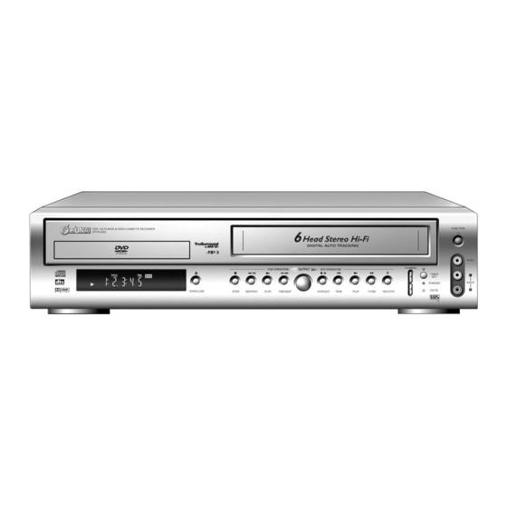
Page 1: Dvd Player
I Specifications I Alignment for Mechanism I Preparation for Servicing I Exploded views I Disassembly/Assembly of Mechanism I Parts List I Adjustment Procedures I Alignment Procedures of Mechanism I Schematic Diagrams I CBA’s DVD PLAYER & VIDEO CASSETTE RECORDER DPVR-2600/DPVR-2700 DPVR-2605... -
Page 2: Table Of Contents
MAIN SECTION DVD PLAYER & VIDEO CASSETTE RECORDER DPVR-2600/DPVR-2700/DPVR-2605 Sec. 1: Main Section I Specifications I Preparation for Servicing I Adjustment Procedures I Schematic Diagrams I CBA’s TABLE OF CONTENTS Specifications................1-1-1 Laser Beam Safety Precautions . -
Page 3: Specifications
SPECIFICATIONS < VCR Section > Description Unit Minimum Nominal Maximum Remark 1. Video 1-1. Video Output (PB) Vp-p SP Mode 1-2. Video Output (R/P) Vp-p SP Mode, 1-3. Video S/N Y (R/P) W/O Burst 1-4. Video Color S/N AM (R/P) SP Mode 1-5. -
Page 4: Dvd Section
< DVD Section > ITEM CONDITIONS UNIT NOMINAL LIMIT 1. Video Output 75 ohm load 2. Optical Digital Out 3. Audio (PCM) 3-1. Output Level 1kHz 0dB Vrms 3-2. S/N 3-3. Freq. Response fs=48kHz 20~22kHz ± 2 fs=44.1kHz 20~20 kHz ±... -
Page 5: Laser Beam Safety Precautions
LASER BEAM SAFETY PRECAUTIONS This DVD player uses a pickup that emits a laser beam. Do not look directly at the laser beam coming from the pickup or allow it to strike against your skin. The laser beam is emitted from the location shown in the figure. When checking the laser diode, be sure to keep your eyes at least 30cm away from the pickup lens when the diode is turned on. -
Page 6: Important Safety Precautions
IMPORTANT SAFETY PRECAUTIONS Product Safety Notice I. Also check areas surrounding repaired locations. J. Be careful that foreign objects (screws, solder Some electrical and mechanical parts have special droplets, etc.) do not remain inside the set. safety-related characteristics which are often not evi- K. -
Page 7: Safety Check After Servicing
Safety Check after Servicing Examine the area surrounding the repaired location for damage or deterioration. Observe that screws, parts, Chassis or Secondary Conductor and wires have been returned to their original posi- tions. Afterwards, do the following tests and confirm the specified values to verify compliance with safety Primary Circuit Terminals standards. -
Page 8: Standard Notes For Servicing
STANDARD NOTES FOR SERVICING Circuit Board Indications How to Remove / Install Flat Pack-IC a. The output pin of the 3 pin Regulator ICs is indi- 1. Removal cated as shown. With Hot-Air Flat Pack-IC Desoldering Machine:. (1) Prepare the hot-air flat pack-IC desoldering Top View Bottom View machine, then apply hot air to the Flat Pack-IC... - Page 9 With Soldering Iron: (4) Bottom of the flat pack-IC is fixed with glue to the CBA; when removing entire flat pack-IC, first apply (1) Using desoldering braid, remove the solder from all soldering iron to center of the flat pack-IC and heat pins of the flat pack-IC.
- Page 10 2. Installation Instructions for Handling Semi-conductors (1) Using desoldering braid, remove the solder from the foil of each pin of the flat pack-IC on the CBA Electrostatic breakdown of the semi-conductors may so you can install a replacement flat pack-IC more occur due to a potential difference caused by electro- easily.
-
Page 11: Preparation For Servicing
PREPARATION FOR SERVICING How to Enter the Service Mode About REC-Safety Switch Caution: The REC-Safety Switch is directly mounted on the About Optical Sensors Main CBA. When the Deck Mechanism Assembly is Caution: removed from the Main CBA for servicing, this switch does not work automatically. -
Page 12: Cabinet Disassembly Instructions
CABINET DISASSEMBLY INSTRUCTIONS 1. Disassembly Flowchart REMOVAL REMOVE/*UNHOOK/ This flowchart indicates the disassembly steps to gain LOC. PART Fig. UNLOCK/RELEASE/ Note access to item(s) to be serviced. When reassembling, UNPLUG/DESOLDER follow the steps in reverse order. Bend, route, and dress the cables as they were originally. DVD Main 3(S-5), *CN101, [1] Top Cover... - Page 13 Reference Notes [1] Top Cover CAUTION 1: Locking Tabs (L-1) and (L-2) are fragile. (S-1) Be careful not to break them. (S-1) 1-1. Connect the wall plug to an AC outlet and press the OPEN/CLOSE button to open the Tray. 1-2.
- Page 14 (S-4) CN701 (S-7) CN501 [7] Rear Panel (S-4) (S-6) (S-6) (S-7) [5] DVD Mecha Assembly Fig. D6 Fig. D4 (S-8) (S-9) (S-5) (S-5) CN101 [6] DVD Main (S-5) (S-8) CBA Unit (S-8) (S-9) CN401 [8] VCR Chassis DVD Mecha Unit Assembly CN002 Short the three short lands by soldering...
- Page 15 FE Head Cylinder Assembly AC Head Assembly SW507 LD-SW [9] Deck Assembly [10] Main CBA [12] AFV CBA CN2002 [9] Deck Assembly Cam Gear Hole Shaft Desolder Hole Desolder [11] Function CBA LD-SW from bottom [10] Main CBA (S-10) [10] Main CBA From Cylinder From...
- Page 16 Bracket (S-11) (S-12) (S-11) [13] Power Supply CBA (W-1) (S-13) [15] Deck Pedestal-2 (L-3) (W-1) [17] Insulator (W-1) [16] Side Bracket [14] Deck Pedestal-1 (S-14) Fig. D9 HOW TO MANUAL EJECT 1. Remove the Top Case. 2. Make a tool from a paper clip, etc., (length = approxi- mately 50 mm, maximum diameter = approximately 3 mm) as shown below.
-
Page 17: Electrical Adjustment Instructions
ELECTRICAL ADJUSTMENT INSTRUCTIONS Head Switching Position Adjustment General Note: "CBA" is an abbreviation for "Circuit Board Assembly." Purpose: NOTE: To determine the Head Switching point during 1.Electrical adjustments are required after replacing playback. circuit components and certain mechanical parts. Symptom of Misadjustment: It is important to do these adjustments only after all repairs and replacements have been com- May cause Head Switching noise or vertical jitter... -
Page 18: Firmware Renewal Mode
FIRMWARE RENEWAL MODE 1. Turn the power on and remove the disc on the tray. 2. To put the DVD player into version up mode, press [9], [8], [7], [6], and [SEARCH MODE] buttons on the remote control unit in that order. The tray will open automatically. -
Page 19: Block Diagrams
BLOCK DIAGRAMS <VCR Section> Servo/System Control Block Diagram NOTE FOR WIRE CONNECTORS: 1. PREFIX SYMBOL "CN" MEANS CONNECTOR. IC501 FRONT JACK CBA (CAN DISCONNECT AND RECONNECT.) (SERVO/SYSTEM CONTROL) MAIN CBA 2. PREFIX SYMBOL "CL" MEANS WIRE-SOLDER HOLES OF THE PCB. CN505 CN651 (WIRE IS SOLDERED DIRECTLY.) - Page 20 Video Block Diagram REC-VIDEO SIGNAL PB-VIDEO SIGNAL DVD VIDEO SIGNAL MODE: SP/REC MAIN CBA IIC-BUS SCL TO SERVO/SYSTEM IIC-BUS SDA CONTROL BLOCK JK101 DVD-R FROM DVD VIDEO BLOCK DVD-G IC501 (OSD) <DVD SECTION> DVD-B Q301 CHARACTER BUFFER TU701 VIDEO TU-VIDEO IC301 (Y/C SIGNAL PROCESS) (DECK ASSEMBLY)
- Page 21 Audio Block Diagram PB-AUDIO SIGNAL REC-AUDIO SIGNAL Mode : SP/REC MAIN CBA N-A-PB TO Hi-Fi N-A-REC AUDIO BLOCK IC301 (AUDIO SIGNAL PROCESS) TUNER PB-ON LINE MUTE (DECK ASSEMBLY) SP/LP-ON ACE HEAD ASSEMBLY REC-ON Q404 CL287 CL504 A-PB/REC 4 AUDIO 4 A-PB/REC Q403 HEAD A-COM 3...
- Page 22 Hi-Fi Audio Block Diagram DVD AUDIO SIGNAL PB-AUDIO SIGNAL REC-AUDIO SIGNAL Mode : SP/REC IC751 (SW) JK101 MAIN CBA A-IN1(R) A-IN1(L) Q101 A-OUT1(R) BUFFER A-OUT1(L) Q102 JK102 BUFFER SW CTL A-IN2(R) A-IN2(L) A-OUT2(R) A-OUT2(L) Q752 TO SYSTEM OUTPUT SELECT CONTROL BLOCK JK751 DVD-A(R)
- Page 23 Power Supply Block Diagram NOTE : CAUTION CAUTION ! FOR CONTINUED PROTECTION AGAINST FIRE HAZARD, Fixed voltage (or Auto voltage selectable ) power supply circuit is used in this unit. The voltage for parts in hot circuit is measured using If Main Fuse (F001) is blown, check to see that all components in the power supply REPLACE ONLY WITH THE SAME TYPE T1.6AL/250V FUSE.
- Page 24 BLOCK DIAGRAMS < DVD Section > DVD System Control Block Diagram NOTE FOR WIRE CONNECTORS: 1. PREFIX SYMBOL "CN" MEANS CONNECTOR. (CAN DISCONNECT AND RECONNECT.) 2. PREFIX SYMBOL "CL" MEANS WIRE-SOLDER HOLES OF THE PCB. (WIRE IS SOLDERED DIRECTLY.) IC601 (DVD HOST PROCESSOR) IC2001 IC301...
- Page 25 RF Signal Process/Servo Block Diagram DATA(VIDEO/AUDIO) SIGNAL FOCUS SERVO SIGNAL TRACKING SERVO SIGNAL SLIDE SERVO SIGNAL DISK SERVO SIGNAL IC101 (RF SIGNAL PROCESS) PICK-UP UNIT DVD MAIN CBA UNIT HOLD TESTSG CN101 FROM/TO DVD SIGNAL PROCESS BLOCK DIAGRAM NARF C 10 DETECTOR BDO DET INPUT...
- Page 26 DVD Signal Process Block Diagram DATA(VIDEO/AUDIO) SIGNAL DVD MAIN CBA UNIT IC201 (DVD SIGNAL PROCESS) PARA0 PARA1 PARA2 DATA VIDEO/AUDIO PARA3 TO DVD VIDEO SLICER PARA0-PARA7 DEMODULATOR FROM/TO RF SIGNAL INTERFACE BLOCK DIAGRAM NARF PARA4 PROCESS/SERVO PARA5 BLOCK DIAGRAM TESTSG PARA6 PARA7 MEMORY...
- Page 27 DVD Video Block Diagram DATA(VIDEO) SIGNAL DATA(AUDIO) SIGNAL VIDEO SIGNAL DATA(VIDEO/AUDIO) SIGNAL IC601 (DVD HOST PROCESSOR) CACHE SUBSYSTEM FROM DVD PARA0 INTERNAL CENTRAL FRONT-END PCM-BCK SIGNAL PROCESS PARA0-PARA7 PERIPHERALS COMMAND & LINK PCM-DATA0 BLOCK DIAGRAM PARA7 TO DVD PORTS PORT INTERFACE PCM-SCLK AUDIO...
- Page 28 DVD Audio Block Diagram DATA(AUDIO) SIGNAL AUDIO SIGNAL IC1204 FIBER OPTIC TRANS MODULE CN701 CN1601 Q1351 JK1202 SPDIF BUFFER DIGITAL AUDIO OUT IC801 (AUDIO DAC) IC1201 (AMP) SPDIF CN701 CN1601 DVD-A(L) 4X/8X L-CH PCM-BCK ENPHANCED LPF+AMP DVD-AUDIO-L TO AUDIO OVERSAMPLING PCM-DATA0 SERIAL MULTI-LEVEL...
-
Page 29: Schematic Diagrams / Cba's And Test Points
SCHEMATIC DIAGRAMS / CBA’S AND TEST POINTS Standard Notes Notes: WARNING 1. Do not use the part number shown on these draw- ings for ordering. The correct part number is shown Many electrical and mechanical parts in this chassis in the parts list, and may be slightly different or have special characteristics. - Page 30 LIST OF CAUTION, NOTES, AND SYMBOLS USED IN THE SCHEMATIC DIAGRAMS ON THE FOLLOWING PAGES: 1. CAUTION: FOR CONTINUED PROTECTION AGAINST FIRE HAZARD, REPLACE ONLY WITH THE SAME TYPE FUSE. 2. CAUTION: Fixed Voltage (or Auto voltage selectable) power supply circuit is used in this unit. If Main Fuse (F1001) is blown, first check to see that all components in the power supply circuit are not defec- tive before you connect the AC plug to the AC power supply.
- Page 31 Main 1/7 Schematic Diagram < VCR Section > Note: When it is necessary to replace one or more of the following Diodes, all three should be replaced: D506, D507, D508. 1-10-3 1-10-4 1-10-5 H9300SCM1...
- Page 32 Main 2/7 Schematic Diagram < VCR Section > 1-10-6 1-10-8 H9300SCM2 1-10-7...
- Page 33 Main 3/7 Schematic Diagram < VCR Section > 1-10-9 1-10-10 1-10-11 H9300SCM3...
- Page 34 Main 4/7 Schematic Diagram < VCR Section > 1-10-12 1-10-13 1-10-14 H9300SCM4...
- Page 35 Main 5/7 Schematic Diagram < VCR Section > H9300SCM5 1-10-15 1-10-16...
- Page 36 Main 6/7 Schematic Diagram < VCR Section > H9300SCM6 1-10-17 1-10-18...
- Page 37 Main 7/7 Schematic Diagram < VCR Section > 1-10-19 1-10-20 H9300SCM7...
-
Page 38: Power Supply Schematic Diagram
Power Supply Schematic Diagram < VCR Section > CAUTION ! NOTE : CAUTION Fixed voltage (or Auto voltage selectable ) power supply circuit is used in this unit. THE VOLTAGE FOR PARTS IN HOT CIRCUIT IS MEASURED USING FOR CONTINUED PROTECTION AGAINST FIRE HAZARD, If Main Fuse (F001) is blown, check to see that all components in the power supply HOT GND AS A COMMON TERMINAL. - Page 39 Function Schematic Diagram < VCR Section > FL2001 MATRIX CHART STANDBY REPEAT STANDBY TITLE CHP. TRK. REPEAT TITLE CHP. TRK. 1-10-23 1-10-24 H9300SCF...
- Page 40 AFV Schematic Diagram < VCR Section > Comparison Chart of Models and Marks MODEL MARK DPVR-2600 DPVR-2700 DPVR-2605 1-10-25 1-10-26 H9300SCAFV...
- Page 41 Front Jack Schematic Diagram < VCR Section > Note: When it is necessary to replace one or more of the following Diodes, all four should be replaced: D652, D653, D654, D655. H9300SCJ Front Jack CBA Top View Front Jack CBA Bottom View BH9311F01012-C 1-10-27 1-10-28...
- Page 42 Power Supply CBA Top View Power Supply CBA Bottom View CAUTION ! BECAUSE A HOT CHASSIS GROUND IS PRESENT IN THE POWER NOTE : CAUTION Fixed voltage ( or Auto voltage selectable ) power supply circuit is used in this unit. SUPPLY CIRCUIT , AN ISOLATION TRANSFORMER MUST BE USED.
- Page 43 Function CBA Top View Function CBA Bottom View BH9311F01012-B 1-10-31 1-10-32...
- Page 44 AFV CBA Top View AFV CBA Bottom View Junction-A CBA Top View Junction-A CBA Bottom View BH9311F01012-E Junction-B CBA Top View Junction-B CBA Bottom View BHC400F01091 BH9311F01012-F 1-10-33 1-10-34...
- Page 45 Main CBA Top View Sensor CBA Top View ( End Sensor ) BHB300F01011-A TP751 V-OUT BHB300F01011-B TP301 C-PB Sensor CBA Top View ( Start Sensor ) BHB300F01011-A BHB300F01011-B TP502 END-S VR501 SW-P TP503 TP504 RF-SW TP501 S-INH 1-10-35 1-10-36 1-10-37 BH9311F01012-A...
- Page 46 Main CBA Bottom View 1-10-38 1-10-39 1-10-40 BH9311F01012-A...
- Page 47 DVD Main 1/4 Schematic Diagram < DVD Section > 1-10-41 1-10-42 1-10-43 H9300SCD1...
- Page 48 DVD Main 2/4 Schematic Diagram < DVD Section > 1-10-44 1-10-45 1-10-46 H9300SCD2...
- Page 49 DVD Main 3/4 Schematic Diagram < DVD Section > 1-10-47 1-10-48 1-10-49 H9300SCD3...
- Page 50 DVD Main 4/4 Schematic Diagram < DVD Section > 1-10-50 1-10-51 1-10-52 H9300SCD4...
-
Page 51: Waveforms
WAVEFORMS (TP751 of Main CBA) V-OUT E-E 10usec 50mV x 10 (TP751 of Main CBA) UPPER (TP302 of Main CBA) LOWER V-OUT 0.1V x 10 RF-SW 0.5V x 10 50usec (TP301 of Main CBA) UPPER (TP302 of Main CBA) LOWER C-PB 10mV x 10 RF-SW... - Page 52 WAVEFORMS NOTE: Input CD: 1kHz PLAY (WF4~WF6) DVD: POWER ON (STOP) MODE (WF1~WF3) Pin 5 of CN1601 Pin 13 of CN1601 0.2V 20usec VIDEO-Y 0.5msec AUDIO-L Pin 7 of CN1601 Pin 15 of CN1601 VIDEO-CVBS 0.5V 20usec AUDIO-R 0.5msec Pin 9 of CN1601 Pin 18 of CN1601 VIDEO-C 0.2V...
- Page 53 WIRING DIAGRAM < VCR SECTION > REAR S-VIDEO DIGITAL AUDIO AUDIO AUDIO OUT OUT (R) OUT (L) ANT-IN ANT-OUT CN651 CN505 CN1001 1 GND VIDEO P-ON+1.8V KEY-2 P-ON+1.8V CN002 CN051 CL051 3 AL+5V EV+2.5V 1 AL+44V AL+44V CAS-LED EV+2.5V FRONT JACK CBA AC CORD AUDIO AL+12V...
- Page 54 WIRING DIAGRAM< DVD SECTION> DVD MECHA LOADING RELAY CBA MOTOR CN501 P-ON+1.8V 1 P-ON+1.8V 2 EV+2.5V 3 TRAY-OUT CN3001 CN401 EV+2.5V 4 1 LM(+) P-ON+5V 2 LM(-) P-ON+5V 6 SPINDLE SW CBA TRAY-IN 3 TRAY-IN MOTOR GND 7 4 TRAY-OUT GND 8 5 GND GND 9...
-
Page 55: Ic Pin Function Descriptions
IC PIN FUNCTION DESCRIPTIONS [ VCR Section ] Signal Active Function Name Level IC501( SERVO / SYSTEM CONTROL IC ) POWER “POWER” LED 23 OUT Signal Output “H” ≥ 4.5V, “L” ≤ 1.0V “CASSETTE” LED 24 OUT CAS LED Signal Active Signal Output Function... - Page 56 Signal Active Signal Active Function Function Name Level Name Level H/L/ 52 OUT OSD-V- OSD Video Signal 81 OUT LM-FWD/ Loading Motor Output Control Signal Hi-z DVD Power Control DVD- OSDVcc OSDVcc 82 OUT POWER Signal LPF Connected 83 OUT A-MUTE- Audio Mute Control Terminal (Slicer) Signal (Mute = “H”)
- Page 57 IC2001 [ PT6315-S(TP) ] Signal In/Out Name Function Name Clock Input Serial Interface Strobe Key Data 1 Input Key Data 2 Input Power Supply a / KEY-1 Segment Output / Key Souce-1 b / KEY-2 Segment Output / Key Souce-2 Segment Output d / KEY-4 Segment Output/ Key Souce-4...
-
Page 58: Lead Identifications
LEAD IDENTIFICATIONS FS2KM-18A 2SC1815-BL(TPE2) NJM4558D BN1F4M-T KIA78R33PI 2SC1815-Y(TPE2) KIA4558P BA1F4M-T PQ3RD13(1A) 2SC1815-GR(TPE2) KTA1266(GR) KIA78R33API 2SC2120-Y(TPE2) KTC3199(Y,GR,BL) KTC3203(Y) 2SC2785(J,H,F,K) KTC3205 (Y) KRC103M 2SA966(Y) KRA103M 2SC2001(K,L) BN1L3Z(P) 2SA1020(Y) KRA110M 2SB892(S) KTA1273(Y) 2SC3266-Y(TPE2) KTA1281(Y) 2SA1015-GR(TPE2) KRA104M BN1L4M-T KRC110M-AT E C B E C B G D S BA1L3Z-T QSZAA0RMB131... - Page 59 DECK MECHANISM SECTION DVD PLAYER & VIDEO CASSETTE RECORDER DPVR-2600/DPVR-2700/DPVR-2605 Sec. 2: Deck Mechanism Section I Standard Maintenance I Alignment for Mechanism I Disassembly/Assembly of Mechanism I Alignment Procedures of Mechanism TABLE OF CONTENTS Standard Maintenance..............2-1-1 Service Fixtures and Tools .
-
Page 60: Standard Maintenance
STANDARD MAINTENANCE Service Schedule of Components H: Hours : Check I: Change Deck Periodic Service Schedule Ref.No. Part Name 1,000 H 2,000 H 3,000 H 4,000 H Cylinder Assembly Loading Motor Assembly Pulley Assembly Tension Lever Sub Assembly AC Head Assembly B573,B574 Reel S, Reel T Capstan Motor... - Page 61 Cleaning Cleaning of Audio Control Head Clean the head with a cotton swab. Cleaning of Video Head Procedure Clean the head with a head cleaning stick or chamois 1.Remove the top cabinet. cloth. 2.Dip the cotton swab in 90% isopropyl alcohol and Procedure clean the audio control head.
-
Page 62: Service Fixtures And Tools
SERVICE FIXTURE AND TOOLS J-1-1, J-1-2 Ref. No. Name Part No. Adjustment J-1-1 Alignment Tape FL6A Head Adjustment of Audio Control Head J-1-2 Alignment Tape FL6N8 Azimuth and X Value Adjustment of Audio Control (1 speed only) Head / Adjustment of Envelope Waveform FL6NS8 (2 speed only) Guide Roller Adj.Screwdriver... -
Page 63: Mechanical Alignment Procedures
MECHANICAL ALIGNMENT PROCEDURES Explanation of alignment for the tape to correctly run B. Method to place the Cassette Holder in the tape- starts on the next page. Refer to the information below loaded position without a cassette tape on this page if a tape gets stuck, for example, in the 1. -
Page 64: Tape Interchangeability Alignment
1.Tape Interchangeability Alignment Note: To do these alignment procedures, make sure that the Tracking Control Circuit is set to the center position every time a tape is loaded or unloaded. (Refer to page 2-3-4, procedure 1-C, step 2.) Equipment required: Dual Trace Oscilloscope VHS Alignment Tape (FL6NS8) Guide Roller Adj. - Page 65 1-A. Preliminary/Final Checking and 3. Check to see that the tape runs without creasing at Alignment of Tape Path Take-up Guide Post [4] or without snaking between Guide Roller [3] and AC Head. (Fig. M3 and M5) Purpose: 4. If creasing or snaking is apparent, adjust the Tilt To make sure that the tape path is well stabilized.
- Page 66 6. Press CH DOWN button on the unit until the CTL 1-D. Azimuth Alignment of Audio/Control/ waveform has shifted from its original position (not Erase Head the position achieved in step 5, but the position of Purpose: CTL waveform in step 4) by approximately -2msec. To correct the Azimuth alignment so that the Audio/ Make sure that the envelope is simply attenuated Control/Erase Head meets tape tracks properly.
-
Page 67: Disassembly/Assembly Procedures Of Deck Mechanism
DISASSEMBLY/ASSEMBLY PROCEDURES OF DECK MECHANISM Before following the procedures described below, be sure to remove the deck assembly from the cabinet. (Refer to CABINET DISASSEMBLY INSTRUCTIONS on page 1-6-1.) All the following procedures, including those for adjustment and replacement of parts, should be done in Eject mode;... - Page 68 REMOVAL INSTALLATION STEP START- REMOVE/*UNHOOK/ /LOC. PART ADJUSTMENT Fig. No. UNLOCK/RELEASE/ CONDITION UNPLUG/DESOLDER Loading Arm S(B) (+)Refer to Alignment [35] [25] DM2,DM15 Assembly Sec.Pg.2-4-9 Loading Arm T(B) (+)Refer to Alignment [36] [35] DM2,DM15 Assembly Sec.Pg.2-4-9 [2],[25] M Brake T(HI) Assembly DM1,DM16 *(P-6) [37] [38]...
-
Page 69: Top View
Top View [45] [46] [50] [47] [14] [13] [11] [15] [39] [40] [10] [12] [38] [37] [44] [33] [42] [31] [32] [41] [43] Fig. DM1 Bottom View [19] [36] [35] [24] [26] [27] [25] [23] [28] [22] [29] [20] [34] Fig. - Page 70 (S-1) (S-1) (S-2) (P-1) (S-4) (S-3) Fig. DM5 Fig. DM3 [50] Type A Pin D Pin C Type B [51] [50] (L-9) Pull up Slide Pin A (L-8) Pin B Slot A Slots B (S-5) Slot A First, while pushing the locking tab as shown in the right, slide and pull up the right side on [2] to release Pin A and Pin B from the slots A.
- Page 71 (S-7) (S-9) [14] (S-10) [15] Desolder from bottom (S-6) Lead with White Stripe Belt View for A Fig. DM7 Fig. DM9 (L-2) Adj. Screw [17] After removing the Screw (S-11), [11] while pressing the Locking Tab (L-3) (L-1) (L-3), remove [16]. (P-3) [16] [13]...
- Page 72 (C-1) Cap Belt [20] [19] [21] Fig. DM12 (S-12) Fig. DM11 2-4-6 DUALPALDA...
- Page 73 [25] (C-5) (C-2) (C-3) [22] [23] (S-15) [26] (L-4) (P-4) [27] (C-6) [29] (C-4) [28] [30] [24] [31] (P-4) [28] [32] When installing [23], install the spring (P-4) to [28] as Position of Mode Lever when installed shown in the left figure, and Pin of [38] then install [23] while Pin on...
- Page 74 Refer to the Alignment Section, Page 2-4-9. [46] [45] [47] (P-5) (L-7) [34] [33] [36] [35] (L-5) Fig. DM17 Fig. DM15 [39] (C-8) [42] (C-7) (P-7) [44] [41] turn (L-6) [43] [48] [49] Slide (P-6) [38] turn [37] [40] Fig. DM18 turn Fig.
-
Page 75: Alignment Procedures Of Mechanism
ALIGNMENT PROCEDURES OF MECHANISM Alignment 1 The following procedures describe how to align the individual gears and levers that make up the tape Loading Arm, S and T Assembly loading/unloading mechanism. Since information about the state of the mechanism is provided to the Install Loading Arm S and T Assembly so that their System Control Circuit only through the Mode Switch, triangle marks point to each other as shown in Fig. - Page 76 Alignment 3 Cam Gear (A), Rack Assembly Install the Rack Assembly so that the first tooth on the gear of the Rack Assembly meets the first groove on the Cam Gear (A) as shown in Fig. AL4. Cam Gear (A) Top View Alignment 3 First tooth...
- Page 77 EXPLODED VIEWS AND PARTS LIST SECTION DVD PLAYER & VIDEO CASSETTE RECORDER DPVR-2600/DPVR-2700/DPVR-2605 Sec. 3: Exploded views and Parts List Section I Exploded views I Parts List TABLE OF CONTENTS Exploded Views ............... . 3-1-1 Mechanical Parts List.
-
Page 78: Exploded Views
2B15 AC1001 Sensor CBA 2L051 Sensor CBA 2B40 2L036 2L022 2L022 2L035 2B39 2B39 2L031 2L022 2B16 2L051 2L022 2L062 2L022 2L031 2B39 2L032 2L031 2L052 2L052 2L037 2B13 2B20 [ DPVR-2600/DPVR-2700 ] Front Jack CBA JW002 3-1-1 3-1-2 H9300CEX... - Page 79 Packing [ B ] Some Ref. Numbers are not in sequence. Unit 3-1-3 H9300PEX...
- Page 80 DECK EXPLODED VIEWS Deck Mechanism View 1 Mark Description (Blue grease) Floil G-374G SLIDUS OIL #150 L1467 B494 B553 L1191 B411 B567 L1053 B410 L1051 Chassis Assembly Top View (Lubricating Point) B501 B560 L1450 B426 L1466 B121 B126 L1468 B492 B571 Some Ref.
- Page 81 Deck Mechanism View 2 Mark Description B587 Note: Both TENSION Floil G-374G (Blue grease) LEVER ASSEMBLY MK11(B27) and the TENSION SANKOUL FG84M (Yellow grease) LEVER ASSEMBLY MK11 (B587) can be used. B574 B508 B148 B487 B573 L1406 B522 B518 B520 B521 B564 B499...
- Page 82 Deck Mechanism View 3 Mark Description Floil G-374G (Blue grease) L1321 B347 Note: There are two different, but interchangeable types of CLEANER LEVER(B359) in this model, and have different combination with B361. Please L1321 see Table 1 for details and combination. (Refer to DECK PARTS LIST section.) Table 1 (B359 and B361 Combination) B359 CLEANER LEVER...
-
Page 83: Mechanical Parts List
0DM400731C Comparison Chart of Models and Marks ACCESSORIES Model Mark REMOTE CONTROL UNIT 364/CRC006 NA204ED DRY BATTERY R6P/2S or XB0M451T0001 DPVR-2600 DRY BATTERY(SUNRISE) R6SSE/2S or XB0M451MS002 DPVR-2700 DRY BATTERY ES-GR6M-C XB0M571GLP01 DPVR-2605 RF CORD PAL 1.2M WPZ0122LG001 ACCESSORY BAG K8092BA... -
Page 84: Electrical Parts List
ELECTROLYTIC CAP. 470µF/6.3V M CE0KMASTL471 C108 ELECTROLYTIC CAP. 470µF/6.3V M or CE0KMASDL471 Model Mark ELECTROLYTIC CAP. 470µF/6.3V M CE0KMASTL471 DPVR-2600 C109 CHIP CERAMIC CAP. CH J 470pF/50V or CHD1JJ3CH471 DPVR-2700 CHIP CERAMIC CAP. CG J 470pF/50V CHD1JJ3CG471 DPVR-2605 C110 CHIP CERAMIC CAP. B K 2200pF/50V... - Page 85 Ref. No. Mark Description Part No. Ref. No. Mark Description Part No. C308 CHIP CERAMIC CAP. F Z 0.1µF/50V or CHD1JZ30F104 CHIP CERAMIC CAP. CG J 15pF/50V CHD1JJ3CG150 CHIP CERAMIC CAP. F Z 0.1µF/25V or CHD1EZ30F104 C343 ELECTROLYTIC CAP. 10µF/16V M H7 CE1CMAVSL100 CHIP CERAMIC CAP.
- Page 86 Ref. No. Mark Description Part No. Ref. No. Mark Description Part No. C464 CHIP CERAMIC CAP. F Z 0.1µF/50V or CHD1JZ30F104 C538 CHIP CERAMIC CAP. CH J 180pF/50V or CHD1JJ3CH181 CHIP CERAMIC CAP. F Z 0.1µF/25V or CHD1EZ30F104 CHIP CERAMIC CAP. CG J 180pF/50V CHD1JJ3CG181 CHIP CERAMIC CAP.
- Page 87 Ref. No. Mark Description Part No. Ref. No. Mark Description Part No. C1067 CHIP CERAMIC CAP. B K 0.01µF/50V CHD1JK30B103 C1481 ELECTROLYTIC CAP. 1µF/50V M or CE1JMASDL1R0 C1068 CHIP CERAMIC CAP. B K 0.01µF/50V CHD1JK30B103 ELECTROLYTIC CAP. 1µF/50V M CE1JMASTL1R0 C1201 ELECTROLYTIC CAP.
- Page 88 Ref. No. Mark Description Part No. Ref. No. Mark Description Part No. D118 ZENER DIODE DZ-11BSAT265 or NDTA00DZ11BS FIBER OPTIC TRANS.MODULE JWHHA00SH003 GP1FA512TZV ZENER DIODE MTZJT-7711A QDTA00MTZJ11 IC1402 DRIVER FOR DVD(6CH) MM1567AJ QSZBA0SMM084 D119 ZENER DIODE DZ-11BSAT265 or NDTA00DZ11BS COILS ZENER DIODE MTZJT-7711A QDTA00MTZJ11 L051...
- Page 89 Ref. No. Mark Description Part No. Ref. No. Mark Description Part No. TRANSISTOR KTC3199(GR) or NQS10KTC3199 TRANSISTOR 2SC1815-GR(TPE2) QQS102SC1815 TRANSISTOR 2SC2785(J) or QQSJ02SC2785 Q502 TRANSISTOR KTC3199(Y) or NQSY0KTC3199 TRANSISTOR 2SC2785(H) or QQSH02SC2785 TRANSISTOR KTC3199(GR) or NQS10KTC3199 TRANSISTOR 2SC2785(F) or QQSF02SC2785 TRANSISTOR 2SC2785(J) or QQSJ02SC2785 TRANSISTOR 2SC1815-Y(TPE2) or...
- Page 90 Ref. No. Mark Description Part No. Ref. No. Mark Description Part No. CARBON RES. 1/4W J 1k Ω RES. BUILT-IN TRANSISTOR BA1L3Z-T QQSZ00BA1L3Z R114 RCX4JATZ0102 CARBON RES. 1/4W J 1k Ω Q1054 TRANSISTOR KTC3205(Y) or NQSY0KTC3205 R116 RCX4JATZ0102 CARBON RES. 1/4W J 680 Ω TRANSISTOR 2SC3266-Y(TPE2) QQSY02SC3266 R117...
- Page 91 Ref. No. Mark Description Part No. Ref. No. Mark Description Part No. CHIP RES.(1608) 1/10W 0 Ω CARBON RES. 1/4W G 3.6k Ω R339 RRXAZR5Z0000 RCX4GATZ0362 CARBON RES. 1/6W J 820 Ω or CHIP RES.(1608) 1/10W J 68k Ω R401 RCX6JATZ0821 R512 RRXAJR5Z0683...
- Page 92 Ref. No. Mark Description Part No. Ref. No. Mark Description Part No. CHIP RES.(1608) 1/10W J 1k Ω CHIP RES.(1608) 1/10W J 1k Ω R583 RRXAJR5Z0102 R1225 RRXAJR5Z0102 CHIP RES.(1608) 1/10W J 100 Ω CHIP RES.(1608) 1/10W J 1k Ω R584 RRXAJR5Z0101 R1226...
- Page 93 Ref. No. Mark Description Part No. Ref. No. Description Part No. SW508 TACT SWITCH KSM0614B or SST0101HH013 CHIP CERAMIC CAP. FZ Z 0.1µF/50V CHD1JZ3FZ104 TACT SWITCH SKQSAF001A SST0101AL041 C2055 ELECTROLYTIC CAP. 22µF/50V M H7 CE1JMAVSL220 SW511 TACT SWITCH KSM0611B SST0101HH004 CONNECTOR SW2011 TACT SWITCH KSM0614B or...
- Page 94 Ref. No. Description Part No. Ref. No. Description Part No. D653 LED(GREEN) 204-10GD/S957 NPQZ10GDS957 PHOTO TRANSISTOR MID-32A22 NPWZM1D32A22 D654 LED(RED) 204HD/E NPQZ00204HDE LED EXCLUSIVE(B) POWER SUPPLY CBA D651 LED(RED) LTL-4211N NPQZLTL4211N D652 LED(RED) LTL-4211N NPQZLTL4211N Ref. No. Description Part No. D653 LED(GREEN) LTL-4231N NPQZLTL4231N...
- Page 95 Ref. No. Description Part No. Ref. No. Description Part No. FAST RECOVERY DIODE ERA18-04 QDPZ0ERA1804 CHOKE COIL 47µH-K LLBD00PKV005 D015 RECTIFIER DIODE FR202 NDQZ000FR202 L1007 CHOKE COIL 47µH-K or LLBD00PKV007 D019 PCB JUMPER D0.6-P10.0 JW10.0T CHOKE COIL 47µH-K LLBD00PKV005 D020 PCB JUMPER D0.6-P5.0 JW5.0T L1008...
- Page 96 Ref. No. Description Part No. Ref. No. Description Part No. CARBON RES. 1/6W J 100k Ω or R1038 RCX6JATZ0104 CHIP CERAMIC CAP. F Z 0.1µF/25V or CHD1EZ30F104 CARBON RES. 1/4W J 100k Ω RCX4JATZ0104 CHIP CERAMIC CAP. FZ Z 0.1µF/50V CHD1JZ3FZ104 CARBON RES.
-
Page 97: Deck Parts List
DECK PARTS LIST Notes: Ref. No. Description Part No. 1. There are two different, but interchangeable types of FE HEAD ASSEMBLY MK11 or N9742FEL CLEANER LEVER(B359) in this model, and have FE HEAD(MK11) MH-131SF11 or DHVEC01Z0005 different combination with B361. Please see Table 1 FE HEAD ASSEMBLY MK11 or N9743FEL for details and combination. - Page 98 Ref. No. Description Part No. B560 KICK SPRING MK10 0VM411475A B562 C DRIVE LEVER L MK10 0VM304408 B563 SLIDER SHAFT MK10 0VM411112 B564 M GEAR(HYT) N12G5F* 0VM412378 B565 SENSOR GEAR MK11 0VM305080 B567 PINCH ARM(B) MK10 0VM304396 B568 BT ARM MK10 0VM304417H B569 CAM HOLDER F MK11...
Need help?
Do you have a question about the DPVR-2600 and is the answer not in the manual?
Questions and answers