Advertisement
Quick Links
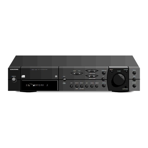
RCD 405
Service
Zusätzlich erforder-
Manual
liche Unterlagen
für den
RCD 405
Komplettservice:
Additionally
required Service
Sach-Nr./Part No.
Manuals for the
72010-752.30
Complete Service:
R C D 4 0 5
POWER IO
POWER IO
A N T E N N A
5 9
T U N E D
8 A E P A
RCD 405
RC 400
Das Gerät RCD 405 ist eine Weiterentwicklung des Gerätes RCD 400.
In diesem Service Manual sind nur die geänderten Platinenabbildungen,
Schaltpläne und die Ersatzteilliste enthalten.
Für den Service benötigen Sie die Service Manuals RCD 400, RCD
405 und das Service Manual "Sicherheit".
Änderungen vorbehalten
Subject to alteration
GRUNDIG Service
Service
Manual
Sicherheit
Safety
Sach-Nr./Part No.
72010-800.00
H I F I C D R E C E I V E R
STOP
STOP
R D S
OPEN/
OPEN/
INFO
INFO
CLOSE
CLOSE
3
SERVICE MANUAL
Service
Manual
RCD 400
Sach-Nr./Part No.
72010-747.05
TUNER BAND
TUNER BAND
PAUSE
PLAY
PAUSE
PLAY
SKIP/STATION
SKIP/STATION
CD
CD
SEARCH/TUNING
SEARCH/TUNING
SHUFFLE
REPEAT
EDIT
CANCEL
MEMORY
TAPE/AUX
SHUFFLE
REPEAT
EDIT
CANCEL
MEMORY
TAPE/AUX
MONO
ANT/CABLE
MONO
ANT/CABLE
(9.79810-8151 / G.LG 19-51)
(75954-032.17)
The unit RCD 405 is a modification of the unit RCD 400. In this Service
Manual only the altered PCBs, circuit diagrams and the spare parts list
are included.
For the Service the Service Manuals RCD 400, RCD 405 and the
Service Manual "Safety" are needed.
Printed in Germany
VK 232 1296
Allgemeiner Teil / General Section
DEFEAT
LOUDNESS
DEFEAT
LOUDNESS
TREBLE
TREBLE
VOLUME
VOLUME
-
+
-
+
BASS
BASS
-
+
+
-
BALANCE
BALANCE
L
R
L
R
HEADPHONES
HEADPHONES
Service Manual Sach-Nr.
Service Manual Part No.
*
RCD 405
S L E EP
P T Y
T U NE R
ST AT I ON
C D
–
DI S C
+
T AP E
-
+
V OL U M E
RC 400
72010-752.30
1 - 1
Advertisement

Subscribe to Our Youtube Channel
Related Manuals for Grundig RCD 405


Summary of Contents for Grundig RCD 405
- Page 1 (75954-032.17) Das Gerät RCD 405 ist eine Weiterentwicklung des Gerätes RCD 400. The unit RCD 405 is a modification of the unit RCD 400. In this Service In diesem Service Manual sind nur die geänderten Platinenabbildungen, Manual only the altered PCBs, circuit diagrams and the spare parts list are included.
-
Page 2: Allgemeiner Teil
Verdrahtungsplan ................ 3 - 14 Spare Parts List and Exploded Views Ersatzteilliste und Explosionszeichnungen Exploded View RCD 405 .............. 4 - 1 Explosionszeichnung RCD 405 ............ 4 - 1 Exploded View CD Drive Mechanism ........... 4 - 2 Explosionszeichnung CD-Laufwerk ..........4 - 2 Spare Parts List ................ -
Page 3: Technische Daten
RCD 405 Allgemeiner Teil / General Section Technische Daten Specifications Verstärker Amplifier Ausgangsleistung (DIN45500) Output power (DIN45500) Musikleistung (4Ω) ............2 x 80W Music (4Ω) ................ 2 x 80W Sinusleistung (4Ω, 0,7% Klirrfaktor, 1kHz) ....... 2 x 50W Nominal (4Ω, 0.7% distortion, 1kHz) ........ 2 x 50W... - Page 4 Platinenabbildungen und Schaltplänen / Layout of PCBs and Circuit Diagrams RCD 405 Platinenabbildungen und Schaltpläne / Layout of PCBs and Circuit Diagrams Platinenabbildungen – CD-Teil / Layout of the PCBs – CD Part Ansicht von der Lötseite / View of solder side...
- Page 5 RCD 405 Platinenabbildungen und Schaltpläne / Layout of PCBs and Circuit Diagrams RCD 405 Platinenabbildungen und Schaltpläne / Layout of PCBs and Circuit Diagrams Schaltbild – CD-Teil / Circuit Diagram – CD Part R101 ca. 1.5V +4.7V DOBM IC03 FLAGS...
- Page 6 Platinenabbildungen und Schaltpläne / Layout of PCBs and Circuit Diagrams RCD 405 Platinenabbildungen und Schaltpläne / Layout of PCBs and Circuit Diagrams RCD 405 Schaltbild – Tuner-Teil / Circuit Diagram – Tuner Part 100R IFOUT +12V 0...5P BF998 2.5V 3.1V...
- Page 7 RCD 405 Platinenabbildungen und Schaltplänen / Layout of PCBs and Circuit Diagrams GL7812 +12V +12V R104 2.5V 2.5V 2.5V 2.5V 3.3V FM - IF Q.D. POST BUFFER BUFFER 1U/100V +12V +19V C104 1.5V R118A AM-ZF 3.4V BC548B 1.8K LA1266 2.7V...
- Page 8 Platinenabbildungen und Schaltplänen / Layout of PCBs and Circuit Diagrams RCD 405 Platinenabbildung – Tuner-Teil / Layout of PCB – Tuner Part Ansicht von der Bestückungsseite / View of components BR0 BR1 BR2 C113 BR111 BR110 C112 C114 R119 R123...
- Page 9 RCD 405 Platinenabbildungen und Schaltpläne / Layout of PCBs and Circuit Diagrams RCD 405 Platinenabbildungen und Schaltpläne / Layout of PCBs and Circuit Diagrams Platinenabbildungen / Layout of PCBs: -Netzteilplatte / Mains Board -Kopfhörerplatte / Headphone Board -Hauptplatte / Main Board...
- Page 10 Platinenabbildungen und Schaltpläne / Layout of PCBs and Circuit Diagrams RCD 405 Platinenabbildungen und Schaltpläne / Layout of PCBs and Circuit Diagrams RCD 405 Platinenabbildungen / Layout of PCBs: -Klangreglerplatte / Tone Control Board Schaltbild / Circuit Diagram: -Hauptplatte / Main Board -Klangreglerplatte / Tone Control Board -Lautstärkeplatte / Volume Board...
- Page 11 RCD 405 Platinenabbildungen und Schaltpläne / Layout of PCBs and Circuit Diagrams RCD 405 Platinenabbildungen und Schaltpläne / Layout of PCBs and Circuit Diagrams -Regulatorplatte / Regulator Board -Display- und Tastenplatte / Display and Key Board TONE CONTROL BD. +12V...
- Page 12 Platinenabbildungen und Schaltpläne / Layout of PCBs and Circuit Diagrams RCD 405 Platinenabbildungen und Schaltpläne / Layout of PCBs and Circuit Diagrams RCD 405 Verdrahtungsplan / Wiring Diagram SPEAKERS TAPE LEFT RIGHT AM ANT. FM ANT. BU303 Netzteilplatte BU302 Mains Board...
- Page 13 RCD 405 Platinenabbildungen und Schaltplänen / Layout of PCBs and Circuit Diagrams Explosionszeichnungen und Ersatzteilliste / Exploded Views and Spare Parts List Explosionszeichnung – RCD 405 / Exploded View – RCD 405 GRUNDIG Service 4 - 1...
-
Page 15: Ersatzteilliste Spare Parts List
MSW NB 0207 4,7 OHM 5% LI BU 304 75954-010.37 KOPFHOERERBUCHSE/ R 204 75987-542.14 MSW NB 0207 4,7 OHM 5% LI 11 / 96 RCD 405 EAR PHONE SOCKET R 359 8705-260-074 MOW 0617 270 OHM 10% R 360 8705-260-074 MOW 0617 270 OHM 10% C 206 75954-012.18... - Page 16 POS. SACHNUMMER BEZEICHNUNG POS. SACHNUMMER BEZEICHNUNG POS. PART NUMBER DESCRIPTION POS. PART NUMBER DESCRIPTION IC 2 8305-260-340 IC LA 3401 SANYO IC 3 8305-260-166 IC LA 1266 SANYO IC 4 75954-015.47 IC SAA 6579T IC 5 75954-015.02 IC NJM 7812 A 19202-702.12 MW-VORKR.
Need help?
Do you have a question about the RCD 405 and is the answer not in the manual?
Questions and answers