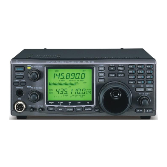
Icom IC-910H Service Manual
Service+manual+ic-910h
Hide thumbs
Also See for IC-910H:
- Service manual (104 pages) ,
- Instruction manual (88 pages) ,
- Programming manual (25 pages)
Table of Contents
Advertisement
Quick Links
Advertisement
Table of Contents

Related Manuals for Icom IC-910H


Summary of Contents for Icom IC-910H
- Page 1 Nov. 2008 SERVICE MANUAL ADDENDUM CONTENTS PARTS LIST ....... . 1 BOARD LAYOUTS .
- Page 2 Nov. 2008 SECTION 5. PARTS LIST [DISPLAY UNIT] [DISPLAY UNIT] ORDER ORDER DESCRIPTION DESCRIPTION 1140009671 S.IC M30622MAA-868FP (2355A-2) [EUR] 1750000550 S.DIO 1SS355 TE-17 [USA-1] 1140009671 S.IC M30622MAA-868FP (2355A-2) [USA] 1750000550 S.DIO 1SS355 TE-17 [KOR] 1140009671 S.IC M30622MAA-868FP (2355A-2) [AUS] 1750000550 S.DIO 1SS355 TE-17 [CHN] 1140009671 S.IC...
-
Page 3: Display Unit
Nov. 2008 [DISPLAY UNIT] [DISPLAY UNIT] ORDER ORDER DESCRIPTION DESCRIPTION 7030003520 S.RES ERJ3GEYJ 472 V (4.7K) R135 7030003360 S.RES ERJ3GEYJ 221 V (220) 7030003520 S.RES ERJ3GEYJ 472 V (4.7K) R136 7030003360 S.RES ERJ3GEYJ 221 V (220) 7030003680 S.RES ERJ3GEYJ 104 V (100K) R137 7030003360 S.RES ERJ3GEYJ 221 V (220) 7030003560 S.RES ERJ3GEYJ 103 V (10K) - Page 4 Nov. 2008 [DISPLAY UNIT] [DISPLAY UNIT] ORDER ORDER DESCRIPTION DESCRIPTION 4030006860 S.CER C1608 JB 1H 102K-T DS18 5040002950 S.LED TLGE1002A(T02) 4030006860 S.CER C1608 JB 1H 102K-T DS19 5040002950 S.LED TLGE1002A(T02) 4030006860 S.CER C1608 JB 1H 102K-T DS20 5040002950 S.LED TLGE1002A(T02) 4030006860 S.CER C1608 JB 1H 102K-T DS21 5040002950 S.LED...
- Page 5 Nov. 2008 [PLL UNIT] [PLL UNIT] ORDER ORDER DESCRIPTION DESCRIPTION 1130007700 S.IC BU4094BCF-E2 Q541 1530002601 S.TRA 2SC4215-O(TE85R,F) [KOR] IC12 1110001901 S.IC UPC4570G2-E1-A 1530002601 S.TRA 2SC4215-O(TE85R,F) [ITR] IC101 1130004831 S.IC TC7SU04F(TE85R,F) [EUR] 1530002601 S.TRA 2SC4215-O(TE85R,F) [CHN] 1130004830 S.IC TC7SU04F (TE85R) [USA] 1130004831 S.IC TC7SU04F(TE85R,F) [AUS]...
- Page 6 Nov. 2008 [PLL UNIT] [PLL UNIT] ORDER ORDER DESCRIPTION DESCRIPTION R107 7030007210 S.RES ERA3YEB 102V (1K) R326 7030003440 S.RES ERJ3GEYJ 102 V (1K) R108 7030007210 S.RES ERA3YEB 102V (1K) R327 7030003800 S.RES ERJ3GEYJ 105 V (1M) R109 7030007210 S.RES ERA3YEB 102V (1K) R330 7030003440 S.RES ERJ3GEYJ 102 V (1K) R110...
- Page 7 Nov. 2008 [PLL UNIT] [PLL UNIT] ORDER ORDER DESCRIPTION DESCRIPTION R625 7030003370 S.RES ERJ3GEYJ 271 V (270) C170 4030006860 S.CER C1608 JB 1H 102K-T R626 7030003230 S.RES ERJ3GEYJ 180 V (18) C171 4030008920 S.CER C1608 JB 1H 473K-T R627 7030003370 S.RES ERJ3GEYJ 271 V (270) C172 4030006860 S.CER C1608 JB 1H 102K-T R628...
- Page 8 Nov. 2008 [PLL UNIT] [MAIN UNIT] ORDER ORDER DESCRIPTION DESCRIPTION C404 4030006950 S.CER C1608 CH 1H 040C-T IC101 1110003141 IC LA1150N-E C405 4030009500 S.CER C1608 CH 1H 0R5B-T IC201 1110004840 S.IC NJM1496V-TE1-#ZZZB C407 4030006860 S.CER C1608 JB 1H 102K-T IC351 1110004870 S.IC TA4101F (TE12L.F) C408...
- Page 9 Nov. 2008 [MAIN UNIT] [MAIN UNIT] ORDER ORDER DESCRIPTION DESCRIPTION Q254 1530002691 S.TRA 2SC4116-GR(TE85R,F) [SWE] Q816 1530002691 S.TRA 2SC4116-GR(TE85R,F) [ITR] 1530002691 S.TRA 2SC4116-GR(TE85R,F) [USA-1] 1530002691 S.TRA 2SC4116-GR(TE85R,F) [CHN] 1530002691 S.TRA 2SC4116-GR(TE85R,F) [KOR] Q817 1530002691 S.TRA 2SC4116-GR(TE85R,F) [EUR] 1530002691 S.TRA 2SC4116-GR(TE85R,F) [ITR] 1530002690 S.TRA 2SC4116-GR (TE85R)
- Page 10 Nov. 2008 [MAIN UNIT] [MAIN UNIT] ORDER ORDER DESCRIPTION DESCRIPTION D305 1790000660 S.DIO MA728(TX) L1561 6200002041 S.COI NLV25T-101J D352 1790000620 S.DIO MA77(TX) L1562 6200002041 S.COI NLV25T-101J D401 1750000520 S.DIO DAN222TL L1563 6200002041 S.COI NLV25T-101J D402 1750000520 S.DIO DAN222TL L1564 6200002041 S.COI NLV25T-101J D491 1750000550 S.DIO...
- Page 11 Nov. 2008 [MAIN UNIT] [MAIN UNIT] ORDER ORDER DESCRIPTION DESCRIPTION R168 7030003540 S.RES ERJ3GEYJ 682 V (6.8K) R358 7510001581 S.THE NTCG16 4BH 153JT [USA] R169 7030003520 S.RES ERJ3GEYJ 472 V (4.7K) 7510001581 S.THE NTCG16 4BH 153JT [AUS] R201 7030003860 S.RES ERJ3GE JPW V 7510001580 S.THE NTCG16 4BH 153KT [SWE]...
- Page 12 Nov. 2008 [MAIN UNIT] [MAIN UNIT] ORDER ORDER DESCRIPTION DESCRIPTION R663 7030003330 S.RES ERJ3GEYJ 121 V (120) R951 7030003470 S.RES ERJ3GEYJ 182 V (1.8K) R664 7030003560 S.RES ERJ3GEYJ 103 V (10K) R952 7030003740 S.RES ERJ3GEYJ 334 V (330K) R665 7030003560 S.RES ERJ3GEYJ 103 V (10K) R953 7030003700 S.RES ERJ3GEYJ 154 V (150K) R666...
- Page 13 Nov. 2008 [MAIN UNIT] [MAIN UNIT] ORDER ORDER DESCRIPTION DESCRIPTION R1595 7030003680 S.RES ERJ3GEYJ 104 V (100K) R1718 7030003540 S.RES ERJ3GEYJ 682 V (6.8K) R1596 7030003680 S.RES ERJ3GEYJ 104 V (100K) R1719 7030003560 S.RES ERJ3GEYJ 103 V (10K) R1597 7030003680 S.RES ERJ3GEYJ 104 V (100K) R1720 7030003600 S.RES ERJ3GEYJ 223 V (22K) R1598...
- Page 14 Nov. 2008 [MAIN UNIT] [MAIN UNIT] ORDER ORDER DESCRIPTION DESCRIPTION R1872 7030003680 S.RES ERJ3GEYJ 104 V (100K) C255 4030010760 S.CER C1608 CH 1H 331J-T R1874 7030003680 S.RES ERJ3GEYJ 104 V (100K) C257 4030011600 S.CER C1608 JB 1E 104K-T R1875 7030003640 S.RES ERJ3GEYJ 473 V (47K) C258 4030007160 S.CER C1608 CH 1H 181J-T R1876...
- Page 15 Nov. 2008 [MAIN UNIT] [MAIN UNIT] ORDER ORDER DESCRIPTION DESCRIPTION C659 4030006900 S.CER C1608 JB 1H 103K-T C973 4030011600 S.CER C1608 JB 1E 104K-T C660 4030006900 S.CER C1608 JB 1H 103K-T C1007 4030011810 S.CER C1608 JB 1A 224K-T C661 4030006900 S.CER C1608 JB 1H 103K-T C1008 4510008550 S.ELE EEE1HA010SR...
- Page 16 Nov. 2008 [MAIN UNIT] [MAIN UNIT] ORDER ORDER DESCRIPTION DESCRIPTION C1675 4030006900 S.CER C1608 JB 1H 103K-T CP854 6910009670 S.CHE HK3-S-T C1676 4030006900 S.CER C1608 JB 1H 103K-T C1677 4510008550 S.ELE EEE1HA010SR C1678 4030007140 S.CER C1608 CH 1H 121J-T 6510026640 S.CON 25FMN-BMTTN-A-TFT(LF)(SN) C1680 4030011600 S.CER C1608 JB 1E 104K-T 6510018450 CON...
- Page 17 Nov. 2008 [PA UNIT] [PA UNIT] ORDER ORDER DESCRIPTION DESCRIPTION 1790000620 S.DIO MA77(TX) 6200008080 S.COI LQW2BHNR22J03L 1790000620 S.DIO MA77(TX) 6200003281 S.COI NLV25T-2R2J 1790000620 S.DIO MA77(TX) 6200008080 S.COI LQW2BHNR22J03L 1790000620 S.DIO MA77(TX) 6200008080 S.COI LQW2BHNR22J03L 1160000060 S.DIO DAN202U T106 6200002181 S.COI NLV25T-R12J 1160000060 S.DIO DAN202U T106...
- Page 18 Nov. 2008 [PA UNIT] [PA UNIT] ORDER ORDER DESCRIPTION DESCRIPTION L502 6150001310 COI LS-145 R107 7030003420 S.RES ERJ3GEYJ 681 V (680) L503 6200004790 S.COI MLF1608D R47K-T R108 7030008190 S.RES ERJ12YJ330U (33) L504 6200012990 S.COI 0.25-1.9-9TL 84.0N <COMO> R110 7030003260 S.RES ERJ3GEYJ 330 V (33) L505 6200005741 S.COI ELJRE 47NGFA...
- Page 19 Nov. 2008 [PA UNIT] [PA UNIT] ORDER ORDER DESCRIPTION DESCRIPTION R267 7030003680 S.RES ERJ3GEYJ 104 V (100K) 7510001661 S.THR NTCG16 4LH 473JT [AUS] R268 7030003680 S.RES ERJ3GEYJ 104 V (100K) 7510001660 S.THR NTCG16 4LH 473KT [SWE] R269 7030003440 S.RES ERJ3GEYJ 102 V (1K) 7510001661 S.THR NTCG16 4LH 473JT [USA-1] R270...
- Page 20 Nov. 2008 [PA UNIT] [PA UNIT] ORDER ORDER DESCRIPTION DESCRIPTION 4030007070 S.CER C1608 CH 1H 330J-T C141 4030017960 S.CER ERF22X 6C2H 330J D01L 4030011330 S.CER C1608 CH 1H 391J-T C142 4030004950 S.CER C2012 CH 1H 470J-T 4030007100 S.CER C1608 CH 1H 560J-T C143 4030004720 S.CER C2012 JB 1H 102K-T 4030011330 S.CER C1608 CH 1H 391J-T...
- Page 21 Nov. 2008 [PA UNIT] [PA UNIT] ORDER ORDER DESCRIPTION DESCRIPTION C243 4030009530 S.CER C1608 CH 1H 030B-T C350 4030009920 S.CER C1608 CH 1H 050B-T C244 4030006860 S.CER C1608 JB 1H 102K-T C351 4030006860 S.CER C1608 JB 1H 102K-T C245 4030007020 S.CER C1608 CH 1H 120J-T C354 4030006860 S.CER C1608 JB 1H 102K-T C246...
- Page 22 Nov. 2008 [PA UNIT] [PA UNIT] ORDER ORDER DESCRIPTION DESCRIPTION C567 4030006860 S.CER C1608 JB 1H 102K-T C691 4030006860 S.CER C1608 JB 1H 102K-T C568 4030006860 S.CER C1608 JB 1H 102K-T C692 4030006860 S.CER C1608 JB 1H 102K-T C569 4030006860 S.CER C1608 JB 1H 102K-T C694 4030006860 S.CER C1608 JB 1H 102K-T C570...
- Page 23 Nov. 2008 [PA UNIT] [DRV UNIT] ORDER ORDER DESCRIPTION DESCRIPTION J240 6510017150 CON TMP-S01X-C1 Q930 1560001030 S.FET 2SK2975 (MTS103) J503 6510017150 CON TMP-S01X-C1 J504 6510022611 S.CON 16FMN-BMTTR-A-TBT(LF)(SN) J651 6510021391 CON IMSA-9230B-1-03Z024-PT1 7030010140 S.RES ERJ1WYJ201U (200) J653 6510021391 CON IMSA-9230B-1-03Z024-PT1 7030000230 S.RES MCR10EZHJ 56 (560) J931 6510021531 CON IMSA-9230B-1-04Z024-PT1...
- Page 24 Nov. 2008 The combination of top side and bottom side of this SECTION 9. BOARD LAYOUTS • JACK BOARD • FUNC BOARD (TOP VIEW) (TOP VIEW) to DISPLAY unit J3 • VARISTOR-C BOARD • VARISTOR-B BOARD (TOP VIEW) (TOP VIEW) •...
- Page 25 Nov. 2008 The combination of top side and bottom side of this • JACK BOARD • FUNC BOARD (BOTTOM VIEW) (BOTTOM VIEW) to DISPLAY board J5 to DISPLAY board J6 • VARISTOR-C BOARD • VARISTOR-B BOARD (BOTTOM VIEW) (BOTTOM VIEW) VAR-B VAR-C •...
- Page 26 Nov. 2008 The combination of top side and bottom side of this • DISPLAY UNIT (TOP VIEW)
- Page 27 Nov. 2008 The combination of top side and bottom side of this to MIC board J2 to FUNC board J1 to PLL unit J1 to JACK board J2 to VR-A board J1 • DISPLAY UNIT PHIN SSPO MSVR (BOTTOM VIEW) MAVR MSPO to MAIN...
- Page 28 Nov. 2008 The combination of top side and bottom side of this to DISPLAY board J9 to MAIN unit J501 to MAIN unit J1051 • PLL UNIT J701 J601 P551 430M 2Lo (TOP VIEW) to PA unit J40 P251 P421 144M 1Lo P312 430M 1Lo...
- Page 29 Nov. 2008 The combination of top side and bottom side of this • PLL UNIT • PLL UNIT (BOTTOM VIEW) (BOTTOM VIEW) MP11 MP11...
- Page 30 Nov. 2008 The combination of top side and bottom side of this • PA UNIT (TOP VIEW) to UX-910 W305 P300 UHF ANT VHF ANT L184 L180 L722 L721 C185 C293 W710 L723 C194 W180 C734 IC701 L181 430ANT 144ANT C188 MP30 C236...
- Page 31 Nov. 2008 The combination of top side and bottom side of this • PA UNIT (BOTTOM VIEW) EP50 L186 L701 EP51 C192 R190 R191 C116 C201 C716 C233 EP195 C202 C204 C234 C732 R724 R716 L194 C193 Q183 C401 C237 R170 C301 C350...
- Page 32 Nov. 2008 The combination of top side and bottom side of this to UT-106 to UT-106 J1781 J1771 to DISPLAY to UT-106 to PLL unit J601 board J14 J1751 J501 J1201 • MAIN UNIT (TOP VIEW) J1151 CIVE DRES PTT1 MIUD SEND ATXS...
- Page 33 Nov. 2008 The combination of top side and bottom side of this • MAIN UNIT (BOT VIEW)
- Page 34 Nov. 2008 SECTION 11. SCHEMATIC DIAGRAM DISPLAY BOARD POWK KST3 MP801 KST2 L201 KST1 R201 KST0 R202 IC201 CS 1 D202 L203 7 CD MAIN ES 2 6 SI C204 CT 3 5 V+ DS10 DS11 DS12 DS19 DS22 RV-314 C208 INVIN KRT0...
- Page 35 Nov. 2008 P1201 FRONT MAIN UNIT (1/3) 1 2 3 4 5 6 7 DATA1 J1151 J1351 J1301 FRONT CP1566 CP1564 (TX/RX) J1101 1 2 3 4 5 6 7 8 9 1 2 3 4 5 6 7 8 9 1 2 3 4 5 6 7 8 9 J1561 R1561...
- Page 36 Nov. 2008 MAIN UNIT (2/3) 12UP 12UP 12UP R219 D207 DRES SSBI SSBI SSBI 12TP CP853 1FOR R202 12PV C313 OPB1 R305 L201 R201 PDAT Q201 D304 R302 12ST C205 R306 12PS TCWM SMLM SMLM R303 12DS 12UL IC1804D R203 R304 D305 C206...
- Page 37 Nov. 2008 MAIN UNIT (3/3) R655 AGCS C661 IC801 R661 C660 R805 C656 D651 C662 IC803 CP654 CP651 CP652 Q651 R660 R657 C803 C801 L651 C826 R667 C802 J651 FI651A FI651B D652 C814 C815 C816 C651 R659 R662 C813 R665 J652 D653 L652...
- Page 38 Nov. 2008 PA UNIT (VHF) L653 Q651 MP27 HJ611 C747 C731 C678 UHF PA C658 C730 L654 MP46 C676 Q652 C657 C745 W710 RL700 Q656 R669 L721 L722 L723 Q650 D664 VARISTOR-C BOARD C691 R665 R711 R667 C724 UVBB C722 C726 R151 R150...
- Page 39 Nov. 2008 PA UNIT (UHF) HJ151 HJ101 L152 L153 D117 L135 C124 C192 L118 C191 Q152 C150 C151 C152 W180 L180 L181 Q117 R118 D184 D182 C194 D952 D951 C153 C185 C187 VYGR VYGR L184 D185 D183 Q930 J931 J932 DRVO DRVI Q131...
- Page 40 Nov. 2008 PLL UNIT CP100 W181 Q153 R133 C148 R137 R135 R138 R136 Q181 14UL C184 C182 C183 R112 R139 R172 R192 J251 R193 144M 1Lo (TO PA) L131 R272 D181 L212 L213 L214 C251 R253 P251 R113 C147 C145 C144 R134 R101...
- Page 41 SERVICE MANUAL VHF/UHF ALL MODE TRANSCEIVER i910H...
- Page 42 This service manual describes the latest service information NEVER connect the transceiver to an AC outlet or to a DC for the IC-910H VHF/UHF ALL MODE TRANSCEIVER at the power supply that uses more than 16 V. This will ruin the transceiver.
-
Page 43: Table Of Contents
IC-910H ........ - Page 44 SECTION 1 SPECIFICATIONS I GENERAL • Frequency coverage (Unit: MHz) Version 144 MHz 430 (440) MHz 1200 MHz* Tx: 144.0–148.0 Tx: 430.0–450.0 Tx: 1240.0–1300.0 U.S.A. Rx: 136.0–174.0* Rx: 420.0–480.0* Rx: 1240.0–1320.0* Europe 144.0–146.0 430.0–440.0 1240.0–1300.0 Australia 144.0–148.0 430.0–450.0 1240.0–1300.0 Korea 144.0–146.0 430.0–440.0 1260.0–1300.0...
- Page 45 I RECEIVER • Receive system SSB, CW Single conversion superheterodyne Double conversion superheterodyne SSB, CW Double conversion superheterodyne Triple conversion superheterodyne • Intermediate frequencies (Unit: MHz) MAIN BAND SUB BAND 10.8500 — — 10.9500 — — 10.8491 — — 10.9491 —...
-
Page 46: Inside Views
SECTION 2 INSIDE VIEWS 2-1 IC-910H • MAIN AND PLL UNITS 2 - 1... - Page 47 • PA UNIT 2 - 2...
- Page 48 2-2 UX-910 (OPTIONAL UNIT) • TOP VIEW Power supply circuit for AG-1200 Q72: DTC144EU Q73, Q74: 2SC2712 RF pre-amplifier (Q281: NE34018) Power module IC RF amplifier (IC21: M57762-02) (Q271: 2SC5454) TX 1st mixer YGR amplifier (IC131: µPC8163TB) (IC141: µPC1878G) RX 1st mixer (IC241: µPC2721) PLL IC (IC501: TB31242)
- Page 49 SECTION 3 DISASSEMBLY AND OPTION INSTRUCTIONS • Opening the transceiver’s case Follow the case and cover opening procedures shown here when you want to install an optional unit or adjust the internal units, etc. q Remove the 5 screws from the top of the trans- ceiver and 4 screws from the sides, then lift up the top cover.
- Page 50 • Opening the PA unit cover r Slide the PA unit cover as shown below. q Remove the top cover as shown in the diagram on p. 3- w Remove 8 screws and grounding plate from the PA unit cover. e Remove fastening tape from the inside power cable.
- Page 51 • UT-102 VOICE SYNTHESIZER UNIT q Remove the bottom cover as shown in the diagram on UT-102 p. 3-1. • Remove the UX-910 if you have installed it. (p. 3-1) w Remove the protective paper attached to the bottom of the UT-102 to expose the adhesive strip.
- Page 52 y Install the CR-293 and solder the leads. • CR-293 HIGH STABILITY CRYSTAL UNIT u Return the PLL unit, PLL shield cover and bottom cover q Remove the bottom cover as shown in the diagram on to their original positions. p.
- Page 53 SECTION 4 CIRCUIT DESCRIPTION 4-1 RECEIVER CIRCUIT The filtered signals from the bandpass filter are mixed with 1st LO signals at the mixer circuit (Q511, Q512) to produce Note: [Main]=Main band, [Sub]=Sub band a 1st IF signal (10.85 MHz [Main] or 10.95 MHz [Sub]). The 1st LO signals (125.15 MHz–163.15 MHz) are PLL output 4-1-1 VHF TRANSMIT/RECEIVE SWITCHING frequency, which comes from the VHF VCO circuit (PLL unit;...
- Page 54 4-1-6 10 MHz IF CIRCUIT (MAIN UNIT) 4-1-9 SQUELCH CIRCUIT (MAIN UNIT) The 10 MHz IF signal from the mixer circuit is passed (1) FM mode through a monolithic filter (Fl51 [Main], Fl651 [Sub]) to sup- A squelch circuit cuts out AF signals when no RF signal is press out-of-band signals.
-
Page 55: Transmitter Circuits
4-1-11 NOISE BLANKER CIRCUIT (MAIN UNIT) 4-1-13 S-METER CIRCUIT (MAIN UNIT) The noise blanker circuit detects pulse-type noises, and The S-meter circuit indicates the relative received signal stops IF amplifier operation during detection. strength while receiving and changes depending on the received signal strength. - Page 56 While in SSB mode, the amplified signals from the buffer 4-2-4 TRANSMIT IF AMPLIFIER CIRCUIT amplifier (Q1651) are then applied to the balanced modula- (MAIN UNIT) tor (IC201). The modulated IF signal from a modulation circuit is applied to the IF amplifier circuit (Q1). The amplified IF signal is then While in AM/FM mode, the amplified signals from the buffer applied to the VHF/UHF transmit circuit (PA unit) via the VHF amplifier (Q1651) are applied to the limiter amplifier...
-
Page 57: Pll Circuits
4-4 UX-910 (1200 MHz BAND UNIT) The APC (Automatic Power Control) circuit protects the UX-910 is an optional 1200 MHz band unit for IC-910H. This power amplifiers on the PA unit from excessive current. unit covers 1240–1300 MHz frequency range. - Page 58 (Q161, outputs it from pin 10. The output signal is passed through Q164), and then output to the MAIN unit of IC-910H via J311 the active filter (IC502, Q511, Q512) and is then applied to (pin 25 [Main], pin 1 [Sub]).
-
Page 59: Ic-910H
TERMINATOR for software JIG cable (A) JIG cable (A) adjustment (page 5-12). 2.2 k 2.2 k 2-conductor 3.5 (d) mm (1/8") Shouten inner and outer plugs. IC-910H JIG cable (B) Audio generator +9 V 2.2 k [MIC] 5 - 1... - Page 60 5-2 PLL ADJUSTMENTS ADJUSTMENT MEASUREMENT POINT ADJUSTMENT ADJUSTMENT CONDITION VALUE UNIT LOCATION UNIT ADJUST 30.2 MHz • Display frequency: Any Connect an RF volt- –10 dBm (or more than R570 LEVEL • Receiving meter or spectram –11.5 dBm, when R570 analyzer to check is in maximum posi- point J541.
- Page 61 • PLL AND MAIN UNITS R570 30.2 MHz level adjustment L193 144M lock voltage adjustment P701 P251 Sub BFO level 144M LO level check point check point CP100 X512 144M lock voltage Reference frequency check point adjustment P551 J541 Reference frequency 30.2 MHz level check point check point...
-
Page 62: Receiver Adjustments
5-4 RECEIVER ADJUSTMENTS Receiver adjustments must be performed after software adjustment (0) and (1). SUB band must be OFF when adjusting MAIN band, or main AF volume (max.counter clockwise) and SQL volume (max. clockwise) must be set when adjusting SUB band. ADJUSTMENT MEASUREMENT POINT... - Page 63 • PA UNIT 144M receiver R547 peak/gain L521 adjustment P501 144M receiver peak/gain check point • MAIN UNIT R857 144M total gain adjustment for sub band 144M peak L353 adjustment L853 for main band L354 L852 R360 144M total gain L851 144M peak adjustment...
- Page 64 RECEIVER ADJUSTMENTS (continued) ADJUSTMENT MEASUREMENT POINT ADJUSTMENT ADJUSTMENT CONDITION VALUE UNIT LOCATION UNIT ADJUST 430 M PEAK • Display frequency: 435.0200 MHz MAIN Connect digital Maximum voltage L22, (MAIN BAND) • Mode : FM multimeter or oscillo- L23, • Connect a standard signal generator scope to check point L282, to [UHF ANT] connector and set as:...
- Page 65 • PA UNIT L283 430M peak L281 430M peak L282 adjustment adjustment L280 for sub band for main band 430M total gain adjustment for main band • MAIN UNIT CP851 430M peak check point for main band CP852 430M peak check point for sub band CP101 Noise blanker...
- Page 66 5-5 TRANSMITTER ADJUSTMENTS ADJUSTMENT MEASUREMENT POINT ADJUSTMENT ADJUSTMENT CONDITION VALUE UNIT LOCATION UNIT ADJUST • Preset R131, R135, R150, R650 (PA unit) to max. counter clockwise. PA UNIT • Preset R3, R138, R503 (PA unit) to center position. PRESETTING • Preset C154, C659 (PA unit) to center position as illustration at right. IDLING •...
- Page 67 • PA UNIT P501 RF peak pre-setting for 144 M C154 RF peak R503 adjustment PA unit pre-setting for 430M C659 RF peak adjustment for 430M R138 PA unit pre-setting Idling current R131 adjustment RF peak R135 for 144M pre-setting for 430M R650 R150 Idling current...
- Page 68 TRANSMITTER ADJUSTMENTS (continued) ADJUSTMENT MEASUREMENT POINT ADJUSTMENT ADJUSTMENT CONDITION VALUE UNIT LOCATION UNIT ADJUST IF TOTAL • Display frequency: Any MAIN Connect an RF volt- –22 dBm MAIN GAIN • Mode : USB meter to check point • MIC gain : Center J51 via the JIG cable •...
- Page 69 • MAIN UNIT R202 Drive level adjustment CP1613 IC APC pre-setting R1613 IC APC adjustment IF total gain adjustment IF total gain /Drive level check point • PA UNIT P501 IF total gain /Drive level pre-setting R503 Total gain adjustment for 144M Total gain R504 adjustment for 430M...
- Page 70 5-6 SOFTWARE ADJUSTMENT ADJUSTMENT ADJUSTMENT CONDITION DISPLAY OPERATION • Enter software adjustment mode: The display shows the selection ENTERING item scleen for the adjustment SOFTWARE 1 Turn power OFF. ADJUSTMENT mode, push [0]–[9] key to select 2 Terminate the [REMOTE] jack with a adjustment item.
- Page 71 SOFTWARE ADJUSTMENT (continued) ADJUSTMENT ADJUSTMENT CONDITION DISPLAY OPERATION • Enter software adjustment mode (Refer Push [RIT] key to store the “S0” level ADJUSTMENT page 5-12). into memory, and to step next. ITEM (2) S-METER • Push [2] key to enter the S-meter adjust- ment (MAIN BAND) •...
- Page 72 SOFTWARE ADJUSTMENT (continued) ADJUSTMENT ADJUSTMENT CONDITION DISPLAY OPERATION • Set an SSG as Push [RIT] key to store the “S0” level S-METER Frequency : 146.0200 MHz into memory, and to step next. (SUB BAND) Level : OFF • Receiving • Set an SSG as Push [RIT] key to store the “S9”...
- Page 73 SOFTWARE ADJUSTMENT (continued) ADJUSTMENT ADJUSTMENT CONDITION DISPLAY OPERATION • Connect an SSG to [VHF ANT] connector Push [RIT] key to store the AFC cen- ADJUSTMENT and set as ter for FM mode into memory, and to ITEM (4) CENTER Frequency : 146.0200 MHz step next.
- Page 74 SOFTWARE ADJUSTMENT (continued) ADJUSTMENT ADJUSTMENT CONDITION DISPLAY OPERATION • Enter software adjustment mode (Refer Push [RIT] key to strat transmitting. ADJUSTMENT page 5-12). ITEM (6) RF PEAK • Push [6] key to enter the RF peak adjust- ment for TX. •...
- Page 75 SOFTWARE ADJUSTMENT (continued) ADJUSTMENT ADJUSTMENT CONDITION DISPLAY OPERATION • Connect an RF power meter to [UHF ANT] Push [RIT] key to strat transmitting. TX POWER/ connector. METER (for 430 M) Tune the [MAIN DIAL] to 75 W (High power). Push [RIT] key to store the adjustment value into memory, and to step next.
- Page 76 5-7 UX-910 ADJUSTMENTS ADJUSTMENT MEASUREMENT POINT ADJUSTMENT ADJUSTMENT CONDITION VALUE UNIT LOCATION UNIT ADJUST 2ND LO LOCK • Connect an optional UX-910 (1200 MAIN Connect digital 2.6–3.8 V Verify VOLTAGE MHz band unit). (UX-910) multimeter or oscillo- • Display frequency: 1270.5000 MHz scope to check point •...
- Page 77 APC adjustment CP321 Idling check point CP401 APC check point CP322 CP15 Idling check point APC check point R288 Attenuator adjustment C332 Power ballance APC adjustment adjustment Idling adjustment APC adjustment CP501 1st LO lock voltage check point Transmitter gain adjustment R224 Receiver gain...
- Page 78 UX-910 ADJUSTMENTS (continued) ADJUSTMENT MEASUREMENT POINT ADJUSTMENT ADJUSTMENT CONDITION VALUE UNIT LOCATION UNIT ADJUST • Display frequency: 1270.0000 MHz Rear Connect 13 W Adjust • Mode : CW panel power meter to [12 SSG’s • Connect an SSG to the check point ANT].
- Page 79 APC adjustment CP401 APC check point CP15 APC check point APC adjustment APC adjustment CP311 Pre-setting for APC adjustment 5 - 21...
-
Page 80: Parts List
SECTION 6 PARTS LIST 6-1 IC-910 [DISPLAY BOARD] [FRONT UNIT] ORDER ORDER DESCRIPTION DESCRIPTION 8900006700 CABLE OPC-645 (N:6 L:60) 1750000550 S.DIODE 1SS355 TE-17 8900006700 CABLE OPC-645 (N:6 L:60) 1160000080 S.DIODE DAP202K T146 8900006700 CABLE OPC-645 (N:6 L:60) 1160000080 S.DIODE DAP202K T146 8900009240 CABLE OPC-909 (P=1 N=10 L=110) 1160000080 S.DIODE... - Page 81 [DISPLAY BOARD] [DISPLAY BOARD] ORDER ORDER DESCRIPTION DESCRIPTION ERJ3GEYJ 221 V (220 Ω) 7030003640 S.RESISTOR ERJ3GEYJ 473 V (47 kΩ) R160 7030003360 S.RESISTOR ERJ3GEYJ 221 V (220 Ω) 7030003590 S.RESISTOR ERJ3GEYJ 183 V (18 kΩ) R161 7030003360 S.RESISTOR ERJ3GEYJ 221 V (220 Ω) 7030003680 S.RESISTOR ERJ3GEYJ 104 V (100 kΩ) R162...
-
Page 82: Vr-A Board
[DISPLAY BOARD] [DISPLAY BOARD] ORDER ORDER DESCRIPTION DESCRIPTION 4030006860 S.CERAMIC C1608 JB 1H 102K-T-A DS33 5040001870 S.LED SEC 2462C 4030012610 S.CERAMIC C2012 JB 1C 474K-T-A 4030006860 S.CERAMIC C1608 JB 1H 102K-T-A 4030006860 S.CERAMIC C1608 JB 1H 102K-T-A 7030003860 S.JUMPER ERJ3GE JPW V 4030006860 S.CERAMIC C1608 JB 1H 102K-T-A 7030003860 S.JUMPER... - Page 83 [RIT BOARD] [PLL UNIT] ORDER ORDER DESCRIPTION DESCRIPTION 7210003090 VARIABLE RV-316 (RK0972210C05 10KB/10KB) 1130007700 S.IC BU4094BCF-T1 IC12 1110001900 S.IC µPC4570G2-T1 IC101 1130004830 S.IC TC7SU04F (TE85R) 6510022570 S.CONNECTOR 06FMN-BMTTR-A-TBT IC131 1140007880 S.IC TC190G08AF-0046-Z/SC-1246A IC161 1110001900 S.IC µPC4570G2-T1 IC271 1110004460 S.IC µPB1509GV-E1 0910052661 PCB B 5461A IC301...
- Page 84 [PLL UNIT] [PLL UNIT] ORDER ORDER DESCRIPTION DESCRIPTION ERJ3GEYJ 470 V (47 Ω) L424 6200005720 S.COIL ELJRE 33NG-F R192 7030003280 S.RESISTOR L425 6200005700 S.COIL ELJRE 22NG-F R193 7030003440 S.RESISTOR ERJ3GEYJ 102 V (1 kΩ) L471 6200005010 S.COIL NL 252018T-100J R194 7030003620 S.RESISTOR ERJ3GEYJ 333 V (33 kΩ) ERJ3GEYJ 221 V (220 Ω)
- Page 85 [PLL UNIT] [PLL UNIT] ORDER ORDER DESCRIPTION DESCRIPTION ERJ3GEYJ 680 V (68 Ω) R427 7030003300 S.RESISTOR R717 7030007200 S.RESISTOR ERA3YEB 202V R474 7030003560 S.RESISTOR ERJ3GEYJ 103 V (10 kΩ) R718 7030007200 S.RESISTOR ERA3YEB 202V ERJ3GEYJ 560 V (56 Ω) R475 7030003290 S.RESISTOR R719 7030007200 S.RESISTOR...
- Page 86 [PLL UNIT] [PLL UNIT] ORDER ORDER DESCRIPTION DESCRIPTION C192 4030006860 S.CERAMIC C1608 JB 1H 102K-T-A C394 4030006850 S.CERAMIC C1608 JB 1H 471K-T-A C193 4030006860 S.CERAMIC C1608 JB 1H 102K-T-A C398 4030006860 S.CERAMIC C1608 JB 1H 102K-T-A C194 4030006910 S.CERAMIC C1608 CH 1H 0R5C-T-A C399 4030006860 S.CERAMIC C1608 JB 1H 102K-T-A...
- Page 87 [PLL UNIT] [MAIN UNIT] ORDER ORDER DESCRIPTION DESCRIPTION C705 4030007160 S.CERAMIC C1608 CH 1H 181J-T-A IC101 1110003140 LA1150N C708 4030007110 S.CERAMIC C1608 CH 1H 680J-T-A IC201 1110004840 S.IC NJM1496V-TE1 C709 4030006900 S.CERAMIC C1608 JB 1E 103K-T-A IC351 1110004870 S.IC TA4101F (TE12L) C710 4030006900 S.CERAMIC C1608 JB 1E 103K-T-A...
- Page 88 [MAIN UNIT] [MAIN UNIT] ORDER ORDER DESCRIPTION DESCRIPTION Q707 1590001660 S.TRANSISTOR XP4312 (TX) D653 1790000620 S.DIODE MA77 (TX) Q751 1590001660 S.TRANSISTOR XP4312 (TX) D701 1790001210 S.DIODE 1SS375-TL Q752 1590001660 S.TRANSISTOR XP4312 (TX) D751 1790000620 S.DIODE MA77 (TX) Q753 1590001660 S.TRANSISTOR XP4312 (TX) D752 1790000620 S.DIODE...
- Page 89 [MAIN UNIT] [MAIN UNIT] ORDER ORDER DESCRIPTION DESCRIPTION L652 6150004210 COIL LS-480 R157 7030003520 S.RESISTOR ERJ3GEYJ 472 V (4.7 kΩ) L653 6150004170 COIL LS-476 R158 7030003460 S.RESISTOR ERJ3GEYJ 152 V (1.5 kΩ) ERJ3GEYJ 101 V (100 Ω) L703 6150004880 S.COIL LS-513 R159 7030003320 S.RESISTOR...
- Page 90 [MAIN UNIT] [MAIN UNIT] ORDER ORDER DESCRIPTION DESCRIPTION ERJ3GEYJ 101 V (100 Ω) R364 7030003320 S.RESISTOR R703 7030003520 S.RESISTOR ERJ3GEYJ 472 V (4.7 kΩ) ERJ3GEYJ 101 V (100 Ω) R365 7030003550 S.RESISTOR ERJ3GEYJ 822 V (8.2 kΩ) R704 7030003320 S.RESISTOR ERJ3GEYJ 101 V (100 Ω) R368 7030003320 S.RESISTOR...
- Page 91 [MAIN UNIT] [MAIN UNIT] ORDER ORDER DESCRIPTION DESCRIPTION R915 7030003520 S.RESISTOR ERJ3GEYJ 472 V (4.7 kΩ) R1521 7030003440 S.RESISTOR ERJ3GEYJ 102 V (1 kΩ) R916 7030003780 S.RESISTOR ERJ3GEYJ 684 V (680 kΩ) R1522 7030003440 S.RESISTOR ERJ3GEYJ 102 V (1 kΩ) R927 7030003810 S.RESISTOR ERJ3GEYJ 125 V (1.2 MΩ)
- Page 92 [MAIN UNIT] [MAIN UNIT] ORDER ORDER DESCRIPTION DESCRIPTION R1679 7030003680 S.RESISTOR ERJ3GEYJ 104 V (100 kΩ) R1826 7030003510 S.RESISTOR ERJ3GEYJ 392 V (3.9 kΩ) R1680 7030003560 S.RESISTOR ERJ3GEYJ 103 V (10 kΩ) R1829 7030003640 S.RESISTOR ERJ3GEYJ 473 V (47 kΩ) R1681 7030003680 S.RESISTOR ERJ3GEYJ 104 V (100 kΩ) R1830 7030003680 S.RESISTOR...
- Page 93 [MAIN UNIT] [MAIN UNIT] ORDER ORDER DESCRIPTION DESCRIPTION 4030006900 S.CERAMIC C1608 JB 1E 103K-T-A C359 4030006880 S.CERAMIC C1608 JB 1H 472K-T-A 4030006900 S.CERAMIC C1608 JB 1E 103K-T-A C360 4030006900 S.CERAMIC C1608 JB 1E 103K-T-A 4030006900 S.CERAMIC C1608 JB 1E 103K-T-A C361 4030011600 S.CERAMIC C1608 JB 1C 104KT-N...
- Page 94 [MAIN UNIT] [MAIN UNIT] ORDER ORDER DESCRIPTION DESCRIPTION C732 4030007140 S.CERAMIC C1608 CH 1H 121J-T-A C1008 4510004440 S.ELECTROLYTIC ECEV1HA010SR C751 4030006900 S.CERAMIC C1608 JB 1E 103K-T-A C1009 4030008900 S.CERAMIC C1608 JB 1C 333K-T-A C752 4030006900 S.CERAMIC C1608 JB 1E 103K-T-A C1010 4030011600 S.CERAMIC C1608 JB 1C 104KT-N C753...
- Page 95 8600036720 E.OTHER SX2355 P1201 J1201 1251MA C1843 4030011600 S.CERAMIC C1608 JB 1C 104KT-N 8970023840 E.OTHER SX2355 ICOM SHIELD (1)/MA C1844 4510004630 S.ELECTROLYTIC ECEV1CA100SR C1845 4510005960 ELECTROLYTIC 10 MV 220 HC C1846 4510004630 S.ELECTROLYTIC ECEV1CA100SR 0910052705 PCB B 5465E C1847 4510004440 S.ELECTROLYTIC ECEV1HA010SR C1848 4030011600 S.CERAMIC...
- Page 96 [PA UNIT] [PA UNIT] ORDER ORDER DESCRIPTION DESCRIPTION IC40 1110004080 S.IC µPC2709T-E3 D185 1710001060 DIODE XB15A407 IC200 1110003320 S.IC µPC2710T-E3 D190 1750000430 S.DIODE HSB88WSTR IC240 1110003320 S.IC µPC2710T-E3 D201 1790001620 S.DIODE 1SV308 (TPL3) IC501 1110004080 S.IC µPC2709T-E3 D202 1790001620 S.DIODE 1SV308 (TPL3) IC502 1110003320...
- Page 97 [PA UNIT] [PA UNIT] ORDER ORDER DESCRIPTION DESCRIPTION 6200002630 S.COIL NL 252018T-R10J L518 6200001980 S.COIL NL 252018T-1R0J 6200002840 S.COIL NL 252018T-R22J L519 6200005730 S.COIL ELJRE 39NG-F 6200005680 S.COIL ELJRE 15NG-F L520 6200005730 S.COIL ELJRE 39NG-F L102 6200004960 S.COIL NL 252018T-R33J L521 6150002200 COIL LS-228...
- Page 98 [PA UNIT] [PA UNIT] ORDER ORDER DESCRIPTION DESCRIPTION ERJ12YJ330U (33 Ω) R108 7030008190 S.RESISTOR R269 7030003440 S.RESISTOR ERJ3GEYJ 102 V (1 kΩ) ERJ3GEYJ 560 V (56 Ω) ERJ3GEYJ 471 V (470 Ω) R110 7030003290 S.RESISTOR R270 7030003400 S.RESISTOR ERJ3GEYJ 471 V (470 Ω) R111 7030003400 S.RESISTOR R271...
- Page 99 [PA UNIT] [PA UNIT] ORDER ORDER DESCRIPTION DESCRIPTION ERJ3GEYJ 180 V (18 Ω) R585 7030003230 S.RESISTOR 4030006980 S.CERAMIC C1608 CH 1H 070D-T-A ERJ3GEYJ 271 V (270 Ω) R586 7030003370 S.RESISTOR 4030007040 S.CERAMIC C1608 CH 1H 180J-T-A ERJ3GEYJ 681 V (680 Ω) R587 7030003420 S.RESISTOR 4030006980 S.CERAMIC...
- Page 100 [PA UNIT] [PA UNIT] ORDER ORDER DESCRIPTION DESCRIPTION C139 4030011210 S.CERAMIC GRM42-6 CH 330J 500PT C223 4030006860 S.CERAMIC C1608 JB 1H 102K-T-A C140 4030016580 S.CERAMIC GRH111 CH 390J 500PT C224 4030006860 S.CERAMIC C1608 JB 1H 102K-T-A C141 4030016580 S.CERAMIC GRH111 CH 390J 500PT C225 4030007050 S.CERAMIC C1608 CH 1H 220J-T-A...
- Page 101 [PA UNIT] [PA UNIT] ORDER ORDER DESCRIPTION DESCRIPTION C307 4030006860 S.CERAMIC C1608 JB 1H 102K-T-A C504 4030007070 S.CERAMIC C1608 CH 1H 330J-T-A C308 4030006860 S.CERAMIC C1608 JB 1H 102K-T-A C505 4030007070 S.CERAMIC C1608 CH 1H 330J-T-A C309 4510007540 ELECTROLYTIC ECA 1CHG 471 C506 4030006860 S.CERAMIC C1608 JB 1H 102K-T-A...
- Page 102 [PA UNIT] [PA UNIT] ORDER ORDER DESCRIPTION DESCRIPTION C607 4030007070 S.CERAMIC C1608 CH 1H 330J-T-A C716 4030007130 S.CERAMIC C1608 CH 1H 101J-T-A C608 4030009920 S.CERAMIC C1608 CH 1H 050B-T-A C717 4030006850 S.CERAMIC C1608 JB 1H 471K-T-A C609 4030007030 S.CERAMIC C1608 CH 1H 150J-T-A C718 4030006850 S.CERAMIC C1608 JB 1H 471K-T-A...
- Page 103 [PA UNIT] [DRV BOARD] ORDER ORDER DESCRIPTION DESCRIPTION F300 5210000130 FUSE FGB 4A Q930 1560001030 S.FET 2SK2975 (MTS103) F301 5220000230 HOLDER S-N5054 #01 F302 5220000230 HOLDER S-N5054 #01 ERJ1WYJ201U (200 Ω) 7030010140 S.RESISTOR MCR10EZHJ 56 Ω (560) 7030000230 S.RESISTOR 7030003860 S.JUMPER ERJ3GE JPW V 7030003860 S.JUMPER ERJ3GE JPW V...
- Page 104 6-2 UX-910 [MAIN UNIT] — UX-910 [MAIN UNIT] ORDER ORDER DESCRIPTION DESCRIPTION IC21 1150002020 IC M57762-02 D165 1750000520 S.DIODE DAN222TL IC31 1110001220 S.IC BA4558F T1 D166 1750000550 S.DIODE 1SS355 TE-17 IC111 1110004080 S.IC µPC2709T-E3 D167 1750000520 S.DIODE DAN222TL IC131 1110005150 S.IC µPC8163TB-E3 D168...
- Page 105 [MAIN UNIT] — UX-910 [MAIN UNIT] — UX-910 ORDER ORDER DESCRIPTION DESCRIPTION ERJ12YJ331U (330 Ω) L285 6200006050 S.COIL LQP11A 6N8C00 7030008180 S.RESISTOR ERJ1TYJ 3R3 U (3.3 Ω) L286 6200006020 S.COIL LQP11A 3N9C00 7030010260 S.RESISTOR ERJ3GEYJ 471 V (470 Ω) L287 6200006030 S.COIL LQP11A 4N7C00 7030003400 S.RESISTOR...
- Page 106 [MAIN UNIT] — UX-910 [MAIN UNIT] — UX-910 ORDER ORDER DESCRIPTION DESCRIPTION R288 7310002670 S.TRIMMER RV-143 (RH03A3AS2) 471 R726 7030009891 S.RESISTER ERA3YED 151V ERJ3GEYJ 101 V (100 Ω) ERJ3GEYJ 101 V (100 Ω) R301 7030003320 S.RESISTOR R727 7030003320 S.RESISTOR R311 7030003520 S.RESISTOR ERJ3GEYJ 472 V (4.7 kΩ) R728...
- Page 107 [MAIN UNIT] — UX-910 [MAIN UNIT] — UX-910 ORDER ORDER DESCRIPTION DESCRIPTION 4030011600 S.CERAMIC C1608 JB 1C 104KT-N C173 4030006860 S.CERAMIC C1608 JB 1H 102K-T-A 4030006850 S.CERAMIC C1608 JB 1H 471K-T-A C174 4510004630 S.ELECTROLYTIC ECEV1CA100SR 4030006860 S.CERAMIC C1608 JB 1H 102K-T-A C175 4030006860 S.CERAMIC C1608 JB 1H 102K-T-A...
- Page 108 [MAIN UNIT] — UX-910 [MAIN UNIT] — UX-910 ORDER ORDER DESCRIPTION DESCRIPTION C287 4030006880 S.CERAMIC C1608 JB 1H 472K-T-A C550 4030007010 S.CERAMIC C1608 CH 1H 100D-T-A C288 4030009530 S.CERAMIC C1608 CH 1H 030B-T-A C551 4030007090 S.CERAMIC C1608 CH 1H 470J-T-A C289 4030007090 S.CERAMIC C1608 CH 1H 470J-T-A...
- Page 109 [MAIN UNIT] — UX-910 [MAIN UNIT] — UX-910 ORDER ORDER DESCRIPTION DESCRIPTION C731 4030007050 S.CERAMIC C1608 CH 1H 220J-T-A 0910052786 B 5468F C732 4030007050 S.CERAMIC C1608 CH 1H 220J-T-A EP10 6910000970 BEAD DL-2OP 2.6-3-1.2H C733 4030009520 S.CERAMIC C1608 CH 1H 020B-T-A EP11 6910000970 BEAD...
- Page 110 SECTION 7 MECHANICAL PARTS [FRONT UNIT] [COVER PARTS] REF. NO. ORDER NO. DESCRIPTION QTY. REF. NO. ORDER NO. DESCRIPTION QTY. 6910012480 RMS20-250-201-1R 2510000040 Speaker C065K12I0810 6450001230 HLJ0999-01-480 8110007190 2355 L-cover 8210017280 2355 front panel assembly 8110007310 2355 U-cover assembly 8310048750 2355 window plate 8930006390 Speaker holder...
- Page 111 MP25 (C) MP34 (F) MP25 (C) MP34 (F) MP21 (C) MP25 (C) MP21 (C) MP21 (C) MP21 (C) MP34 (F) MP25 (C) MP34 (F) MP25 (C) MP34 (F) MP802 (D) EP31 (D) MP25 (C) MP2 (C) MP34 (F) MP25 (C) MP34 (F) MP25 (C) MP4 (D)
- Page 112 MP34 (CH) MP34 (CH) MP56 (CH) MP12 (CH) MP32 (CH) MP57 (CH) MP56 (CH) MP34 (CH) MAIN UNIT MP1851 (M) MP56 (CH) MP56 (CH) MP59 (CH) MP34 (CH) MP34 (CH) MP34 (CH) MP13 (CH) PLL UNIT MP56 (CH) MP11 (PL) MP32 (CH) MP2 (CH) MP32 (CH)
-
Page 113: Ux-910 Main Unit
[PA UNIT] [UX-910 CHASSIS PARTS] REF. NO. ORDER NO. DESCRIPTION QTY. REF. NO. ORDER NO. DESCRIPTION QTY. 8930014140 Earth spring (D) 6510000330 Connector NR-DS MP7* 8510012310 2157 DBM case 8010018161 2356 case-1 MP8* 8510013620 2355 A-filter case 8110007260 2356 cover MP9* 8510002020 MIX shield case... - Page 114 SECTION 8 SEMI-CONDUCTOR INFORMATION • TRANSISTORS AND FET’S 2SA1162 GR 2SA1586 GR 2SA1588 GR 2SB1132 T100 R 2SB1133 R (Symbol: SG) (Symbol: SG) (Symbol: ZG) (Symbol: BAR) (Symbol: B1133) 2SB1201 S 2SC2712 BL 2SC2712 GR 2SC2714 O 2SC3102 (Symbol: B1201) (Symbol: BL) (Symbol: LG) (Symbol: QO)
- Page 115 2SK2855 2SK2973 2SK2975 3SK131 T2 LA 3SK177 T1B U73 (Symbol: UT) (Symbol: K1) (Symbol: V12) (Symbol: U73) 3SK241 R CPH3404-TL DTA114 EE TL DTA114EUA T106 DTA144EUA T106 (Symbol: DU) (Symbol: KD) (Symbol: 14) (Symbol: 16) (Symbol: 16) DTC114EUA T106 DTC114TUA T106 DTC144EUA T106 DTC144TU T107 FMW1 T148...
- Page 116 • DIODES 1SS301 1SS355 1SS375-TL 1SS385 1SV214 (Symbol: B3) (Symbol: A) (Symbol: FH) (Symbol: 09) (Symbol: T1) pink 1SV217 1SV237 1SV239 1SV265 TL 1SV286 (Symbol: T6) (Symbol: BB) (Symbol: TC) (Symbol: LV) (Symbol: T7) 1SV307 1SV308 DA221 DAN202 U T107 DAN222TL (Symbol: TX) (Symbol: TX)
- Page 117 SECTION 9 BOARD LAYOUTS 9-1 VR-A BOARD 9-3 RIT BOARD • TOP VIEW • TOP VIEW to DISPLAY to DISPLAY board J2 board J10 9-2 VR-B BOARD • TOP VIEW to DISPLAY board J11 9 - 1...
- Page 118 • BOTTOM VIEW (RIT BOARD) • BOTTOM VIEW (VR-A BOARD) • BOTTOM VIEW (VR-B BOARD) 9 - 2...
-
Page 119: Mic Board
9-4 FUNC BOARD 9-8 VARISTOR-A BOARD • TOP VIEW • TOP VIEW V-A2 V-A1 to DISPLAY unit J3 9-9 VARISTOR-B BOARD • TOP VIEW 9-5 MIC BOARD 9-6 JACK BOARD • TOP VIEW • TOP VIEW V-B2 V-B1 9-7 DRV BOARD •... - Page 120 • BOTTOM VIEW (VARISTOR-A BOARD) • BOTTOM VIEW (FUNC BOARD) • BOTTOM VIEW (VARISTOR-B BOARD) • BOTTOM VIEW (JACK BOARD) • BOTTOM VIEW (MIC BOARD) to DISPLAY board J6 • BOTTOM VIEW (DRV BOARD) to DISPLAY board J5 • BOTTOM VIEW (VARISTOR-C BOARD) 9 - 4...
-
Page 121: Display Board
9-11 DISPLAY BOARD • TOP VIEW 9 - 5... - Page 122 • BOTTOM VIEW (DISPLAY BOARD) to FUNC board J1 to PLL unit J1 to MIC board J2 to JACK board J2 to VR-A board J1 PHIN SSPO MSVR MAVR MSPO 1 100 81 80 SSVR to MAIN SAVR SENSOR to VR-B board J1 J10 6 RIVR SFVR...
- Page 123 9-12 PA UNIT VHF ANT UHF ANT • TOP VIEW to UX-910 P300 W305 UTU1 UPRI UT9V VUMS to MAIN unit J1351 UR9V UATT VUT9 POWS 43PV P551 430M 2Lo from PLL unit J551 P510 V SUB to MAIN unit J651 P251 144M 1Lo from PLL unit J251...
- Page 124 • BOTTOM VIEW (PA UNIT) 9 - 8...
- Page 125 9-13 PLL UNIT • TOP VIEW to DISPLAY board J9 to MAIN unit J501 to MAIN unit J1051 J601 J701 P551 430M 2Lo to PA unit J40 P251 P312 P421 144M 1Lo 30.2 430M 1Lo to PA unit J503 to PA unit J240 from UX-910 J312 9 - 9...
- Page 126 • BOTTOM VIEW (PLL UNIT) MP11 9 - 10...
- Page 127 to UT-106 to UT-106 9-14 MAIN UNIT J1771 J1781 to DISPLAY board J14 to PLL unit J601 to UT-106 • TOP VIEW J1751 J1201 J501 J1151 CIVE DRES PTT1 MIUD SEND ATXS DASH P501 SBSY VMAIN to DISPLAY from PA unit J501 CENM AGRM board J8...
- Page 128 • BOTTOM VIEW (MAIN UNIT) 9 - 12...
- Page 129 9-15 UX-910 MAIN UNIT • TOP VIEW P312 SCLK to IC-910 PLL unit J541 to IC-910 PA unit Chassis J1 J311 DRES 12TP 1FOR 12PV OPB1 PDAT 12ST 12PS 12DS 12UL 12REF to IC-910 MAIN unit J2 9 - 13...
- Page 130 • BOTTOM VIEW (UX-910 MAIN UNIT) 9 - 14...
-
Page 131: Pa Unit
SECTION 10 BLOCK DIAGRAMS 10-1 MAIN UNIT IC1804B Q1855 IC1803-3 NJM2058M Q902 2SC4116 DTC144EU COVER UNIT M62363FP D903 MA728 D1851 1SS355 IC1807A BEEP METER GAIN RFGS NJM2058M C065K12I0810 CTRL DRIVER PHCO IC1803-2 Q852 R857 Q851 Q850 OPTION Q901 D902 FI751 M62363FP 3SK131 RV-110... -
Page 132: Main Unit
10-2 PA AND PLL UNITS 144 MHz Q507 D513 D514 D515 Q511 2SK1740 3SK177 1SV217 HSM88AS 1SV237 Q512 2SK1740 LIMIT IC502 µPC2710 D510 MAIN Q651 RL700 UNIT 1SV217 D720 D511 2SC5125 AE5349 HSU88 A1LO Q652 1SV217 D710 D721 Q510 VT9V VTU1 D512 VTU2... -
Page 133: Front Unit
1FOR NJM2360M D202 SB07-03C IC31: BA4558F 12PR DTC114TU Q36: 2SK2354 2SK2855 CTRL CTRL DTC114TU DRIVE DTA144EU DRIVE POWER SB0812H-ICOM-00 Q71: 2SD1801 Q72: DTC144EU TX/RX DTA144EU IC21: CTRL ALCL Q73: 2SC2712 M57762-02 D502: HSU88 Q74: 2SC2712 2SB1201 D503: HSU88 2SC4116 FAN1... -
Page 134: Wiring Diagram
SECTION 11 WIRING DIAGRAM J1561 J1571 J1401 J1851 J1852 J1403 J1581 DISPLAY BOARD [REMOTE] [DATA1] [DATA2] [KEY] [MAIN-SP] [SUB-SP] CHASSIS P300 FANV FANV [ACC] WS3 (PA) J510 VSUB W6 (F) WS3 (PA) J652 J501 V-A1 MSVR MSVR J651 P510 VMAIN VARISTOR-A MAVR MAVR... -
Page 135: Voltage Diagrams
SECTION 12 VOLTAGE DIAGRAMS 12-1 FRONT UNIT KST3 KST2 MP801 POWK [TX] -5.01 DAP202K DAP202K DAP202K DS1 - DS24 DAP202K DAP202K DAP202K DAP202K L201 R201 [POWER] TLGE1002 D202 L203 SLF7032T-101MR45-2 KST1 [COMP] 0.001 SB07-03C R202 SLF7032T-101MR45-2 KST0 DAP202K DAP202K DAP202K DS10 DS11 DS12... -
Page 136: Pll Unit
12-2 PLL UNIT CP100 PLL UNIT 14LV R172 9.03 8.34 Q153 R133 DTC144TU C148 Q181 0.001 C184 2SD2345 C183 14UL R192 R193 R112 2k 0.001 D181 C182 0.001 1SS355 L131 9.01 C147 1µH R113 2k 7.91 2.13 2.45 R101 1k R134 R163 C145... -
Page 137: Pa Unit (1)
12-3 PA UNIT (1) PA UNIT (1) VHF TX:0.672 13.80 other R722 R715 C715 C731 100p C658 L653 Q651 100p LA-263 2SC5125 C678 10p C665 R652 D721 C667 C684 C668 L657 R721 C730 C657 HSU88 C676 10p LA-300 C656 R653 C659 RL700 CHASSIS J1... -
Page 138: Pa Unit (2)
12-4 PA UNIT (2) PA UNIT (2) C124 D117 L152 L153 MA4PH224 0.001 EXC-ELDR25C LA-245 C165 C164 L117 C192 R185 :13.57 1812CS.122XKBC C147 C146 C145 144M TX:0 220p L118 C166 440M TX:0.72 144M TX:0.3 R152 144M TX:0 144M TX:0 C191 440M TX:13.57 R117 1812CS.122XKBC... - Page 139 12-5 MAIN UNIT (1) MAIN UNIT (1) CP1566 J1351 J1561 L1561 100µH 43PV 43PV OUTM DOUT R1561 22k L1562 100µH POWS POWS CP1564 VUT9 VUT9 MDTC MDTC DATA1 (TX/RX) L1563 100µH UATT UATT MCKC MCKC 13.51 from PA C1522 0.1 C1521 0.01 UR9V UR9V...
- Page 140 12-6 MAIN UNIT (2) 12-7 MAIN UNIT (3) MAIN UNIT (2) MAIN UNIT (3) R219 470 D207 1SS355 SSBI SSBI SSBI 144MHz SUB-RX:4.61 D651 MA77 other R655 AGCS C661 IC801 0.01 R202 BA09T IC803 RV-150 C662 12.41 4.99 C313 0.001 C656 R661 0.01...
- Page 141 12-8 UX-910 MAIN UNIT (1) MAIN UNIT (1) MEASUREMENT CONDITIONS Ω MULTIMETER:50k /V OSCLLOSCOPE:20MHz Display frequency:1295MHz SUPPLY VOLTAGE:13.8V modulation at TX:none L511 10µH C515 470p C522 MP541 C523 8V_1VCO L555 C524 C520 SSB,CW R515 C507 470p 56nH 0.001 EP510 R533 C508 Q531 470p...
- Page 142 12-9 UX-910 MAIN UNIT (2) MAIN UNIT (2) CP321 CP322 56nH W243 TX:8.3 TX:9.0 RX:0 RX:0 IC21 M57762-02 P. AMP ON RV-150 RX:13.0V CHASSIS TX:1.5 CP401 D503 RX:0 HSU88 J501 107nH 47nH [12ANT] C321 C322 C323 C326 100p RX_TX 2SK2854 13.8 13.8 LFSN30N18C1280B...
- Page 143 Unit 9, Sea St., Herne Bay, Kent, CT6 8LD, U.K. Phone : +44 (01227) 741741 Fax : +44 (01227) 741742 : http://www.icomuk.co.uk Icom (Australia) Pty. Ltd. E-mail : info@icomuk.co.uk A.B.N. 88 006 092 575 290-294 Albert Street, Brunswick, Victoria, 3056, Australia Icom France S.a...
- Page 144 S-13714HZ-C1 © 2001 Icom Inc. 1-1-32, Kamiminami, Hirano-ku Osaka 547-0003, Japan...
Need help?
Do you have a question about the IC-910H and is the answer not in the manual?
Questions and answers