Table of Contents
Advertisement
Quick Links
SERVICE MANUAL
Ver. 1.3 2005.11
HCD-DX150/DX170/DX250 are the amplifier, DVD/
CD and tuner section in DAV-DX150/DX170/DX250.
This system incorporates with Dolby* Digital and Dolby
Pro Logic (II) adaptive matrix surround decoder and the
DTS** Digital Surround System.
* Manufactured under license from Dolby Laboratories.
"Dolby", "Pro Logic" and the double-D symbol are
trademarks of Dolby Laboratories.
** Manufactured under license from Digital Theater
Systems, Inc. "DTS" and "DTS Digital Surround" are
trademarks of Digital Theater Systems, Inc.
AUDIO POWER SPECIFICATIONS
for the US model
POWER OUTPUT AND
TOTAL HARMONIC
DISTORTION:
With 3 ohm loads, both
channels driven, from
200 – 20,000 Hz; rated
55 watts per channel
minimum RMS power,
with no more than 0.7 %
total harmonic distortion
from 250 milli watts to
rated output.
Amplifier section
DX150
North American model:
Surround mode (reference) music power output
Front: 133 W + 133 W
(with SS-TS31)
Center*: 133 W
(with SS-CT31)
Surround*: 133 W + 133
W
(with SS-TS31B)
Subwoofer*: 135 W
(with SS-WS31)
Sony Corporation
9-879-398-04
Home Audio Division
2005K16-1
Published by Sony Engineering Corporation
© 2005.11
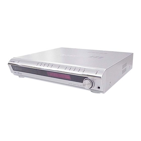
Photo: HCD-DX150
Model Name Using Similar Mechanism
Mechanism Type
Optical Pick-up Name
SPECIFICATIONS
Central/South American models
Stereo mode (rated)
55 W + 55 W (DIN)
Surround mode (reference) music power output
Front: 120 W + 120 W
Center*: 120 W
Surround*: 120 W + 120
W
Subwoofer*: 120 W
Other models:
Stereo mode (rated)
55 W + 55 W (3 ohms at 1
kHz, DIN)
Surround mode (reference) music power output
Front: 133 W + 133 W
(with SS-TS31)
Center*: 133 W
(with SS-CT31)
Surround*: 133 W + 133
W
(with SS-TS31B)
Subwoofer*: 135 W
(with SS-WS31)
DX170
Surround mode (reference) music power output
Front: 143 W + 143 W
(with SS-TS31)
Center*: 143 W
(with SS-CT31)
Surround*: 143 W + 143
W
(with SS-TS31B)
Subwoofer*: 285 W
(with SS-WS32)
HCD-DX150/DX170/
Canadian Model
HCD-DX150/DX170/DX250
Australian Model
DX250
Surround mode (reference) music power output
Depending on the sound field settings and the source,
there may be no sound output.
Inputs
VIDEO/SAT (AUDIO IN) Sensitivity: 250/450 mV
Phones
DVD RECEIVER
DX250
US Model
E Model
HCD-DX150
NEW
CDM81C-DVBU101
KHM-310CAB/C2NP
Front: 143 W + 143 W
(with SS-TS41)
Center*: 143 W
(with SS-CT31)
Surround*: 143 W + 143
W
(with SS-TS31B)
Subwoofer*: 285 W
(with SS-WS32)
Impedance: 50 kilohms
Accepts low-and high-
impedance headphones.
— Continued on next page —
Advertisement
Table of Contents


Need help?
Do you have a question about the HCD-DX170 and is the answer not in the manual?
Questions and answers