Table of Contents
Advertisement
Quick Links
Advertisement
Table of Contents

Subscribe to Our Youtube Channel
Related Manuals for Standard Horizon HX851


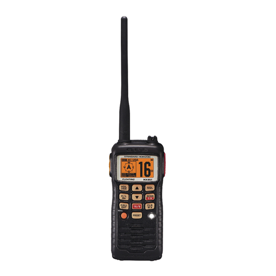
Summary of Contents for Standard Horizon HX851
- Page 1 Floating Marine Transceiver with GPS HX851 SERVICE MANUAL EM031N95C...
-
Page 2: Specifications
Specifications General Frequency Range: TX: 156.025 MHz - 157.425 MHz RX: 156.050 MHz - 163.275MHz Channel Spacing: 25 kHz Frequency Stability: ±10 ppm (–4 °F to +140 °F [–20 °C to +60 °C]) Emission Type: 16K0G3E for Voice, 16K0G2B for DSC 50 Ω... -
Page 3: Exploded View & Miscellaneous Parts
Exploded View & Miscellaneous Parts RA1001800 RA057720A HOLDER (DISTRESS) LIGHT GUIDE (LED) RA0995700 RA040160A RUBBER KNOB (DISTRESS) O RING (3.6X0.8) CP9195010 CP9195012(CE) RA0995600 FRONT PANEL ASSY COVER (DISTRESS) RA046760A RA0999400 O RING (ANT) HOLDER (PTT) RA108700B RA1193300 KNOB SCREW (SP/MIC) RUBBER KNOB (PTT/ORANGE) (Rubber cover) RA1191600... - Page 4 Exploded View & Miscellaneous Parts Note...
- Page 5 Block Diagram...
- Page 6 Block Diagram...
-
Page 7: Circuit Description
Circuit Description 1. Receive Signal Path 3. Squelch Control Incoming RF from the antenna jack is delivered to the When no carrier received, noise at the output of the de- Main Unit and passes through a low-pass filter consist- tector stage in Q1031 (NJM2591V) passes through a ing of coils L1001, L1002, &... -
Page 8: Automatic Transmit Power Control
Circuit Description 4-1 Automatic Transmit Power Control The 12.5 kHz signal from the programmable divider (de- rived from the VCO) and that derived from the refer- Current from the final amplifier Q1009 (RD09MUS2) is ence oscillator are applied to the phase detector section sampled by C1009 and C1020, and rectified by D1003 of Q1026 (LV2105V), which produces a pulsed output (RB751F). -
Page 9: Miscellaneous Circuits
Circuit Description 7. 1050 Hz Weather Alert Decoder A portion of the signal from an FM IF subsystem IC Q1031 (NJM2591V) passes through a low-pass filter Q1037 (2SC4617-R) to the amplifier Q1038 (2SC4617- R). The amplified signal is delivered to the Schmitt In- verter IC Q1016 (SN74LVC3G14DCT) to obtain the weather alert tone pulse. - Page 10 Circuit Description Note...
-
Page 11: Required Test Equipment
Alignment The HX851 has been carefully aligned at the factory for Required Test Equipment the specified performance across the VHF Marine band. RF Signal Generator with calibrated output level at 200 MHz Realignment should therefore not be necessary except in Deviation Meter (linear detector) the event of a component failure. -
Page 12: Before Alignment
PLL Reference Frequency Align- ter the Alignment Mode. ment Mode. Click the left mouse button on the [ Connect ] button of the HX851 Alignment Pro- gram. RF Signal Generator RF Sampling... -
Page 13: Transmitter Power Output
Alignment 01: Transmitter Maximum Output Power 03: Transmitter Power Output (High) Click the left mouse button on the [ 01: Max Power ] Click the left mouse button on the [ 03: High Power ] button. The transceiver now is in the Transmitter button. -
Page 14: Transmitter Modulation
Alignment 05: Transmitter Power Output (Mid1) 07: Transmitter Modulation Click the left mouse button on the [ 05: Mid1 Power ] Set the AF Generator output to 200 mV rms @ 1 kHz button. The transceiver now is in the Transmitter tone. -
Page 15: Squelch Threshold Adjustment
Alignment 08: Squelch Threshold Adjustment 10: CH70 Squelch Threshold Adjustment Set the RF signal generator output to channel fre- Set the RF signal generator output to 156.525 MHz, quency, at a level of –8 dBµ with ±3.0 kHz deviation at a level of –5 dBµ with ±3.0 kHz deviation with a 1 with a 1 kHz audio tone. -
Page 16: Exit From The Alignment Mode
Click the left mouse button on the [ Store and End ] button to save the new setting(s) and turn off the transceiver. Click the left mouse button on the [ Exit Program ] button to close the HX851 Alignment Program. - Page 17 MAIN Unit Circuit Diagram RX: 4.0 V RX: 3.1 V RX: 2.4 V RX: 2.4 V RX: 0.7 V RX: 2.3 V RX: 3.3 V RX: 4.0 V RX: 4.5 V RX: 0.8 V RX: 0.9 V RX: 0.7 V RX: 0.1 V RX: 2.3 V RX: 3.6 V...
- Page 18 MAIN Unit Note...
- Page 19 MAIN Unit Parts Layout (Side A) LM2904PWR CD4066BPWR 2SC4617 (BR) DTC143ZE (E23) UMD5N IMN10 (N10) VMZ6.8NT2L (Q1004) (Q1034) (Q1041, 1046) (Q1027) (Q1013) (D1025) (D1029) LM2902PWR FMMTL618 (Q1003) (Q1019)
- Page 20 MAIN Unit Parts Layout (Side B) UPD78F1167GC BU2502FS SN74LVC3G14DCTR 2SA1774 (FR) 2SC4617 (BR) 3SK294 (UV) RD01MUS1 DTC144TE (96) RT1N441U (N3) S-812C33AUA UMD5N DA221 (K) (Q1032) (Q1030) (Q1006) (Q1021, 1040, (Q1017, 1022, 1023, (Q1018) (Q1015) (Q1035) (Q1014, 1016, 1039) (Q1007) (Q1011, 1012) (D1024, 1026, 1043) 1033, 1037, 1038)
-
Page 21: Main Unit
MAIN Unit Parts List DESCRIPTION VALUE TOL. MFR'S DESIG VXSTD P/N VERS. SIDE LAY ADR PCB with Components CB4300002 CB4300003 EXPORT CB4300004 AUSTRALIA CB4300006 EUROPE CB4300007 Printed Circuit Board FR017870D C 1001 CHIP CAP. 0.001uF GRM155B11H102KA01D K22178809 C 1003 CHIP CAP. 0.1uF GRM155B11A104KA01D K22108802... - Page 22 MAIN Unit Parts List DESCRIPTION VALUE TOL. MFR'S DESIG VXSTD P/N VERS. SIDE LAY ADR C 1081 CHIP CAP. 0.001uF GRM155B11H102KA01D K22178809 C 1082 CHIP CAP. 0.001uF GRM155B11H102KA01D K22178809 C 1083 CHIP CAP. 0.001uF GRM155B11H102KA01D K22178809 C 1084 CHIP CAP. 0.01uF GRM155B11E103KA01D K22148834...
- Page 23 MAIN Unit Parts List DESCRIPTION VALUE TOL. MFR'S DESIG VXSTD P/N VERS. SIDE LAY ADR C 1163 CHIP CAP. GRM188F11A105ZA01D K22105001 C 1164 CHIP CAP. TMK105CJ030C-F K22148207 C 1166 CHIP CAP. GRM188F11A105ZA01D K22105001 C 1167 CHIP CAP. 0.01uF GRM155B11E103KA01D K22148834 C 1168 CHIP CAP.
- Page 24 MAIN Unit Parts List DESCRIPTION VALUE TOL. MFR'S DESIG VXSTD P/N VERS. SIDE LAY ADR C 1242 CHIP CAP. 6.3V GRM155B30J105KE18D K22088803 C 1243 CHIP CAP. 0.1uF GRM155B11A104KA01D K22108802 C 1244 CHIP CAP. 0.1uF GRM155B11A104KA01D K22108802 C 1245 CHIP TA.CAP. 22uF 6.3V TEESVA0J226M8R...
- Page 25 MAIN Unit Parts List DESCRIPTION VALUE TOL. MFR'S DESIG VXSTD P/N VERS. SIDE LAY ADR D 1013 SML-512DWT86 G2071116 D 1014 SML-512DWT86 G2071116 D 1015 SML-512DWT86 G2071116 D 1016 SML-512DWT86 G2071116 D 1017 SML-512DWT86 G2071116 D 1018 SML-512DWT86 G2071116 D 1019 SML-512DWT86 G2071116 D 1020...
- Page 26 MAIN Unit Parts List DESCRIPTION VALUE TOL. MFR'S DESIG VXSTD P/N VERS. SIDE LAY ADR Q 1001 TAR5S33U(TE85L.F) G1094549 Q 1002 TAR5S50U(TE85L.F) G1094097 Q 1003 LM2902PWR G1094009 Q 1004 LM2904PWR G1094010 Q 1005 TAR5S50U(TE85L.F) G1094097 Q 1006 SN74LVC3G14DCTR G1094258 Q 1007 S-812C33AUA-C2N-T2G G1094056 Q 1008...
- Page 27 MAIN Unit Parts List DESCRIPTION VALUE TOL. MFR'S DESIG VXSTD P/N VERS. SIDE LAY ADR R 1014 CHIP RES. 1/16W RMC1/16S 681JTH J24189023 R 1015 CHIP RES. 1/16W RMC1/16S 221JTH J24189017 R 1016 CHIP RES. 2.7k 1/16W RMC1/16S 272JTH J24189030 R 1017 CHIP RES.
- Page 28 MAIN Unit Parts List DESCRIPTION VALUE TOL. MFR'S DESIG VXSTD P/N VERS. SIDE LAY ADR R 1093 CHIP RES. 1/16W RMC1/16S 183JTH J24189040 R 1094 CHIP RES. 1/16W RMC1/16S 183JTH J24189040 R 1095 CHIP RES. 4.7k 1/16W RMC1/16S 472JTH J24189033 R 1096 CHIP RES.
- Page 29 MAIN Unit Parts List DESCRIPTION VALUE TOL. MFR'S DESIG VXSTD P/N VERS. SIDE LAY ADR R 1174 CHIP RES. 3.3k 1/16W RMC1/16S 332JTH J24189031 R 1175 CHIP RES. 330k 1/16W RMC1/16S 334JTH J24189055 R 1176 CHIP RES. 1/16W RMC1/16S 220JTH J24189005 R 1177 CHIP RES.
- Page 30 MAIN Unit Parts List DESCRIPTION VALUE TOL. MFR'S DESIG VXSTD P/N VERS. SIDE LAY ADR R 1251 CHIP RES. 2.2k 1/16W RMC1/16S 222JTH J24189029 R 1252 CHIP RES. 3.3k 1/16W RMC1/16S 332JTH J24189031 R 1253 CHIP RES. 1/16W RMC1/16S 473JTH J24189045 R 1255 CHIP RES.
-
Page 31: Charger Cradle
CD-38 Charger Cradle Exploded View RA0996900 CASE (CHARGER) T9207458 WIRE ASSY CHARGER UNIT : When removing the Charger Unit from the Case, gently pull on the charger unit while pushing the three charging terminals from the outside of the case. ... -
Page 32: Parts Layout
CD-38 Charger Cradle Parts Layout (Side A) (Side B) NJM2904V DTA114EUA 2SC4617 (BR) (Q3001) (Q3009) (Q3004) NJM2360AM DTC114TE (04) RT1N241M (N2) (Q3007) (Q3002, 3005) (Q3003, 3008) - Page 33 CD-38 Charger Cradle Parts List DESCRIPTION VALUE TOL. MFR'S DESIG VXSTD P/N VERS. SIDE LAY ADR Printed Circuit Board AAF94X000 FR0180800 C 3001 CHIP CAP. 0.1uF GRM188B11C104KA01D K22124805 C 3002 CHIP TA.CAP. 10uF TEESVA1C106M8R K78120077 C 3003 CHIP CAP. 0.1uF GRM21BB11E104KA01L K22140811 C 3004...
- Page 34 © 2010 VERTEX STANDARD CO., LTD. All rights reserved. Marine Division of VERTEX STANDARD No portion of this manual US Headquarters may be reproduced 10900 Walker Street, Cypress, CA 90630, U.S.A. without the permission of VERTEX STANDARD CO., LTD.
Need help?
Do you have a question about the HX851 and is the answer not in the manual?
Questions and answers