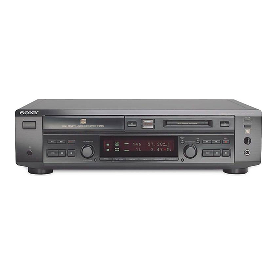
Sony MXD-D40 Service Manual
Compact disc minidisc deck
Hide thumbs
Also See for MXD-D40:
- Operating instructions manual (52 pages) ,
- Limited warranty (1 page)
Table of Contents
Advertisement
SERVICE MANUAL
Ver. 1.2 2005.03
US and foreign patents licensed from Dolby
Laboratories Licensing Corporation.
CD player section
System
Compact Disc digital audio system
Laser
Semiconductor laser (λ = 780 nm)
Emission duration: continuous
Laser output
Less than 44.6 µW*
* This output is the value measured at a
distance of 200 mm from the objective
lens surface on the Optical Pick-up
Block with 7 mm aperture.
Frequency response
5 to 20,000 Hz ±0.5 dB
Signal-to-noise ratio
More than 98 dB
Wow and flutter
Below measurable limit
MD deck section
System
MiniDisc digital audio system
Disc
MiniDisc
Laser
Semiconductor laser (λ = 780 nm)
Emission duration: continuous
Laser output
Less than 44.6 µW*
* This output is the value measured at a
distance of 200 mm from the objective
lens surface on the Optical Pick-up
Block with 7 mm aperture.
Laser diode properties Material: GaAlAs
Revolutions (CLV)
800 rpm to 1,800 rpm
Sony Corporation
9-929-578-13
Audio Group
2005C05-1
Published by Sony Engineering Corporation
© 2005.03
MXD-D40
Photo: Gold type
Model Name Using Similar Mechanism
MD
MD Mechanism Type
Section
Optical Pick-up Name
Model Name Using Similar Mechanism
CD
CD Mechanism Type
Section
Base Unit Name
Optical Pick-up Name
SPECIFICATIONS
Error correction
Sampling frequency
Coding
Modulation system
Number of channels
Frequency response
Signal-to-noise ratio
Wow and flutter
Inputs
Jack type Input
Phono
ANALOG IN
jacks
Square
DIGITAL
optical
OPTICAL IN
connector
jack
COMPACT DISC MINIDISC DECK
US Model
Canadian Model
AEP Model
UK Model
E Model
MXD-D5C
MDM-7X2A
KMS-262A
MXD-D4
CDM55B-21BD53
BU-21BD53
OP Assy (A-MAX.2)
Advanced Cross Interleave Reed
Solomon Code (ACIRC)
44.1 kHz
Adaptive TRansform Acoustic Coding
(ATRAC)/ATRAC 3
EFM (Eight-to-Fourteen Modulation)
2 stereo channels
5 to 20,000 Hz ±0.5 dB
Over 98 dB during playback
Below measurable limit
Rated
Minimum
impedance
input
input
47 kilohms
500 mVrms 125 mVrms
Optical wave
length:
—
—
660 nm
– Continued on next page –
Advertisement
Table of Contents

Related Manuals for Sony MXD-D40


Summary of Contents for Sony MXD-D40
- Page 1 – Continued on next page – Block with 7 mm aperture. Laser diode properties Material: GaAlAs COMPACT DISC MINIDISC DECK Revolutions (CLV) 800 rpm to 1,800 rpm Sony Corporation 9-929-578-13 Audio Group 2005C05-1 Published by Sony Engineering Corporation © 2005.03...
- Page 2 OPERATION. REPLACE THESE COMPONENTS WITH DE FONCTIONNEMENT. NE REMPLACER CES COM- SONY PARTS WHOSE PART NUMBERS APPEAR AS POSANTS QUE PAR DES PIÈCES SONY DONT LES SHOWN IN THIS MANUAL OR IN SUPPLEMENTS PUB- NUMÉROS SONT DONNÉS DANS CE MANUEL OU LISHED BY SONY.
-
Page 3: Self-Diagnosis Function
E0101/LASER NG There ia a problem with the optical pick-up. , The optical pick-up may have failed. Consult your nearest Sony dealer. PROCEDURE FOR USING THE SELF-DIAGNOSIS FUNCTION (ERROR HISTORY DISPLAY MODE) Note: Perform the self-diagnosis function in the “error history display mode” in the test mode. The following describes the least required procedure. Be [MENU/NO] careful not to enter other modes by mistake. - Page 4 MXD-D40 ITEMS OF ERROR HISTORY MODE ITEMS AND CONTENTS Selecting the Test Mode Display Details of History op rec tm Cumulative recording time is displayed. When cumulative recording time is over 1 minute, the hour and minute are displayed as they are.
- Page 5 MXD-D40 Table of Error Codes Error Code Details of Error Loading failed Loading switch combination is illegal Head of PTOC could not be read within the specified time Head of PTOC could be read but its content is erroneous Access to UTOC could not be made within the...
-
Page 6: Table Of Contents
MXD-D40 TABLE OF CONTENTS SELF-DIAGNOSIS FUNCTION 6-22. Printed Wiring Board – HP Board – ....... 70 ......3 6-23. Schematic Diagram – HP Board – ........70 6-24. IC Pin Function Description ........... 72 SERVICING NOTES ..........8 EXPLODED VIEWS GENERAL .............. - Page 7 MXD-D40 SAFETY CHECK-OUT CAUTION After correcting the original service problem, perform the follow- Danger of explosion if battery is incorrectly replaced. ing safety check before releasing the set to the customer: Replace only with the same or equivalent type recommended by Check the antenna terminals, metal trim, “metallized”...
-
Page 8: Servicing Notes
MXD-D40 SECTION 1 SERVICING NOTES CLEANING OBJECTIVE LENS OF OPTICAL PICK-UP NOTES ON HANDLING THE OPTICAL PICK-UP • In cleaning the objective lens of optical pick-up, be sure the BLOCK OR BASE UNIT following below. The laser diode in the optical pick-up block may suffer electro- static break-down because of the potential difference generated 1. - Page 9 MXD-D40 MD SECTION JIG FOR CHECKING BD (MD) BOARD WAVEFORM The special jig (J-2501-196-A) is useful for checking the waveform of the BD (MD) board. The names of terminals and the checking items to be performed are shown as follows.
- Page 10 MXD-D40 IOP DATA RECORDING AND DISPLAY WHEN OPTICAL PICK-UP AND NON-VOLATILE MEMORY (IC195 OF BD (MD) BOARD) ARE REPLACED The IOP value labeled on the optical pick-up can be recorded in the non-volatile memory. By recording the value, it will eliminate the need to look at the value on the optical pick-up label.
- Page 11 MXD-D40 CHECKS PRIOR TO PARTS REPLACEMENT AND ADJUSTMENTS IN MD Before performing repairs, perform the following checks to determine the faulty locations up to a certain extent. Details of the procedures are described in “5 Electrical Adjustments”. Criteria for Determination...
- Page 12 MXD-D40 SERVICE MODE This set provides various modes for the service. Enter the service mode through the procedure given below, and select the desired mode. Procedure: [YES] 1. Press the (CD), (MD) and buttons at the same time. 2. Press the (MD) knob and (MD) button to display “...
- Page 13 MXD-D40 Microcomputer Version Display Procedure: 1. Enter the service mode, then turn (MD) knob to display “<Version> 1”, and press the (MD). 2. The CD microcomputer version is displayed, and then press the (MD) knob, and the MD microcomputer version and the display microcomputer version will be displayed.
- Page 14 MXD-D40 RETRY CAUSE DISPLAY MODE IN MD • In this test mode, the causes for retry of the unit during recording can be displayed on the fluorescent indicator tube. During playback, the “track mode” for obtaining track information will be set.
- Page 15 MXD-D40 Reading the Retry Cause Display Higher Bits Lower Bits Hexa- Details Hexadecimal decimal When 0 When 1 b7 b6 b5 b4 b3 b2 b1 b0 Binary Emphasis OFF Emphasis ON Monaural Stereo This is 2-bit display. Normally 01. 01:Normal audio. Others:Invalid...
- Page 16 MXD-D40 CD SECTION • In checking the CD block and MAIN board, prepare jig. • In checking the CD block, prepare jig (extension cable J-2501-075-A) to connect the BD (CD) board (CN101) and MAIN board (CN302). • In checking the MAIN board, prepare jig (extension cable J-2501-094-A) to connect the MAIN board (CN305) and DISPLAY board (CN951).
- Page 17 MXD-D40 Table 2: CD-TEXT TEST DISC Recorded Contents and Display (In this unit, some special characters cannot be displayed. This is not a fault) TRACK Recorded contents Display T All the same ! ” # $ % & ´ (21h to 27h)1kHz 0dB L&R T All the same + , –...
-
Page 18: General
MXD-D40 SECTION 2 This section is extracted from instruction manual. GENERAL Front view Rear view 5 6 78 9 q; qa 2 3 4 1 STANDBY indicator 1 ANALOG IN jack 2 ?/1 (power) button 2 ANALOG OUT jack 3 DIGITAL OPTICAL IN terminal... -
Page 19: Disassembly
MXD-D40 SECTION 3 DISASSEMBLY • This set can be disassembled in the order shown below. 3-1. DISASSEMBLY FLOW Note: The process described in can be performed in any order. Note: Without completing the process described in , the next process can not be performed. -
Page 20: Loading Panel
MXD-D40 Note: Follow the disassembly procedure in the numerical order given. 3-2. LOADING PANEL 4 loading panel 3 two claws 3-3. CASE 1 two screws (case3 TP2) 1 two screws (case3 TP2) 2 case 1 two screws (case3 TP2) -
Page 21: Front Panel Assy
MXD-D40 3-4. FRONT PANEL ASSY 1 wire (flat type) (18 core) (CN305) 4 three screws (BVTT3 × 6) 2 connector (CN300) 5 two lugs 6 claw 7 front panel assy 6 claw 3 six screws (BVTT3 × 6) 3-5. MAIN BOARD... -
Page 22: Md Mechanism Deck (Mdm-7X2A)
MXD-D40 3-6. MD MECHANISM DECK (MDM-7X2A) 4 four screws (BVTTWH M3) 5 MD mechanism deck 1 wire (flat type) (17core) (MDM-7X2A) (CN303) 2 two screws (BVTT 3 × 6) 1 wire (flat type) (27core) (CN304) 3 two lugs 3-7. BD (MD) BOARD, OVER WRITE HEAD (HR901) -
Page 23: Holder Assy
MXD-D40 3-8. HOLDER ASSY 2 claw 6 holder assy 4 boss 4 boss 1 tension spring (holder) 3-9. LOADING MOTOR ASSY (M103) 1 belt (loading) 2 two screws × (PWH1.7 2.5) 3 loading motor assy (M103) -
Page 24: Sled Motor Assy (M102)
MXD-D40 3-10. SLED MOTOR ASSY (M102) 5 With holding the claw, 4 slider (EJ) slide the slider fully in the direction of arrow A . 8 lever (head) 6 slider 2 guide (L) 1 two screws × 9 two screws 7 lever (CHG) ×... -
Page 25: Spindle Motor Assy (M101)
MXD-D40 3-12. SPINDLE MOTOR ASSY (M101) 2 spindle motor assy (M101) 1 three screws (M1.7) 3-13. CD MECHANISM DECK (CDM55B-21BD53) 6 CD mechanism deck × 5 screw (BVTT3 (CDM55B-21BD53) 1 wire (flat type) (21 core) (CN302) 2 connector (CN301) 3 screw ×... -
Page 26: Holder (Bu) Assy
MXD-D40 3-14. HOLDER (BU) ASSY 2 floating screw (PTPWH M2.6) 4 holder (BU) assy 1 Rotate the lever (SW) in the direction of the arrow A . 3-15. BU-21BD53, HOLDER (55-BU21) 1 three floating screws (DIA. 12) 2 floating screw (PTPWH M2.6) -
Page 27: Tray, Loading Board
MXD-D40 3-16. TRAY, LOADING BOARD 2 belt (CDM55) claw 1 Rotate the gear (B) in the direction of arrow A. 3 Pull the tray pushing claw. 5 LOADING board 4 two screws (BTP2.6 × 8) 3-17. CAM (CDM55) 3 spacer (55) -
Page 28: Test Mode
MXD-D40 SECTION 4 TEST MODE MD SECTION Note: MD always plays double speed. 1. PRECAUTIONS FOR USE OF TEST MODE • As loading related operations will be performed regardless of the test mode operations being performed, be sure to check that the disc is stopped before setting and removing it. -
Page 29: Selecting The Test Mode
MXD-D40 5. SELECTING THE TEST MODE There are 26 types of test modes as shown below. The groups can be switched by turning the (MD) knob. After selecting [YES] the group to be used, press the button. After setting a certain group, turn the (MD) knob switches between these modes. - Page 30 MXD-D40 5-1. Operating the Continuous Playback Mode 1. Entering the continuous playback mode (1) Set the disc in the unit. (Whichever recordable discs or discs for playback only are available) (2) Turn the (MD) knob and display “CPLAY2MODE” (C36). [YES] (3) Press the button to change the display to “CPLAY2MID”.
- Page 31 MXD-D40 7. TEST MODE DISPLAYS [DISPLAY] Each time the button is pressed, the display changes in the following order. When CPLAY and CREC are started, the display will forcibly be switched to the error rate display as the initial mode.
- Page 32 MXD-D40 8. AUTOMATIC SELF-DIAGNOSIS FUNCTION This test mode performs CREC and CPLAY automatically for mainly checking the characteristics of the optical pick-up. To perform this test mode, the laser power must first be checked. Perform AUTO CHECK after the laser power check and Iop check.
- Page 33 MXD-D40 CD SECTION Set the CD test mode when performing confirmations (refer to page 12). After completing confirmation, release the CD test mode. 1. COMMAND TRANSFER MENU Procedure: (1) Enter the test mode, then rotate (MD) knob to display “0> COMMAND”, and press the (MD) knob.
-
Page 34: Electrical Adjustments Md Section
MXD-D40 SECTION 5 ELECTRICAL ADJUSTMENTS MD SECTION Note: MD always plays double speed. 1. PARTS REPLACEMENT AND ADJUSTMENT If malfunctions caused by Optical pick-up such as sound skipping are suspected, follow the following check. Check before replacement Start 6-2. Laser Power Check (See page 37) 6-3. - Page 35 MXD-D40 Adjustment flow • Abbreviation Start OP: optical pick-up After turning off and then on the power, initialize the EEPROM Replace IC195 For details, refer to 10. WHEN MEMORY NG IS DISPLAYED (See page 32) INITIAL SETTING OF ADJUSTMENT VALUE...
- Page 36 MXD-D40 2. PRECAUTIONS FOR CHECKING LASER DIODE EMISSION To check the emission of the laser diode during adjustments, never view directly from the top as this may lose your eye-sight. 3. PRECAUTIONS FOR USE OF OPTICAL PICK- UP (KMS-262A) As the laser diode in the optical pick-up is easily damaged by static electricity, solder the laser tap of the flexible board when using it.
- Page 37 MXD-D40 5. USING THE CONTINUOUSLY RECORDED DISC Checking Procedure: 1. Set the laser power meter on the objective lens of the optical * This disc is used in focus bias adjustment and error rate check. pick-up. (When it cannot be set properly, press the m button The following describes how to create a continuous recording or M button to move the optical pick-up.)
- Page 38 MXD-D40 6-6. Traverse Check 6-4. Auto Check This test mode performs CREC and CPLAY automatically for mainly checking the characteristics of the optical pick-up. To Note 1:Data will be erased during MO reading if a recorded disc is used in this adjustment.
- Page 39 MXD-D40 [YES] 9. Press the button to display “EFB = MO-P”. 6-7. Focus Bias Check Then, the optical pick-up moves to the pit area automatically Change the focus bias and check the focus tolerance amount. and servo is imposed. Checking Procedure: 10.
- Page 40 MXD-D40 7. INITIAL SETTING OF ADJUSTMENT VALUE 9. TEMPERATURE COMPENSATION OFFSET ADJUSTMENT Note: Save the temperature data at that time in the non-volatile memory Mode which sets the adjustment results recorded in the non-volatile as 25 ˚C reference data. memory to the initial setting value. However the results of the tempera-...
- Page 41 MXD-D40 6. Turn the (MD) knob so that the reading of 4. After “Complete!” is displayed momentarily, the display changes [YES] the laser power meter becomes 8.2 to 8.6 mW, press the to “Iop 7.0 mW”. [YES] button to save it.
- Page 42 MXD-D40 [YES] 8. Turn the (MD) knob so that the waveform 18. Press the button, display “EFB = SAVE” for a mo- of the oscilloscope becomes the specified value. ment and save the adjustment results in the non-volatile (When the (MD) knob is turned, the memory.
- Page 43 MXD-D40 14. ERROR RATE CHECK 16. AUTO GAIN CONTROL OUTPUT LEVEL ADJUSTMENT 14-1. CD Error Rate Check Be sure to perform this adjustment when the optical pick-up is Checking Procedure: replaced. 1. Load the check disc (MD) TDYS-1. If the adjustment results becomes “Adjust NG!”, the optical pick- 2.
- Page 44 MXD-D40 Adjustment and checking Loacation: – BD (MD) BOARD (Side A) – D101 CN101 – BD (MD) BOARD (Side B) – IC101 CN105 1. I+3V 2. IOP 3. GND 4. TE 5. FE 6. VC 7. RF IC151 IC190 Note: It is useful to use the jig for checking the waveform. (Refer to Ser-...
-
Page 45: Cd Section
MXD-D40 Note: A clear RF signal waveform means that the shape “◊” can be clearly CD SECTION distinguished at the center of the waveform. Note: RF signal waveform 1. CD Block is basically designed to operate without adjustment. There- VOLT/DIV: 200 mV fore, check each item in order given. - Page 46 MXD-D40 Checking Location: Voltage Adjustment When replacing the base unit (BU-21BD53), mounted MAIN board – BD (CD) BOARD (Side B) – and IC506, R550, R551, or RV500 on the MAIN board, perform the adjustment with the following procedure. Connection: digital voltmeter...
-
Page 47: Diagrams
MXD-D40 SECTION 6 DIAGRAMS 6-1. BLOCK DIAGRAM – MD SERVO Section – DIGITAL SIGNAL PROCESSOR, EFM/ACIRC ENCODER/DECODER, SHOCK PROOF MEMORY CONTROLLER, ATRAC ENCODER/DECODER OVER WRITE EFMO ADDT IC151 (1/2) HEAD DRIVE DATAI ADDT IC181, Q181, 182 SAMPLING (Page 48) RATE... -
Page 48: Block Diagram - Main Section
MXD-D40 6-2. BLOCK DIAGRAM – MAIN Section – J300 DATAO ADDT VINL LINE LRCK DIGITAL DECIMATION (Page 47) CANCELLATION CONVERTER INTERFACE FILTER FILTER BLOCK VINR IC305 RESET PWON ANALOG SWITCH CLOCK Q301 SCLK CONTROL A/D CONVERTER IC301 D/A CONVERTER RV301... -
Page 49: Block Diagram - Display/Power Supply Section
MXD-D40 6-3. BLOCK DIAGRAM – DISPLAY/POWER SUPPLY Section – FL/LED DRIVE IC751 REMOTE CONTROL RECEIVER SIRCS S01 – S35 S731 – 736 IC781 KEY2 FLCLK FLUORESCENT G02 – G23 INDICATOR TUBE FLWITE FL751 S741 – 746, FL DRIVE S791 COM01... -
Page 50: Note For Printed Wiring Boards And Schematic Diagrams
MXD-D40 6-4. NOTE FOR PRINTED WIRING BOARDS AND SCHEMATIC DIAGRAMS • Circuit Boards Location (In addition to this, the necessary note is printed in each block) Note on Printed Wiring Board: Note on Schematic Diagram: • All capacitors are in µF unless otherwise noted. pF: µµF •... - Page 51 MXD-D40 • IC Block Diagrams IC141 BH6519FS-E2 – BD (MD) Board – IC101 CXA2523AR 43 42 INTERFACE INTERFACE USROP – RF AGC – CHARGE USRC PREDRIVE PREDRIVE RFA1 PUMP. BPF3T RFA2 RFA3 PEAK3T – HLPT PREDRIVE PREDRIVE –1 – –...
-
Page 52: Printed Wiring Board - Bd (Cd) Board
MXD-D40 6-5. PRINTED WIRING BOARD – BD (CD) Board – • See page 50 for Circuit Boards Location. BD(CD) BOARD (SIDE A) BD(CD) BOARD (SIDE B) (SPINDLE) S101 (LIMIT) (VC) (FE) (TE) (RFDC) MAIN BOARD CN302 (Page 58) C1 C2... -
Page 53: Schematic Diagram - Bd (Cd) Board
MXD-D40 6-6. SCHEMATIC DIAGRAM – BD (CD) Board – • See page 57 for Waveforms. (Page The components identified by mark 0 or dotted Les composants identifiés par une marque 0 sont line with mark 0 are critical for safety. -
Page 54: Schematic Diagram - Bd (Md) Board (1/2)
MXD-D40 6-7. SCHEMATIC DIAGRAM – BD (MD) Board (1/2) – • • See page 57 for Waveforms. See page 51 for IC Block Diagrams. (Page 55) (Page 55) (Page 55) Note on Schematic Diagram: • Voltages and waveforms are dc with respect to ground under no-signal conditions. -
Page 55: Schematic Diagram - Bd (Md) Board (2/2)
MXD-D40 6-8. SCHEMATIC DIAGRAM – BD (MD) Board (2/2) – • • See page 57 for Waveforms. See page 51 for IC Block Diagram. (Page 54) (Page 60) (Page 54) (Page 62) (Page 54) Note on Schematic Diagram: • Voltages and waveforms are dc with respect to ground under no-signal conditions. -
Page 56: Printed Wiring Board - Bd (Md) Board
MXD-D40 6-9. PRINTED WIRING BOARD – BD (MD) Board – • See page 50 for Circuit Boards Location. OPTICAL PICK-UP FLEXIBLE BOARD BLOCK (KMS-262A) 1-678-514- BD(MD) BOARD (SIDE B) BD(MD) BOARD (SIDE A) S102-2 PROTECT M103 DETECT –1 (LOADING) S102-1 REFLECT –2... - Page 57 MXD-D40 • Waveforms – BD (MD) Board – – BD (CD) Board – – MAIN Board – – DISPLAY Board – 1 IC101 wg (MDP) (CD PLAY mode) 6 IC101 us (XTAO) 1 IC101 1 (I), 2 (J) (MD PLAY mode)
-
Page 58: Printed Wiring Board - Main Board (Side A)
MXD-D40 6-10. PRINTED WIRING BOARD – MAIN Board (Side A) – • See page 50 for Circuit Boards Location. (Page 64) DISPLAY BOARD CN701 MAIN BOARD (SIDE A) (US, CND) (AEP, UK) (SP) (FOR CHECK) (BU +5V) (FOR CHECK) (GND) -
Page 59: Printed Wiring Boards - Main (Side B)/Loading Boards
MXD-D40 6-11. PRINTED WIRING BOARDS – MAIN (Side B)/LOADING Boards – • See page 50 for Circuit Boards Location. J302 PC LINK J300 ANALOG (SHORT SOCKET) DIGITAL OPTICAL MAIN BOARD (SIDE B) (EXCEPT SINGAPORE) TRANS BOARD CN650 (Page 66) TRANS(SP) BOARD... -
Page 60: Schematic Diagram - Main Board (1/4)
MXD-D40 6-12. SCHEMATIC DIAGRAM – MAIN Board (1/4) – • See page 57 for Waveform. • See page 70 for IC Block Diagram. SPDIF BUFFER (Page 61) (Page 55) (Page 63) Note on Schematic Diagram: • Voltages and waveforms are dc with respect to ground (Page 62) under no-signal conditions. -
Page 61: Schematic Diagram - Main (2/4)/Loading Boards
MXD-D40 6-13. SCHEMATIC DIAGRAM – MAIN (2/4)/LOADING Boards – • • See page 57 for Waveform. See page 70 for IC Block Diagram. (Page 53) (Page 60) (Page 65) (Page 62) Note on Schematic Diagram: (Page 63) • Voltages and waveforms are dc with respect to ground under no-signal conditions. -
Page 62: Schematic Diagram - Main Board (3/4)
MXD-D40 6-14. SCHEMATIC DIAGRAM – MAIN Board (3/4) – • See page 70 for IC Block Diagrams. (Page 60) (Page 61) (Page 55) (Page 70) (Page 63) Note on Schematic Diagram: The components identified by mark 0 or dotted Les composants identifiés par une marque 0 sont •... -
Page 63: Schematic Diagram - Main Board (4/4)
MXD-D40 6-15. SCHEMATIC DIAGRAM – MAIN Board (4/4) – • See page 70 for IC Block Diagrams. (Page 61) (Page 60) (Page 67) (Page (Page 69) (Page 67) (Page 69) Note on Schematic Diagram: • Voltages and waveforms are dc with respect to ground Note: Be sure to execute the Voltage Adjustment on page 46, whenever the asterisked parts (IC506, R550, R551, RV500), mounted under no-signal conditions. -
Page 64: Printed Wiring Boards - Display/Lp Led/Pw Sw Boards
MXD-D40 6-16. PRINTED WIRING BOARDS – DISPLAY/LP LED/PW SW Boards – • See page 50 for Circuit Boards Location. (Page 58) (MD) (HD) • Semiconductor Location Ref. No. Location D751 D752 IC751 Q751 Q752 Q753 B-10 Q754 B-10 Q791 B-10 There are a few cases that the part isn't mounted in model is printed on diagrams. -
Page 65: Schematic Diagram - Display/Lp Led/Pw Sw Boards
MXD-D40 6-17. SCHEMATIC DIAGRAM – DISPLAY/LP LED/PW SW Boards – • See page 57 for Waveform. (Page 61) Note on Schematic Diagram: • Voltages and waveforms are dc with respect to ground under no-signal conditions. no mark : MD, CD STOP... -
Page 66: Printed Wiring Board - Trans Board (Except Singapore)
MXD-D40 6-18. PRINTED WIRING BOARD – TRANS Board (Except Singapore) – • See page 50 for Circuit Boards Location. (Page 59) SUB POWER TRANSFORMER (Page 59) There are a few cases that the part isn't mounted in model is printed on diagrams. -
Page 67: Schematic Diagram - Trans Board (Except Singapore)
MXD-D40 6-19. SCHEMATIC DIAGRAM – TRANS Board (Except Singapore) – (Page 63) (Page 63) The components identified by mark 0 or dotted Les composants identifiés par une marque 0 sont line with mark 0 are critical for safety. critiques pour la sécurité. Ne les remplacer que Replace only with part number specified. -
Page 68: Printed Wiring Boards - Trans (Sp)/Lf Boards (Singapore)
MXD-D40 6-20. PRINTED WIRING BOARDS – TRANS (SP)/LF Boards (Singapore) – • See page 50 for Circuit Boards Location. (Page 59) SUB TRANSFORMER (Page 59) There are a few cases that the part isn't mounted in model is printed on diagrams. -
Page 69: Schematic Diagram - Trans (Sp)/Lf Boards (Singapore)
MXD-D40 6-21. SCHEMATIC DIAGRAM – TRANS (SP)/LF Boards (Singapore) – (Page 63) (Page 63) The components identified by mark 0 or dotted Les composants identifiés par une marque 0 sont line with mark 0 are critical for safety. critiques pour la sécurité. Ne les remplacer que Replace only with part number specified. -
Page 70: Printed Wiring Board - Hp Board
MXD-D40 6-22. PRINTED WIRING BOARD – HP Board – • • IC Block Diagrams See page 50 for Circuit Boards Location. – MAIN Board – IC300 µDA1350AH 41 40 39 38 37 36 RESET BCKO VDDD (C) VDDA (PLL) VSSD... - Page 71 MXD-D40 IC500 LA5643 IC506 BA00AST-V5 REFERENCE – VOLTAGE – STBY ANA5 – SYS3.3 – – 3.3V B.BAK – DELAY P. DOWN CIRCUIT – DELAY S. RESET CIRCUIT VREF IC504 M5293L REFERENCE VOLTAGE REFERENCE – ON/OFF VOLTAGE OVERHEAT OVERCURRENT PROTECTION LIMITTER...
-
Page 72: Ic Pin Function Description
MXD-D40 6-24. IC PIN FUNCTION DESCRIPTION • BD (MD) BOARD IC101 CXA2523AR (RF AMP, FOCUS/TRACKING ERROR AMP) Pin No. Pin Name Description I-V converted RF signal I input from the optical pick-up block detector I-V converted RF signal J input from the optical pick-up block detector Middle point voltage (+1.65V) generation output terminal... - Page 73 MXD-D40 • BD (MD) BOARD IC151 CXD2662R (DIGITAL SIGNAL PROCESSOR, DIGITAL SERVO PROCESSOR, EFM/ACIRC ENCODER/DECODER, SHOCK PROOF MEMORY CONTROLLER, ATRAC ENCODER/DECODER) Pin No. Pin Name Description Focus OK signal output terminal “H” is output when focus is on (“L”: NG)
- Page 74 MXD-D40 Pin No. Pin Name Description XCAS Column address strobe signal output to the D-RAM (IC152) “L” active Address signal output to the D-RAM (IC152) XRAS Row address strobe signal output to the D-RAM (IC152) “L” active Write enable signal output to the D-RAM (IC152) “L” active...
- Page 75 MXD-D40 Pin No. Pin Name Description FRDR Focus servo drive PWM signal (–) output to the BH6511FS (IC141) Clock signal (176.4 kHz) output terminal (X’tal system) Not used (open) SRDR Sled servo drive PWM signal (–) output to the BH6511FS (IC141)
- Page 76 MXD-D40 • MAIN BOARD IC800 M30624MGA-A54FP (SYSTEM CONTROLLER (CD MECHANISM CONTROLLER)) Pin No. Pin Name Description CD-DATA Serial data output to the CD block CD-CLK Serial data transfer clock signal output to the CD block Serial data latch pulse signal output to the CD block...
- Page 77 MXD-D40 Pin No. Pin Name Description SPNDL_MUTE Spindle motor muting control signal output to the CD block — Not used (fixed at “H” in this set) 47 to 51 — Not used (open) LED_RECMODE LED on/off control signal output terminal Not used (open)
- Page 78 MXD-D40 Pin No. Pin Name Description Detection input from the disc in detect sensor on the CD mechanism block DSENSE “H”: disc detected Not used (open) Detection input from the CD tray door open/close detect switch input terminal PRTC_SW “L”: when CD lid is open, “H”: when CD lid is close Not used (open)
- Page 79 MXD-D40 • MAIN BOARD IC801 M30803MG (MD MECHANISM CONTROLLER) Pin No. Pin Name Description 1, 2 Not used (open) LEVEL_L L-ch level output to the CD mechanism controller (IC800) LEVEL_R R-ch level output to the CD mechanism controller (IC800) 5 to 7...
- Page 80 MXD-D40 Pin No. Pin Name Description PLAY-SW Detection input from the playback position detect switch (S104) “L” active D.RESET Reset signal output to the CXD2662R (IC151) and BH6511FS (IC152) “L”: reset REC-SW Detection input from the recording position detect switch (S105) “L” active...
- Page 81 MXD-D40 Pin No. Pin Name Description 81 to 84 Not used (open) 85 to 88 TP1-4 Not used (open) Optical pick-up voltage input from the automatic power control circuit 90 to 95 Not used (open) AVSS — Ground terminal (for analog system )
-
Page 82: Exploded Views
MXD-D40 SECTION 7 EXPLODED VIEWS NOTE: • -XX and -X mean standardized parts, so they • Items marked “*” are not stocked since they The components identified by mark 0 or dotted line with mark may have some difference from the original are seldom required for routine service. -
Page 83: Front Panel Section
MXD-D40 7-2. FRONT PANEL SECTION not supplied not supplied supplied with RV301 not supplied supplied with J301 Ref. No. Part No. Description Remark Ref. No. Part No. Description Remark 4-220-710-01 PLATE, INDICATION 4-950-189-01 KNOB (A) (VOL) (BLACK) 4-996-687-41 KNOB (AMS) (GOLD) -
Page 84: Chassis Section
MXD-D40 7-3. CHASSIS SECTION T601, T651 Singapore not supplied supplied not supplied supplied supplied supplied supplied The components identified by Les composants identifiés par une mark 0 or dotted line with mark marque 0 sont critiquens pour la 0 are critical for safety. -
Page 85: Md Mechanism Deck Section-1 (Mdx-7X2A)
MXD-D40 Ver. 1.2 7-4. MD MECHANISM DECK SECTION-1 (MDM-7X2A) Ref. No. Part No. Description Remark Ref. No. Part No. Description Remark * 301 4-996-267-01 BASE (BU-D) 4-227-012-01 SPRING (HOLDER), TENSION 4-231-319-01 SCREW (2X6) CZN, +B (P) TRI 4-227-019-02 PLATE (HOLDER), RETAINER... -
Page 86: Md Mechanism Deck Section-2 (Mdx-7X2A)
MXD-D40 7-5. MD MECHANISM DECK SECTION-2 (MDM-7X2A) HR901 S102 M101 M102 The components identified by mark 0 or dotted line with mark M103 0 are critical for safety. Replace only with part number specified. Les composants identifiés par une marque 0 sont critiquens pour la not supplied sécurité. -
Page 87: Cd Mechanism Deck Section (Cdm55B-21Bd53)
MXD-D40 Ver. 1.1 7-6. CD MECHANISM DECK SECTION (CDM55B-21BD53) M702 The components identified by mark 0 or dotted line with mark 0 are critical for safety. Replace only with part number specified. Les composants identifiés par une marque 0 sont critiquens pour la sécurité. -
Page 88: Electrical Parts List
MXD-D40 SECTION 8 BD (MD) ELECTRICAL PARTS LIST NOTE: • Due to standardization, replacements in the • Items marked “*” are not stocked since they The components identified by mark 0 or dotted line with mark parts list may be different from the parts speci- are seldom required for routine service. - Page 89 MXD-D40 BD (MD) Ref. No. Part No. Description Remark Ref. No. Part No. Description Remark IC151 8-752-404-64 IC CXD2662R R110 1-216-845-11 METAL CHIP 100K 1/16W IC152 8-759-599-51 IC MSM51V17400D-50TS-K R111 1-216-833-11 METAL CHIP 1/16W IC181 8-759-481-17 IC MC74ACT08DTR2 R112 1-216-829-11 METAL CHIP 4.7K...
- Page 90 MXD-D40 BD (MD) DISPLAY Ref. No. Part No. Description Remark Ref. No. Part No. Description Remark S105 1-771-955-21 SWITCH, PUSH (1 KEY) (REC POSITION) R704 1-249-417-11 CARBON 1/4W R705 1-249-419-11 CARBON 1.5K 1/4W < VIBRATOR > R706 1-249-421-11 CARBON 2.2K...
- Page 91 MXD-D40 DISPLAY LOADING LP LED MAIN Ref. No. Part No. Description Remark Ref. No. Part No. Description Remark S734 1-762-875-21 SWITCH, KEYBOARD (HIGH CD SYNCHRO) 1-674-336-21 LOADING BOARD ************** S735 1-762-875-21 SWITCH, KEYBOARD (NORMAL CD SYNCHRO) S736 1-762-875-21 SWITCH, KEYBOARD (A OPEN/CLOSE) <...
- Page 92 MXD-D40 MAIN Ref. No. Part No. Description Remark Ref. No. Part No. Description Remark C309 1-126-935-11 ELECT 470uF C502 1-165-319-11 CERAMIC CHIP 0.1uF C310 1-165-319-11 CERAMIC CHIP 0.1uF C311 1-163-227-11 CERAMIC CHIP 10PF 0.5PF C504 1-115-364-11 ELECT 22000uF C313 1-165-319-11 CERAMIC CHIP 0.1uF...
- Page 93 MXD-D40 MAIN Ref. No. Part No. Description Remark Ref. No. Part No. Description Remark C818 1-165-319-11 CERAMIC CHIP 0.1uF C819 1-104-665-11 ELECT 100uF < GROUND TERMINAL > C820 1-163-251-11 CERAMIC CHIP 100PF C821 1-163-251-11 CERAMIC CHIP 100PF EP300 1-537-771-21 TERMINAL BOARD, GROUND...
- Page 94 MXD-D40 MAIN Ref. No. Part No. Description Remark Ref. No. Part No. Description Remark Q300 8-729-424-08 TRANSISTOR UN2111 R315 1-216-073-00 METAL CHIP 1/10W 0 R317 1-217-637-00 FUSIBLE 1/4W Q301 8-729-421-22 TRANSISTOR UN2211 R320 1-216-025-11 RES-CHIP 1/10W Q302 8-729-424-08 TRANSISTOR UN2111...
- Page 95 MXD-D40 MAIN TRANS TRANS (SP) PW SW Ref. No. Part No. Description Remark Ref. No. Part No. Description Remark R871 1-216-025-11 RES-CHIP 1/10W < RELAY > R872 1-216-025-11 RES-CHIP 1/10W 0 RY600 1-755-299-11 RELAY R873 1-216-025-11 RES-CHIP 1/10W < SWITCH >...
- Page 96 MXD-D40 Ref. No. Part No. Description Remark Ref. No. Part No. Description Remark M103 A-4672-975-A MOTOR ASSY, LOADING (for MD) M702 A-4672-771-A MOTOR (LD) ASSY (LOADING) (for CD) S102 1-771-957-11 SWITCH, PUSH (2 KEY) (REFLECT RATE DETECT, PROTECT DETECT) 0 T601...
- Page 97 MXD-D40 MEMO...
- Page 98 MXD-D40 REVISION HISTORY Clicking the version allows you to jump to the revised page. Also, clicking the version at the upper right on the revised page allows you to jump to the next revised page. Ver. Date Description of Revision 2001.03...
Need help?
Do you have a question about the MXD-D40 and is the answer not in the manual?
Questions and answers