Sony CDX-M50IP Service Manual
Fm/am compact disc player and fm/mw/lw compact disc player
Hide thumbs
Also See for CDX-M50IP:
- Specifications (3 pages) ,
- Operating instructions manual (148 pages) ,
- Installation/connections (2 pages)
Table of Contents
Advertisement
CDX-M50IP/MR50IP
SERVICE MANUAL
Ver. 1.0 2007. 08
• The tuner and CD sections have no adjustments.
AUDIO POWER SPECIFICATIONS (US model)
POWER OUTPUT AND TOTAL HARMONIC DISTORTION
23.2 watts per channel minimum continuous average power into
4 ohms, 4 channels driven from 20 Hz to 20 kHz with no more
than 5% total harmonic distortion.
CD player section
Signal-to-noise ratio
120 dB
Frequency response
10 – 20,000 Hz
Wow and flutter
Below measurable limit
Tuner section
FM
Tuning range
CDX-M50IP:
87.5 – 108.0 MHz (at 50 kHz step)
87.5 – 107.9 MHz (at 200 kHz step)
CDX-MR50IP:
87.5 – 108.0 MHz
FM tuning interval
CDX-M50IP:
50 kHz/200 kHz switchable
Antenna (aerial) terminal
External antenna (aerial) connector
Intermediate frequency 10.7 MHz/450 kHz
Usable sensitivity
9 dBf
Sony Corporation
9-887-817-01
eVehicle Division
2007H04-1
Published by Sony Techno Create Corporation
© 2007. 08
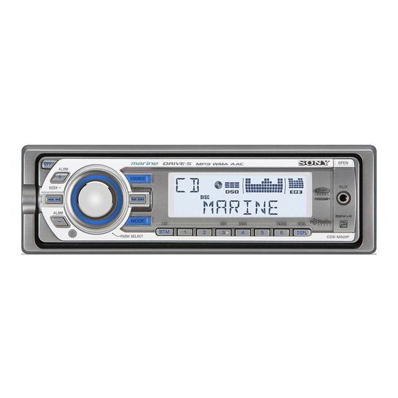
Photo: CDX-M50IP
Model Name Using Similar Mechanism
CD Drive Mechanism Type
Optical Pick-up Name
SPECIFICATIONS
Selectivity
Signal-to-noise ratio
Harmonic distortion at 1 kHz
Separation
Frequency response
AM (CDX-M50IP)
Tuning range
AM tuning interval
Antenna (aerial) terminal
Intermediate frequency 10.7 MHz/450 kHz
Sensitivity
FM/AM COMPACT DISC PLAYER
FM/MW/LW COMPACT DISC PLAYER
US Model
CDX-M50IP
AEP Model
UK Model
CDX-MR50IP
NEW
MG-101FC-188//Q
DAX-25A
75 dB at 400 kHz
67 dB (stereo), 69 dB (mono)
0.5% (stereo), 0.3% (mono)
35 dB at 1 kHz
30 – 15,000 Hz
531 – 1,602 kHz (at 9 kHz step)
530 – 1,710 kHz (at 10 kHz step)
9 kHz/10 kHz switchable
External antenna (aerial) connector
30 µV
– Continued on next page –
CDX-M50IP
CDX-MR50IP
Advertisement
Table of Contents

Related Manuals for Sony CDX-M50IP


Summary of Contents for Sony CDX-M50IP
- Page 1 Intermediate frequency 10.7 MHz/450 kHz – Continued on next page – Usable sensitivity 9 dBf FM/AM COMPACT DISC PLAYER CDX-M50IP FM/MW/LW COMPACT DISC PLAYER CDX-MR50IP Sony Corporation 9-887-817-01 eVehicle Division 2007H04-1 Published by Sony Techno Create Corporation © 2007. 08...
- Page 2 COMPONENTS IDENTIFIED BY MARK 0 OR DOTTED LINE WITH MARK 0 ON THE SCHEMATIC DIAGRAMS AND IN THE PARTS LIST ARE CRITICAL TO SAFE OPERATION. REPLACE THESE COMPONENTS WITH SONY PARTS WHOSE PART NUMBERS APPEAR AS SHOWN IN THIS MANUAL OR IN SUPPLEMENTS PUBLISHED BY SONY.
- Page 3 CDX-M50IP/MR50IP • This compact disc player is classified as a CLASS 1 LASER UNLEADED SOLDER product. The CLASS 1 LASER PRODUCT label is located on the Boards requiring use of unleaded solder are printed with the lead- exterior. free mark (LF) indicating the solder contains no lead.
-
Page 4: Table Of Contents
TABLE OF CONTENTS SERVICE NOTE ............5 GENERAL Location of controls and basic operations ....... 6 Connections (CDX-M50IP) ..........6 Connections (CDX-MR50IP) .......... 8 DISASSEMBLY 3-1. Sub (AUX) Panel Assy ............ 11 3-2. CD Mechanism Block ............. 11 3-3. MAIN Board ..............12 3-4. -
Page 5: Service Note
CDX-M50IP/MR50IP SECTION 1 SERVICE NOTE EXTENSION CABLE AND SERVICE POSITION When repairing or servicing this set, connect the jig (extension cable) as shown below. • Connect the MAIN board (CN350) and the SERVO board (CN2) with the extension cable (Part No. J-2502-076-1). -
Page 6: General
To select the radio band* ; select the play the respective pages. mode of iPod* For iPod operation, see “iPod (CDX-M50IP/ K BTM/CAT button (CDX-M50IP/M30) MR50IP)” on page 14, or for optional device page 11 (CD/MD changer, etc.,) operation, see “Using OPEN To start the BTM function (press and hold). - Page 7 Sie können nicht gleichzeitig die RM- same time. X55M und die RM-X11M an dieses Blue/white striped / Rayé bleu/blanc / Black / Noir / CDX-M50IP only Gerät anschließen. Con rayas azules y blancas / Blauweiß gestreift / Negro / Schwarz / Nur CDX-M50IP...
-
Page 8: Connections (Cdx-Mr50Ip)
CDX-M50IP/MR50IP • Connections (CDX-MR50IP) Connection example Exemple de raccordement Notes (2- A ) Remarques (2- A ) • Be sure to connect the ground (earth) lead before connecting the • Raccordez d’abord le câble de mise à la masse avant de amplifi er. - Page 9 CDX-M50IP/MR50IP Connection diagram Schémas de raccordement Diagrama de conexión Anschlussdiagramm Aansluitschema Schema di collegamento A A AMP REMOTE IN de un amplifi cador de A To AMP REMOTE IN of an optional power A Au niveau du AMP REMOTE IN d’un An AMP REMOTE IN des gesondert erhältlichen...
-
Page 10: Disassembly
CDX-M50IP/MR50IP SECTION 3 DISASSEMBLY Note: This set can be disassemble according to the following sequence. 3-1. SUB (AUX) PANEL ASSY (Page 11) 3-2. CD MECHANISM BLOCK (Page 11) 3-4. SERVO BOARD 3-3. MAIN BOARD (Page 12) (Page 12) 3-5. CHASSIS (T) SUB ASSY (Page 13) 3-6. -
Page 11: Sub (Aux) Panel Assy
CDX-M50IP/MR50IP Note: Follow the disassembly procedure in the numerical order given. 3-1. SUB (AUX) PANEL ASSY 3 two claws 2 two claws 4 flexible flat cable (17 core) 1 two screws (CN802) (+PTT 2.6 × 6) 5 sub (AUX) panel assy 3-2. -
Page 12: Main Board
CDX-M50IP/MR50IP 3-3. MAIN BOARD 6 screw 7 automobile cord (for iPod) (+PTT 2.6 × 8) 8 screw 1 three ground point screws (+PTT 2.6 × 10) (+PTT 2.6 × 6) 9 two screws (+P 2.6 × 8) 4 CN801 (8P) 0 two screws (+PTT 2.6 ×... -
Page 13: Chassis (T) Sub Assy
CDX-M50IP/MR50IP 3-5. CHASSIS (T) SUB ASSY 2 two precision screws 1 two precision screws (+P 1.7 × 2.2) (+P 1.7 × 2.2) 4 chassis (T) sub assy 3 claw 3-6. ROLLER ARM ASSY 5 roller arm assy 4 gear (RA1) -
Page 14: Chassis (Op) Assy
CDX-M50IP/MR50IP 3-7. CHASSIS (OP) ASSY 6 chassis (OP) assy 1 tension spring (KF) 7 coil spring (damper) (natural) 8 coil spring (damper) (blue) 4 slider (R) 3 lever (D) 2 gear (LE1) 3-8. CHUCKING ARM SUB ASSY 3 chucking arm sub assy 1 spring Note: Have this portion receive the chassis. -
Page 15: Sled Motor Assy
CDX-M50IP/MR50IP 3-9. SLED MOTOR ASSY 2 three serration screws (M 2 × 3) 3 sled motor assy 1 spring turn table spring stand Note: Never remove these parts since they were adjusted. stand Note: Place the stand with care not to touch the turn table. -
Page 16: Optical Pick-Up Section
CDX-M50IP/MR50IP 3-10. OPTICAL PICK-UP SECTION 2 optical pick-up section Note: Be careful not to touch the lens and hologram terminal when removing the optical pick-up section. 3-11. OPTICAL PICK-UP 1 pan tapping screw (M 1.4 × 2.5) 2 leaf spring (sub guide) -
Page 17: Diagnosis Function
CDX-M50IP/MR50IP SECTION 4 DIAGNOSIS FUNCTION Description of the Diagnostics function: 4. Contents of each display mode 4-1. Reset count display mode 1. Setting the Diag display mode With the power off, press the [4/SHUF] button, [5] button, and [4/SHUF] button on the set body or the remote control (for more than 2 seconds) in turn. - Page 18 CDX-M50IP/MR50IP 4-4. Operating hours display mode 4-5-2. Disc type and operating hours Disc type Indication Disc type Operating hours Operating hours (in hexadecimal format) Disc type Diag code Recency of information 04: Operating hours ATRAC 1 - 3: 1 represents the latest.
- Page 19 CDX-M50IP/MR50IP 4-6. OFFSET/FAILURE error display mode Operating hours Error description (0: OFFSET, 1: FAILURE) Recency of information 1 - 3: 1 represents the latest. Diag code 06: OFFSET/FAILURE The display mode is switched by each rotation of [ALBM +] or [ALBM --] buttons during the OFFSET/FAILURE error display mode.
-
Page 20: Diagrams
CDX-M50IP/MR50IP SECTION 5 DIAGRAMS THIS NOTE IS COMMON FOR PRINTED WIRING BOARDS AND SCHEMATIC DIAGRAMS. (In addition to this, the necessary note is printed in each block.) for schematic diagram: for printed wiring boards: Note: Note: • X : parts extracted from the component side. -
Page 21: Block Diagram -Main Section
CDX-M50IP/MR50IP 5-1. BLOCK DIAGRAM — MAIN SECTION — CN803 ELECTRONIC VOLUME IPOD-AUD-L IC401 IPOD IPOD-AUD-R R-CH CONNECTOR J451 (2/2) IPOD-AUD-GND J451 (1/2) FRONT AUDIO OUT R-CH 2 A2 R-CH 1 A1 AUDIO IPOD/AUX SELECT SWITCH OUTS2 R-CH IC402 OUTS1 R-CH (REAR) -
Page 22: Block Diagram -Display Section
CDX-M50IP/MR50IP 5-2. BLOCK DIAGRAM — DISPLAY SECTION — SYSTEM CONTROL LCD DRIVER/LED CONTROL IC501 (2/2) IC901 71 RC_IN1 J370 REMOTE 43 RC_IN0 LCD_SO LCD901 LCD_CKO D501 LIQUID LCD_CE CRYSTAL DISPLAY COM1 PANEL COM4 KEYIN1 KEY MATRIX LED930,931 S901–915 LCD BACK... -
Page 23: Printed Wiring Board -Main Section
CDX-M50IP/MR50IP 5-3. PRINTED WIRING BOARD — MAIN SECTION — : Uses unleaded solder. J451 J370 CNJ400 MR50IP JW252 JW101 R432 C432 L301 R452 C422 C324 C301 JW106 C442 C414 C413 FU601 R442 C452 JW109 R422 IC300 C323 C307 C305 JC303... -
Page 24: Schematic Diagram -Main Section (1/4)
CDX-M50IP/MR50IP 5-4. SCHEMATIC DIAGRAM — MAIN SECTION (1/4) — • Refer to page 32 for IC Block Diagrams. JC300 JC301 C303 C323 C301 JC302 C324 C306 C308 C304 C309 L901 R302 C319 JC303 C305 C307 C317 R301 C318 IC300 IC B/D... -
Page 25: Schematic Diagram -Main Section (2/4)
CDX-M50IP/MR50IP 5-5. SCHEMATIC DIAGRAM — MAIN SECTION (2/4) — • Refer to page 20 for Waveforms and page 32 for IC Block Diagrams. J451 C998 C423 C446 C443 C447 C413 C414 C442 C422 C452 C432 R418 R416 R472 R462 R442... -
Page 26: Schematic Diagram -Main Section (3/4)
CDX-M50IP/MR50IP 5-6. SCHEMATIC DIAGRAM — MAIN SECTION (3/4) — • Refer to page 33 for IC Block Diagrams. (Page 25) (Page 24) CN350 JC35 C403 C412 JC34 FB408 FB401 FB407 C410 C419 FB406 R402 C405 FB403 C417 R401 C415 FB405... -
Page 27: Schematic Diagram -Main Section (4/4)
CDX-M50IP/MR50IP 5-7. SCHEMATIC DIAGRAM — MAIN SECTION (4/4) — • Refer to page 20 for Waveforms and page 35 for IC Pin Description. (Page 25) (Page 24) R494 D493 Q496 D494 D497 D495 JC501 JC495 IC502 D501 S102 D496 R500... -
Page 28: Printed Wiring Board -Ipod Section
CDX-M50IP/MR50IP 5-8. PRINTED WIRING BOARD — IPOD SECTION — 5-9. SCHEMATIC DIAGRAM — IPOD SECTION — • Refer to page 20 for Waveforms and page 34 for IC Block Diagrams. : Uses unleaded solder. C253 R256 R257 JC202 R241 R259... -
Page 29: Printed Wiring Board -Sub Section
CDX-M50IP/MR50IP 5-10. PRINTED WIRING BOARD — SUB SECTION — 5-11. SCHEMATIC DIAGRAM — SUB SECTION — : Uses unleaded solder. (Page 30) CN202 CN201 LED202 R201 R202 R202 CN201 R201 (Page 27) (Page 31) S201 LED201 LED202 LED201 S201 (Page 23) -
Page 30: Printed Wiring Board -Display Section
CDX-M50IP/MR50IP 5-12. PRINTED WIRING BOARD — DISPLAY SECTION — : Uses unleaded solder. S907 S902 LED908 S901 LED958 D982 LED930 LED931 LCD901 LED949 LED950 LED947 LED951 S903 S906 S904 LED906 LED956 S909 S905 S915 S911 S913 S912 S908 S914 S910 IC971 •... -
Page 31: Schematic Diagram -Display Section
CDX-M50IP/MR50IP 5-13. SCHEMATIC DIAGRAM — DISPLAY SECTION — R981 D982 R977 R982 LED915 LED965 LED911 LED961 LED948 LED946 LED902 LED952 LED908 LED958 IC971 R978 LED913 LED963 LED909 LED959 LED943 LED993 LED905 LED955 LED907 LED957 LED931 R979 C971 LED916 LED966 LED912... - Page 32 CDX-M50IP/MR50IP • IC Block Diagrams IC300 TDA8588AJ/N2/R1 (MAIN BOARD (1/4)) IC601 BA8271F-E2 (MAIN BOARD (1/4)) IC401 BD3442FS-E2 (MAIN BOARD (2/4)) BUS ON BUS.ON SWITCH VCC2 32 FIL LF– C BUS RESET 100k SWITCH 31 GND BUS.IN CLK-IN BATTERY INPUT INPUT...
- Page 33 CDX-M50IP/MR50IP IC800 NJM2387ADL3(TE2) (MAIN BOARD (3/4)) CURRENT LIMIT OVERVOLTAGE THERMAL PROTECTION PROTECTION BANDGAP REFERENCE CONT VOUT VADJ...
- Page 34 CDX-M50IP/MR50IP IC250 ATMEGA32L-8AU-S6 (IPOD BOARD) ADC3 PORT C PORT A ADC2 DRIVERS DRIVERS ADC1 /BUFFERS /BUFFERS ADC0 PORT A PORT C DIGITAL DIGITAL INTERFACE INTERFACE MUX & INTERFACE PROGRAM STACK TIMERS OSCILLATOR COUNTER POINTER /COUNTERS PROGRAM SRAM INTERNAL FLASH OSCILLATOR...
- Page 35 IC501 MB90F045PF-G-9061-SPE1 (SYSTEM CONTROL) (MAIN BOARD (4/4)) Pin No. Pin Name Pin Description AREASEL0 Destination setting pin (L: CDX-M50IP, H: CDX-MR50IP) AREASEL1 Destination setting pin (Fixed at L in this set) Destination setting pin (L: FM (200k)/AM (10k), H: FM (50k)/AM (9k) AREASEL2...
- Page 36 RDS data block synchronized detection signal input from RDS receiver IC. DAVN (CDX-MR50IP only) BUSON_A Bus ON signal output (for iPod) UNISI SONY-BUS data signal input UNISO SONY-BUS data signal output UNISCK SONY-BUS clock signal output Z-MUTE CD zero cross mute detection signal input Not used.
-
Page 37: Exploded Views
CDX-M50IP/MR50IP SECTION 6 EXPLODED VIEWS NOTE: • The mechanical parts with no reference • -XX and -X mean standardized parts, so The components identified by mark 0 or dotted line with mark number in the exploded views are not supplied. -
Page 38: Front Panel Section
CDX-M50IP/MR50IP 6-2. FRONT PANEL SECTION RE901 not supplied LCD901 not supplied (KEY board) J901 not supplied not supplied not supplied not supplied Ref. No. Part No. Description Remark Ref. No. Part No. Description Remark A-1334-733-A PANEL OVERALL ASSY, FRONT (M50IP) -
Page 39: Cd Mechanism Section (Mg-101Fc-188//Q)
CDX-M50IP/MR50IP 6-3. CD MECHANISM SECTION (MG-101FC-188//Q) not supplied not supplied not supplied not supplied not supplied not supplied not supplied not supplied not supplied not supplied not supplied Ref. No. Part No. Description Remark Ref. No. Part No. Description Remark A-1289-450-A MECHANICAL BLOCK ASSY (08) 3-348-998-31 SCREW (M1.4X2.5), TAPPING, PAN... -
Page 40: Electrical Parts List
CDX-M50IP/MR50IP SECTION 7 IPOD ELECTRICAL PARTS LIST NOTE: • Due to standardization, replacements in • Items marked “*” are not stocked since The components identified by mark 0 or dotted line with mark the parts list may be different from the they are seldom required for routine service. - Page 41 CDX-M50IP/MR50IP Ref. No. Part No. Description Remark Ref. No. Part No. Description Remark < JACK > < TRANSISTOR > J901 1-820-833-11 JACK, SMALL TYPE (VERTICAL) (AUX) Q901 8-729-027-44 TRANSISTOR DTC114TKA-T146 Q919 6-551-856-01 TRANSISTOR LTC614TKFP8T146 < LIQUID CRYSTAL DISPLAY > Q920...
- Page 42 CDX-M50IP/MR50IP MAIN Ref. No. Part No. Description Remark Ref. No. Part No. Description Remark R957 1-216-031-00 RES-CHIP 1/10W 1-107-826-11 CERAMIC CHIP 0.1uF R958 1-216-041-00 RES-CHIP 1/10W (M50IP) R959 1-216-030-00 RES-CHIP 1/10W 1-126-947-11 ELECT 47uF R960 1-216-037-00 RES-CHIP 1/10W 1-162-964-11 CERAMIC CHIP 0.001uF...
- Page 43 CDX-M50IP/MR50IP MAIN Ref. No. Part No. Description Remark Ref. No. Part No. Description Remark C318 1-162-923-11 CERAMIC CHIP 47PF C507 1-162-970-11 CERAMIC CHIP 0.01uF C319 1-127-715-11 CERAMIC CHIP 0.22uF C508 1-162-964-11 CERAMIC CHIP 0.001uF C320 1-125-891-11 CERAMIC CHIP 0.47uF C509 1-162-970-11 CERAMIC CHIP 0.01uF...
- Page 44 CDX-M50IP/MR50IP MAIN Ref. No. Part No. Description Remark Ref. No. Part No. Description Remark D104 6-501-743-01 DIODE MAZ8068GMLS0 FB404 1-216-295-11 SHORT CHIP D105 6-501-743-01 DIODE MAZ8068GMLS0 FB405 1-216-864-11 SHORT CHIP D106 6-501-743-01 DIODE MAZ8068GMLS0 FB406 1-216-864-11 SHORT CHIP D107 6-501-743-01 DIODE MAZ8068GMLS0...
- Page 45 CDX-M50IP/MR50IP MAIN Ref. No. Part No. Description Remark Ref. No. Part No. Description Remark L301 1-216-864-11 SHORT CHIP 1-414-595-11 INDUCTOR, FERRITE BEAD (MR50IP) L302 1-216-864-11 SHORT CHIP 1-216-797-11 METAL CHIP 1/10W L303 1-216-864-11 SHORT CHIP (MR50IP) L500 1-469-844-11 INDUCTOR 2.2uH...
- Page 46 CDX-M50IP/MR50IP MAIN Ref. No. Part No. Description Remark Ref. No. Part No. Description Remark R513 1-216-809-11 METAL CHIP 1/10W R607 1-216-821-11 METAL CHIP 1/10W R514 1-216-809-11 METAL CHIP 1/10W R608 1-216-829-11 METAL CHIP 4.7K 1/10W R515 1-216-809-11 METAL CHIP 1/10W...
- Page 47 CDX-M50IP/MR50IP SERVO Ref. No. Part No. Description Remark Ref. No. Part No. Description Remark A-1177-362-A SERVO BOARD, COMPLETE PARTS FOR INSTALLATION AND CONNECTIONS ********************** *************************************** ************************************************************* X-2179-431-1 FRAME ASSY, FITTING SUB BOARD 1-465-459-31 ADAPTOR, ANTENNA (MR50IP) 1-831-837-11 CORD (WITH CONNECTOR) (ISO) (POWER)
- Page 48 CDX-M50IP/MR50IP REVISION HISTORY Clicking the version allows you to jump to the revised page. Also, clicking the version at the top of the revised page allows you to jump to the next revised page. Ver. Date Description of Revision 2007. 08...