Table of Contents
Advertisement
Quick Links
SERVICE MANUAL
Ver 1.0
1998.03
SPECIFICATIONS
Frequency range
FM : 87.5 – 108 MHz
AM : 530 – 1,605 kHz
Speaker
Approx. 6.6 cm (2
5
/
Power output
100 mW (at 10% harmonic distortion)
Dial signal :
Tone, pulse selectable
Power requirements :
120V AC, 60Hz
For power backup :
9V DC, one 6F22 battery (Functions for clock radio only)
Battery life :
Approx. 35 hours using the Sony S-006P (U) battery
Dimensions :
Approx. 250 x 98.6 x 202 mm (w/h/d)
7
(9
/
x 4 x 8 inches) incl. projecting parts and controls
8
Mass
Approx. 880g (2 lb. 31 oz) not incl. battery
Supplied accessories
Telephone line cord (1 )
Handset cord (1 )
Design and specifications are subject to change without notice.
MICROFILM
inches) dia., 8 ohms
8
SCT-ID10
Canadian Model
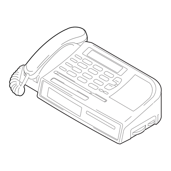
ID TELEPHONE CLOCK RADIO
US Model
Advertisement
Table of Contents

Related Manuals for Sony SCT-ID10


Summary of Contents for Sony SCT-ID10
- Page 1 For power backup : 9V DC, one 6F22 battery (Functions for clock radio only) Battery life : Approx. 35 hours using the Sony S-006P (U) battery Dimensions : Approx. 250 x 98.6 x 202 mm (w/h/d) x 4 x 8 inches) incl. projecting parts and controls Mass Approx.
-
Page 2: Table Of Contents
DIAGRAMMES SCHÉMATIQUES ET LA LISTE DES PIÈCES SONT frequency mark CRITIQUES POUR LA SÉCURITÉ DE FONCTIONNEMENT. NE 10.70MHz REMPLACER CES COMPOSANTS QUE PAR DES PIÈCES SONY blue 10.67MHz DONT LES NUMÉROS SONT DONNÉS DANS CE MANUEL OU DANS LES SUPPLÉMENTS PUBLIÉS PAR SONY. -
Page 3: General
SECTION 1 This section is extracted from GENERAL instruction manual. LOCATION AND FUNCTION OF CONTROLS TONE OPER – 3 –... - Page 4 – 4 –...
- Page 5 – 5 –...
- Page 6 – 6 –...
-
Page 7: Disassembly
SECTION 2 DISASSEMBLY Note : Follow the disassembly procedure in the numerical order given. 2-1. KEY BOARD, CABINET (UPPER) ASSY REMOVAL Cabinet (Upper) assy Rubber key switch CN101 (15 pin) Key board CN102 (7 pin) 5 Screws Cabinet (Lower) assy (+P 2.6x8) 5 Screws (+P 2.6x8) 1 Screws (+P 3x14) -
Page 8: Cabinet (Top) Removal
2-3. CABINET (TOP) REMOVAL 1 Screw (+BTP 3x10) Cabinet (top) Cabinet (bottom) assy INSTALLATION POWER CORD Power cord Cabinet (Lower) Battery blind board Power transformer board – 8 –... -
Page 9: Dial Pointer Installation
SECTION 3 DIAL POINTER INSTALLATION Note : Follow the installation procedure in the numerical order given. Knob (tuning) Marking (A) Pointer 6 Turn the knob (VOL) to the Knob (Vol) arrow direction fully Marking Making portion of the knob (VOL) within arrow A marked area, then attach it... -
Page 10: Test Mode
SECTION 4 TEST MODE 1. Key Input Test (1) Press the [PR OG] , [ERASE] , [*] , [0], [#] buttons simultaneously. (2) A beep tone sounds and test mode is now set. (3) Press the [1] button to set the test mode to key input. (4) A beep tone sounds each time the [CALL W AITIN/FLASH] , [SPEED] , [REDIAL/P AUSE] ……... -
Page 11: Electrical Adjustments
SECTION 5 ELECTRICAL ADJUSTMENTS • Repeat the procedures in each adjustment several times, and the TUNER SECTION frequency coverage and tracking adjustments should be finally • RADIO switch : ON done by the trimmer capacitors. • VOLUME : MIN AM IF ALIGNMENT AM Section Adjust for a maximum reading on level meter. -
Page 12: Diagrams
SECTION 6 DIAGRAMS 6-1. EXPLANATION OF IC TERMINALS IC602 TMP47C853F (SYSTEM CONTROL) Pin No. Pin name Description Data enable output terminal. Read/write select signal output. 0 : Write, 1 : Read Register select signal output. HOOK Hook switch DET. Key return input. Key return input. -
Page 13: Block Diagram
SCT-ID10 6-2. BLOCK DIAGRAM • Signal path. : FM : RX (From Tel Line) : TX (To Tel Line) : bell – 13 – – 14 –... -
Page 14: Schematic Diagram (Main Section)
SCT-ID10 Refer to page 23 for IC Block Diagrams. 6-4. SCHEMATIC DIAGRAM (MAIN SECTION) Note: • All capacitors are in µF unless otherwise noted. pF: µµF • U : B+ Line. • Signal path. WAVEFORM • H : adjustment for repair. -
Page 15: Schematic Diagram (Key Section)
6-6. SCHEMATIC DIAGRAM (KEY SECTION) Refer to page 23 for IC Block Diagrams. SCT-ID10 WAVEFORM Note: • All capacitors are in µF unless otherwise noted. pF: µµF • Voltages are taken with a VOM (Input impedance 10 MΩ). Voltage variations may be noted due to normal produc- 50 WV or less are not indicated except for electrolytics tion tolerances. -
Page 16: Ic Block Diagrams
IC BLOCK DIAGRAMS IC101 BA6566 MUTE INTERFACE DTMF POWER LINE LINE CONTROL DISSIPATION CURRENT SENSE VREG IC201 BA8206 IC301 MT88E43ASR ALERT SIGNAL ANTI-ALIAS – HIGH TONE IN– FILTER FILTER TONE GUARD POWER ST/GT DETECTION TIME SUPPLY ALGORITHM WITH ALERT SIGNAL HYSTERISIS INTERNAL LOW TONE... -
Page 17: Exploded Views
SECTION 7 EXPLODED VIEWS NOTE : • -XX, -X mean standardized parts, so they • The mechanical parts with no reference The components identified by mark ! may have some difference from the original number in the exploded views are not or dotted line with mark ! are critical one. - Page 18 7-2. HAMDSET SECTION MIC1 Ref. No. Part No. Description Remark Ref. No. Part No. Description Remark 3-021-136-01 HAND SET (LOWER) 1-770-505-11 JACK,MODULAR 3-021-135-01 HAND SET (UPPER) MIC1 1-542-161-11 MICROPHONE, ELECTRET CONDENSER * 53 3-021-137-01 WEIGHT 1-550-648-11 RECEIVER, DYNAMIC 3-380-401-01 SPACER (SPEAKER) * 55 1-669-396-11 MICROPHONE RETAINER BOARD –...
-
Page 19: Electrical Parts List
SECTION 8 ELECTRICAL PARTS LIST NOTE : • Due to standardization, replacements in the • SEMICONDUCTORS In each case, u : µ , for example : The components identified by mark ! parts list may be different from the parts uA.. - Page 20 MAIN Ref. No. Part No. Description Remark Ref. No. Part No. Description Remark A-3679-978-A MAIN BOARD, COMPLETE C108 1-163-005-11 CERAMIC CHIP 470PF C109 1-163-005-11 CERAMIC CHIP 470PF ******************** C110 1-163-038-11 CERAMIC CHIP 0.1uF 1-535-804-21 SNAP, BATTERY C111 1-163-012-00 CERAMIC CHIP 0.0018uF 10% 1-769-339-22 CORD, POWER C112...
- Page 21 MAIN Ref. No. Part No. Description Remark Ref. No. Part No. Description Remark 1-151-673-11 CAP, VARIABLE (TUNING) < JUMPER RESISTOR > 1-151-673-11 CAP, VARIABLE (TUNING) 1-151-673-11 CAP, VARIABLE (TUNING) JC401 1-216-295-00 METAL CHIP 1/10W JC402 1-216-295-00 METAL CHIP 1/10W < VARIABLE CAPACITOR > JC403 1-216-295-00 METAL CHIP 1/10W...
- Page 22 MAIN TRANSFORMER TRANSFORMER RETAINER Ref. No. Part No. Description Remark Ref. No. Part No. Description Remark R112 1-247-733-11 CARBON 1/2W F R404 1-249-441-11 CARBON 100K 1/4W R113 1-216-077-00 METAL CHIP 1/10W R405 1-247-903-00 CARBON 1/4W R406 1-247-903-00 CARBON 1/4W R114 1-216-053-00 METAL CHIP 1.5K 1/10W...
- Page 23 SCT-ID10 Ref. No. Part No. Description Remark BZ201 1-505-978-11 PIEZOELECTRIC BUZZER 1-810-027-11 DIODE SL-2994-54TB (DATE DISPLAY) J102 1-770-504-11 JACK, MODULAR (TO HANDSET) LCD601 1-803-112-11 DISPLAY PANEL, LIQUID CRYSTAL MIC1 1-542-161-11 MICROPHONE, ELECTRET CONDENSER 1-504-748-21 SPEAKER (6.6cm) 1-550-648-11 RECEIVER, DYNAMIC ! T2...
Need help?
Do you have a question about the SCT-ID10 and is the answer not in the manual?
Questions and answers