Table of Contents
Advertisement
SERVICE MANUAL
Ver 1.1 1999.07
Dolby noise reduction manufactured under license from
Dolby Laboratories Licensing Corporation.
"DOLBY" and the double-D symbol a are trademarks of
Dolby Laboratories Licensing Corporation.
MICROFILM
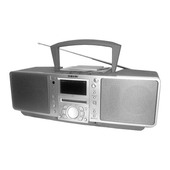
ZS-M50
Model Name Using Similar Mechanism
MD
MD Mechanism Type
Section
Optical Pick-up Type
Model Name Using Similar Mechanism
CD
CD Mechanism Type
Section
Optical Pick-up Type
SPECIFICATIONS
PERSONAL MINIDISC SYSTEM
AEP Model
UK Model
Tourist Model
NEW
MDM-3Z
KMS-260A
CFD-S27
KSM-213CDM
KSS-213C
– Continued on page 2 –
Advertisement
Table of Contents

Related Manuals for Sony ZS-M50


Summary of Contents for Sony ZS-M50
- Page 1 ZS-M50 SERVICE MANUAL AEP Model UK Model Ver 1.1 1999.07 Tourist Model Dolby noise reduction manufactured under license from Model Name Using Similar Mechanism Dolby Laboratories Licensing Corporation. MD Mechanism Type MDM-3Z “DOLBY” and the double-D symbol a are trademarks of Section Dolby Laboratories Licensing Corporation.
-
Page 2: Table Of Contents
TABLE OF CONTENTS 5. ADJUSTMENTS Specifications ................1 MD Section ..............21 1. SERVICE NOTE ............3 CD Section ............... 24 Display Section ..............25 Tuner Section ..............26 2. GENERAL ..............5 6. DIAGRAMS 3. DISASSEMBLY 6-1. Explanation of IC Terminals ........28 3-1. -
Page 3: Service Note
30 cm away from the objective lens. MARK !ON THE SCHEMATIC DIAGRAMS AND IN THE PARTS LIST ARE CRITICAL TO SAFE OPERATION. REPLACE THESE COMPONENTS WITH SONY PARTS WHOSE PART NUMBERS APPEAR AS SHOWN IN THIS MANUAL OR IN LASER DIODE AND FOCUS SEARCH OPERATION SUPPLEMENTS PUBLISHED BY SONY. - Page 4 ABOUT THE BD BOARD WAVEFORM CHECKING JIG The special jig (J-2501-124-A) is highly convenient when check- ing the waveform of the BD board of the MD section. Pin names and items to check are as follows: I+3V : for IOP measurement (check for depleted optical pickup laser) IOP : for IOP measurement (check for depleted optical pickup laser)
-
Page 5: General
SECTION 2 GENERAL LOCATION AND FUNCTION OF CONTROLS FRONT PANEL: MD/CD/RADIO Section 1 MD operation buttons !º YES, ENTER button fl (play/pause) !¡ Jog dial π (stop) =/+ AMS 2 BAND button PRESET 3 CD operation buttons !™ NO, CANCEL button fl... - Page 6 REAR PANEL Section #¢ MW/LW ANTENNA terminal #∞ FM EXT ANTENNA terminal #§ FM rod antenna #¶ ⁄ AC IN jack #• Battery compartment (for memory back-up) #ª RESET button (bottom) $º FM ANTENNA SELECTOR switch REMOTE CONTROL Section 1 TA SERCH button 2 CD OPEN/CLOSE button 3 Numeric buttons OPERATE...
-
Page 7: Disassembly
SECTION 3 DISASSEMBLY The equipment can be removed using the following procedure. < MAIN BLOCK SECTION > Cabinet (Front) Control (L) board sub ASSY Control (R) board Control (F) board, JOG board BATT board Power board Cabinet (Rear) Tuner board, Anetenna SW board Optical pick-up ASSY, CD motor board sub ASSY Cabinet (Upper) -
Page 8: Control (L) Board
3-2. CONTROL (L) BOARD Control (L) board 1 Screws (+B 2.6x8) Cabinet (Front) sub ASSY 3-3. CONTROL (R) BOARD 1 Screws (+B 2.6x8) Control (R) board Cabinet (Front) sub ASSY 3-4. CONTROL (F) BOARD, JOG BOARD 1 Screws (+B 2.6x8) Plate (JOG) , retainer Control (F) board Cabinet (Front) sub ASSY... -
Page 9: Batt Board
3-5. BATT BOARD Cabinet (Rear) sub ASSY Chassis, Transformer 1 Screws (+BV 3x10) BATT board 3-6. POWER BOARD Cabinet (Rear) sub ASSY 1 Screws (+BV 3x20) Power transformer Power board 4 Screws (+BV 4x12) 2 Screws (+BV 3x10) Chassis, Transformer 3-7. -
Page 10: Center Block Section
3-8. CENTER BLOCK SECTION 1 Screws (+BV 3x14) Center Block Section Cabinet (Rear) sub ASSY 2 Screws (+BV 3x12) 3-9. CABINET (UPPER), CHASSIS (MAIN) Cabinet (Upper) 3 Claws 1 Wire , parallel (8 core) 2 Wire , parallel (16 core) (Control sw board : CN550) (CD optical pick-up) 3 Claw... -
Page 11: Optical Pick-Up Assy, Cd Motor Board
3-10. OPTICAL PICK-UP ASSY, CD MOTOR BOARD Cabinet (Upper) CD Optical pick-up ASSY 1 Screws (+PWH 2.6x8) 1 Screws (+PWH 2.6x8) CD Motor board 3 Remove solder 3-11. CONTROL SW BOARD 3-12. MOTOR BOARD, BELT, MOTOR (M703) Cabinet (Upper) Cabinet (Upper) Motor (M703) (Door open/close) Chassis, Motor... -
Page 12: Lcd Board, Bl Board
3-13. LCD BOARD, BL BOARD 4 Screws (+B 2.6x4) 6 Screw (+BV 3x10) 3 LCD Flexible board LCD board Chassis (Main) BL board Holder LCD 1 Screws (+B 2.6x8) 3-14. AUDIO BOARD 1 Screws (+BV 3x10) Audio board Chassis (Main) –... -
Page 13: Line Board
3-15. LINE BOARD Chassis (Main) 3 Screw (+BVTT 2.6x6) Bracket (Line) Main board Line board Bottom Plate 1 Screws (+BV 3x10) 3-16. MAIN BOARD 2 Screw (+BVTT 2.6x6) 1 Screws (+PTPWH 2.6x5) 1 Screw (+BVTT 2.6x6) Bracket (HP) Main board Bottom Plate –... -
Page 14: Md Block Assy
3-17. MD BLOCK ASSY Chassis (Main) MD Block ASSY 1 Screws (+BVTP 2.6x8) 2 Screws (+BVTP 2.6x8) 1 Screws (+BVTP 2.6x8) 2 Screws (+BVTP 2.6x8) <MD BLOCK ASSY SECTION> 3-18. DG BOARD MD Block ASSY 3 Wire , parallel (26 core) DG board 3 Wire , parallel (29 core) 4 Screws (+BVTP 2.6x8) -
Page 15: Chassis (Md)
3-19. CHASSIS (MD) 3 Screws (+BVTP 2.6x8) 3 Screws (+BVTP 2.6x8) Case (Upper) , MD shield 3 Screws (+BVTP 2.6x8) 5 Screws (+BVTT 2x3) Chassis (MD) 5 Screw (+BVTT 2x3) Case (Lower) , MD shield MD Mechanism Block 1 Screws (+BVTP 2.6x8) 1 Screws (+BVTP 2.6x8) 3-20. -
Page 16: Sub Chassis Assy, Md Mechanism Deck
3-21. SUB CHASSIS ASSY, MD MECHANISM DECK 1 Step screws 1 Step screws Insulators Insulators MD mechanism deck When mounting, make sure that A sets in the correct position. SUB Chassis ASSY 3-22. SHUTTER ASSY 1 Washer Sub chassis ASSY 2 Shaft (shutter) Shutter ASSY 3 Shutter ASSY... -
Page 17: Sw Board
3-23. SW BOARD SW board 1 Claws 1 Claws 1 Claws MD mechanism deck 3-24. “ HEAD, OVER WRITE ”, SLIDER ASSY 2 Screw (M1.7x6) Head, Over write 1 Screw (M1.7x2) 6 Position the gear shaft 7 Claw (L) as ahown in the diagram Retainer Slider ASSY 7 Claw... -
Page 18: Md Optical Pick-Up Block
CAUTION DURING SLIDER ASSY ASSEMBLY Slider ASSY Mount the A of the lever (head up) so that it passes above the slider ASSY. Take caution as to not damage the detection switch MD mechanism deck 3-25. MD OPTICAL PICK-UP BLOCK MD Optical pick-up block Shaft (Main shaft) MD mechanism deck... -
Page 19: Test Mode
SECTION 4 TEST MODE 4-1. CAUTIONS WHEN USING THE TEST MODE 4-5. SELECTING THE TEST MODE 1 Check to make sure the inserted disk is completed stopped be- There are 9 types of test modes (see table below). Turning the AMS fore removing since loading related operations will operate re- dial clockwise switches modes shown in the table in the order from gardless of the Test mode operation. -
Page 20: Functions Of Other Buttons
4-5-2. Operating in the Continuous Recording mode 4-7. TEST MODE DISPLAY 1. Entering the Continuous Recording mode The display will switch in the following sequence every time the 1 Insert a disk that may be recorded into the unit (see Note 3) DISPLAY button is pressed. -
Page 21: Adjustments
SECTION 5 ADJUSTMENTS MD SECTION 5-4. CREATING A CONTINUOUS RECORDING DISK 5-1. CAUTION WHEN CHECKING LASER DIODE • This disk is used during focus bias adjustment and error rate EMISSION check. The procedure for creating a continuous recording disk is as follows. Never look from directly above when checking the laser diode emis- sion during adjustment as failure to do so may result in loss of eye- 1. - Page 22 5-6. LASER POWER ADJUSTMENT Specified values: Laser power meter reading : 6.9–7.1mW Connections: Digital voltmeter reading : ±10% the value on the label of the opti- Laser power meter cal pickup. (Optical pick-up label) 260A 27X40 Optical pick-up B0825 objective lens Digital voltmeter In this case, Iop = 82.5mA Iop(mA) = digital voltmeter reading (mV)/1(Ω)
- Page 23 7. Press the YES/ENTER button to save the adjustment result to 18. Press the MD EJECT button to remove the check disk (MD) the non-volatile storage memory (at this time “ EFB= SAVE TDYS-1. ” will be displayed for an instant, then “ EFB= MO-W ”...
-
Page 24: Cd Section
CD SECTION C1 error 1. Enter the CD Test mode (see page 19) 88 07 00 3A0 Focus bias volume (F, BIAS) The above is the default display. Pressing the ^ button will rotate the CD and pressing the YES/ ENTER button once more will output sounds. -
Page 25: Display Section
3. Traverse signal check DISPLAY SECTION DIMMER ADJUSTMENT Connection Point: 1. Connect the LCD1 to the CN533 of the LCD board. 2. Connect the digital voltmeter to the CN533 8 pin of the LCD [MAIN BOARD] (SIDE A) board. 3. Adjust the RV550 of the LCD board for 2.83V reading on digi- tal voltmeter. -
Page 26: Tuner Section
TUNER SECTION 0dB=1µV LW FREQUENCY COVERAGE ADJUSTMENT reading on digital Adjust part Frequency display AM Section voltmeter Function switch : MW or LW Confirmation 153kHz Standard value : 0.5 – 0.9V Volume : MIN Adjustment value :5.5V 297kHz 60cm Standard value : 5.1 – 5.9V loop antenna B loop antenna A LW TRACKING ADJUSTMENT... - Page 27 Connect and Adjustment Location : CFT1 : MW/LW IF Adjustment [TUNER BOARD] (SIDE B) MW/LW frequency coverage FM frequency coverage Digital voltmeter 100 k Ω TP (VT) (VT) – Be sure not to move L9 L3 : LW Tracking Adjustment L4 : MW Tracking Adjustment CT2 : MW Tracking Adjustment CT1 : LW Tracking Adjustment...
-
Page 28: Diagrams
SECTION 6 DIAGRAMS 6-1. EXPLANATION OF IC TERMINALS BD BOARD IC101 MD SECTION RF AMPLIFIER (CXA2523R) Pin No. Pin name Description Input of RF signal l converted from I to V Input of RF signal J converted from I to V. Midpoint voltage (+1.5V) generation output. - Page 29 MAIN BOARD (2/2) IC405 SYSTEM CONTROL (CXP740096-026Q) Pin No. Pin name Description MD function output. RADIO/LINE Radio/LINE function output. ACCHK AC power supply detection input. L : Supplied H : Not supplied – Not used (OPEN). – Not used (OPEN). –...
- Page 30 Pin No. Pin name Description SELECT Destination select detection input. AVSS – A/D converter ground terminal. AVREF – A/D converter reference voltage input. AVDD – A/D converter power supply terminal. LED - PRESET/AMS AMS/PRESET LED drive output. LED - SELECT SELECT LED drive output.
- Page 31 • BD BOARD IC121 digital signal processor, digital servo signal processor, EFM/ACIRC encoder/decoder, shock- proof memory controller, ATRAC encoder/decoder, 2Mbit DRAM (CXD2652AR) DG BOARD IC601 SYSYTEM CONTROL (RU8X12MF-0021) Pin No. Pin name Description Pin No. Pin name Description Pin No. Pin name Description Pin No.
-
Page 32: Block Diagram (Main Section)
ZS-M50 6-2. BLOCK DIAGRAM (MAIN SECTION) • Signal path. : FM : MW/LW : MD PLAY : MD REC : CD – 35 – – 36 – – 37 – – 38 –... -
Page 33: Block Diagram (Md Section)
ZS-M50 6-3. BLOCK DIAGRAM (MD SECTION) Circuit Boards Location CD MOTOR board POWER board AUDIO board MOTOR board CONTROL (L) board ANTENNA SW board JOG board MAIN board CONTROL (F) board CONTROL (R) board LINE board CONTROL SW board BATT board... - Page 35 6-5. SCHEMATIC DIAGRAM – MAIN SECTION (1/3) – Refer to page 89 for IC Block Diagrams. ZS-M50 Waveforms – Main Section (1/3) – PLAY MODE 3.2 Vp-p 1.0 – 1.5 Vp-p 8.7 µ sec IC701 #¡ (RFO) IC702 @ª (PCO) VOLT/DIV : 0.2 V AC...
- Page 36 ZS-M50 6-6. SCHEMATIC DIAGRAM – MAIN SECTION (2/3) – Refer to page 89 for IC Block Diagrams. Waveforms – Main Section (2/3) – 0.5 Vp-p 8 MHz IC405 $™ XTAL VOLT/DIV : 0.1 V AC TIME/DIV : 50 nsec 3.0 Vp-p 32 kHz IC405 *¶...
-
Page 37: Schematic Diagram -Main Section (1/3)
6-7. SCHEMATIC DIAGRAM – MAIN SECTION (3/3) – Refer to page 89 for IC Block Diagrams. ZS-M50 Note: • All capacitors are in µF unless otherwise noted. pF: µµF 50 WV or less are not indicated except for electrolytics and tantalums. -
Page 39: Schematic Diagram -Audio Section
6-9. SCHEMATIC DIAGRAM – AUDIO SECTION – Refer to page 93 for IC Block Diagram. ZS-M50 Note: • All capacitors are in µF unless otherwise noted. pF: µµF 50 WV or less are not indicated except for electrolytics and tantalums. -
Page 40: Schematic Diagram -Dg Section
ZS-M50 6-10. SCHEMATIC DIAGRAM – DG SECTION – Refer to page 93 for IC Block Diagram. Waveforms – DG Section – 0.63 Vp-p 12 MHz IC601 @¶ XOUT VOLT/DIV : 0.2 V AC TIME/DIV : 20 nsec 0.4 Vp-p 32.768 kHz IC601 @¢... -
Page 42: Printed Wiring Boards -Tuner Section
ZS-M50 6-12. PRINTED WIRING BOARDS – TUNER SECTION – Refer to page 42 for Circuit Boards Location. [ANTENNA SW BOARD] ANT1 TELESCOPIC ANTENNA FM ANTENNA SELECTOR 1-675-236- (21) Semiconductor Location [TUNER BOARD] (SIDE B) [TUNER BOARD] (SIDE A) Ref. No. -
Page 43: Schematic Diagram -Tuner Section
ZS-M50 6-13. SCHEMATIC DIAGRAM – TUNER SECTION – Refer to page 94 for IC Block Diagrams. Waveform – Tuner Section – 1.5 Vp-p 75 kHz IC2 @º XOUT VOLT/DIV : 0.5 V AC TIME/DIV : 5 µsec Note: • All capacitors are in µF unless otherwise noted. pF: µµF 50 WV or less are not indicated except for electrolytics and tantalums. -
Page 44: Schematic Diagram -Control Section
6-14. SCHEMATIC DIAGRAM – CONTROL SECTION – ZS-M50 Note: • All capacitors are in µF unless otherwise noted. pF: µµF 50 WV or less are not indicated except for electrolytics and tantalums. • All resistors are in Ω and W or less unless otherwise specified. - Page 47 6-17. SCHEMATIC DIAGRAM – BD SECTION – Refer to page 91 for IC Block Diagram. ZS-M50 Semiconductor Location Waveforms – BD Section – Ref. No. Location D101 PLAY MODE D181 D183 3.3 Vp-p 0.46 Vp-p IC101 E-13 IC103 B-13 IC121 D-11 23.05 µ...
- Page 48 IC Block Diagrams – Main Section – IC702 CXD3009Q IC Block Diagrams – BD Section – IC121 CXD2652AR IC701 CXA2542AQ IC101 CXD2523R 100 99 98 97 96 95 94 93 92 91 90 89 88 87 86 85 84 83 82 81 80 79 78 77 76 59 58 57 56 55 54 46 45 44...
- Page 49 IC Block Diagram – Audio Section – IC312 BH3863F-E2 19 18 17 16 15 14 DINAMIC DIGITAL DINAMIC FILTER FILTER BASS CONTROL BASS TREBLE TREBLE 0dB/6dB 0dB/6dB BASS BASS 10 11 12 IC Block Diagram – DG Section – IC603 PCM3003E/T2 MODE CONTROL INTERFACE ANALOG...
- Page 50 IC Block Diagrams – Tuner Section – IC1 TA2008AN FM MPX BUFF BUFF BUFF BUFF AM/FM ST/MONO 1/8DIV LEVEL MUTE IC2 LC72137M-TLM 16 15 14 FILTER POWER RESET PHASE DETECTOR REFERENCE CHARGE PUMP DIVIDER UNLOCK DETECTOR SWALLOW COUNTER 1/16. 1/17 4 BITS 12 BIT PROGRAMBLE DIVIDER DATA SHIFT REGISTER...
-
Page 51: Exploded Views
SECTION 7 EXPLODED VIEWS NOTE : • -XX, -X mean standardized parts, so they • The mechanical parts with no reference The components identified by mark ! may have some difference from the original number in the exploded views are not or dotted line with mark ! are critical one. -
Page 52: Front Cabinet Section
7-2. FRONT CABINET SECTION 4 A : Control (R) board 4 B : Control (F) board 4 C : JOG board 4 D : Control (L) board SP301 SP302 (including 4 A– 4 D) Ref. No. Part No. Description Remark Ref. -
Page 53: Center Block Section
7-3. CENTER BLOCK SECTION not supplied LCD1 Ref. No. Part No. Description Remark Ref. No. Part No. Description Remark * 101 1-671-318-21 LINE BOARD 1-783-958-11 WIRE, PARALLEL (FFC) (11 CORE) 4-931-757-31 SCREW(DIA.2.6X8)(IT3B),TAPPING 1-783-957-11 WIRE, PARALLEL (FFC) (8 CORE) * 103 3-378-400-01 CUSHION, SARANET * 104 3-027-672-01 HOLDER, LCD... -
Page 54: Upper Cabinet Section
7-4. UPPER CABINET SECTION supplied M703 supplied Ref. No. Part No. Description Remark Ref. No. Part No. Description Remark 1-783-955-11 WIRE, PARALLEL (FFC) (16 CORE) 3-028-820-01 LEVER (O/C) * 152 1-639-678-12 CD MOTOR BOARD 3-027-667-01 GEAR (C) 3-921-725-01 SCREW (2.6X10), +PWH 3-027-668-01 GEAR (D) 3-931-379-01 RUBBER, VIBRATION PROOF (RED) 3-017-031-21 GEAR (A) -
Page 55: Md Section (1)
7-5. MD SECTION (1) (MDM-3Z) not supplied not supplied not supplied not supplied Ref. No. Part No. Description Remark Ref. No. Part No. Description Remark 4-931-757-31 SCREW(DIA.2.6X8)(IT3B),TAPPING X-3377-791-1 SHUTTER ASSY * 202 A-3323-164-A DG BOARD, COMPLETE 1-783-961-11 WIRE, PARALLEL (FFC) (19 CORE) 1-660-966-11 OP RALAY FLEXIBLE BOARD * 204 3-027-682-01 CHASSIS (MD) -
Page 56: Md Section (2)
7-6. MD SECTION (2) (MDM-3Z) not supplied supplied not supplied M903 M902 HR901 M901 not supplied The components identified by mark ! or dotted line with mark ! are critical for safety. Replace only with part number specified. Ref. No. Part No. -
Page 57: Cd Optical Pick-Up Section
7-7. CD OPTICAL PICK-UP SECTION (KSM-213CDM) not supplied (including M702) M702 M701 The components identified by mark ! or dotted line with mark ! are critical for safety. Replace only with part number specified. Ref. No. Part No. Description Remark Ref. -
Page 58: Electrical Parts List
SECTION 8 ANTENNA SW AUDIO ELECTRICAL PARTS LIST NOTE : • Due to standardization, replacements in the • SEMICONDUCTORS In each case, u : µ , for example : The components identified by mark ! parts list may be different from the parts uA.. - Page 59 AUDIO Ref. No. Part No. Description Remark Ref. No. Part No. Description Remark C338 1-104-665-11 ELECT 100uF < RESISTOR > C339 1-163-021-91 CERAMIC CHIP 0.01uF R101 1-216-013-00 METAL CHIP 1/10W C341 1-107-682-11 CERAMIC CHIP R111 1-216-295-00 METAL CHIP 1/10W C342 1-107-725-11 CERAMIC CHIP 0.1uF R112...
- Page 60 AUDIO BATT Ref. No. Part No. Description Remark Ref. No. Part No. Description Remark R319 1-216-049-91 RES,CHIP 1/10W C132 1-107-823-11 CERAMIC CHIP 0.47uF R320 1-216-121-91 RES,CHIP 1/10W C133 1-163-017-00 CERAMIC CHIP 0.0047uF 5% R321 1-216-041-00 METAL CHIP 1/10W C134 1-163-038-91 CERAMIC CHIP 0.1uF R322 1-216-025-91 RES,CHIP...
- Page 61 Ref. No. Part No. Description Remark Ref. No. Part No. Description Remark IC152 8-759-430-25 IC BH6511FS R140 1-216-029-00 METAL CHIP 1/10W IC171 8-759-428-58 IC XL24C01AF-E2 R141 1-216-295-00 METAL CHIP 1/10W IC181 8-759-095-65 IC TC74ACT540FS R142 1-216-073-00 METAL CHIP 1/10W IC192 8-759-426-95 IC L88MS33T-TL R143 1-216-073-00 METAL CHIP...
- Page 62 CD MOROR CONTROL (F) CONTROL (L) CONTROL (R) Ref. No. Part No. Description Remark Ref. No. Part No. Description Remark 1-639-678-12 CD MOTOR BOARD < IC > **************** IC550 8-742-129-00 HYB SBX1971-51P < CONNECTOR > < RESISTOR > CNP707 1-564-722-11 PIN, CONNECTOR (SMALL TYPE) 6P R570 1-216-045-00 METAL CHIP 1/10W...
- Page 63 CONTROL SW Ref. No. Part No. Description Remark Ref. No. Part No. Description Remark A-3321-849-A CONTROL SW BOARD C611 1-164-156-11 CERAMIC CHIP 0.1uF C612 1-164-156-11 CERAMIC CHIP 0.1uF ****************** C613 1-162-927-11 CERAMIC CHIP 100PF < CAPACITOR > C614 1-163-251-11 CERAMIC CHIP 100PF C615 1-164-156-11 CERAMIC CHIP...
- Page 64 Ref. No. Part No. Description Remark Ref. No. Part No. Description Remark D602 8-719-988-61 DIODE 1SS355TE-17 FB658 1-500-445-21 FERRITE < FERRITE BEAD > < FILTER > FB601 1-500-445-21 FERRITE FL601 1-239-901-21 FERRITE FB602 1-469-125-21 FERRITE FL602 1-239-901-21 FERRITE FB603 1-469-125-21 FERRITE FL603 1-239-899-21 FILTER, CHIP EMI FB604...
- Page 65 Ref. No. Part No. Description Remark Ref. No. Part No. Description Remark L610 1-414-398-11 INDUCTOR 10uH R626 1-216-073-00 METAL CHIP 1/10W R627 1-216-841-11 METAL CHIP 1/16W L611 1-416-107-21 INDUCTOR R628 1-216-089-91 RES,CHIP 1/10W L612 1-414-398-11 INDUCTOR 10uH R629 1-216-833-91 RES,CHIP 1/16W L613 1-414-398-11 INDUCTOR...
- Page 66 LINE MAIN Ref. No. Part No. Description Remark Ref. No. Part No. Description Remark < CAPACITOR > A-3323-157-A MAIN BOARD, COMPLETE ********************* C559 1-163-009-11 CERAMIC CHIP 0.001uF C560 1-163-009-11 CERAMIC CHIP 0.001uF 7-685-646-79 SCREW +BVTP TYPE2 N-S C561 1-163-251-11 CERAMIC CHIP 100PF C562 1-163-251-11 CERAMIC CHIP...
- Page 67 MAIN Ref. No. Part No. Description Remark Ref. No. Part No. Description Remark C412 1-126-925-11 ELECT 470uF C471 1-162-927-11 CERAMIC CHIP 100PF C413 1-162-970-11 CERAMIC CHIP 0.01uF C472 1-162-927-11 CERAMIC CHIP 100PF C414 1-124-589-11 ELECT 47uF C473 1-162-927-11 CERAMIC CHIP 100PF C475 1-162-964-11 CERAMIC CHIP...
- Page 68 MAIN Ref. No. Part No. Description Remark Ref. No. Part No. Description Remark C710 1-107-826-91 CERAMIC CHIP 0.1uF C776 1-127-688-21 TANTAL. CHIP 10uF 6.3V C711 1-107-826-91 CERAMIC CHIP 0.1uF C777 1-126-382-11 ELECT 100uF C778 1-162-970-11 CERAMIC CHIP 0.01uF C712 1-115-467-11 CERAMIC CHIP 0.22uF C779 1-162-927-11 CERAMIC CHIP...
- Page 69 MAIN Ref. No. Part No. Description Remark Ref. No. Part No. Description Remark FB413 1-469-185-11 FERRITE L701 1-412-973-11 INDUCTOR 0.33uH FB414 1-500-445-21 FERRITE FB415 1-500-445-21 FERRITE < TRANSISTOR > FB416 1-216-295-00 METAL CHIP 1/10W FB417 1-469-125-21 FERRITE Q101 8-729-920-31 TRANSISTOR DTC343TK Q102 8-729-920-31 TRANSISTOR DTC343TK FB418...
- Page 70 MAIN Ref. No. Part No. Description Remark Ref. No. Part No. Description Remark R117 1-216-073-00 METAL CHIP 1/10W R329 1-216-097-91 RES,CHIP 100K 1/10W R118 1-216-073-00 METAL CHIP 1/10W R119 1-216-821-11 METAL CHIP 1/16W R330 1-216-097-91 RES,CHIP 100K 1/10W R120 1-216-081-00 METAL CHIP 1/10W R331 1-216-833-91 RES,CHIP...
- Page 71 MAIN Ref. No. Part No. Description Remark Ref. No. Part No. Description Remark R452 1-216-833-91 RES,CHIP 1/16W R706 1-216-847-11 METAL CHIP 150K 1/16W R453 1-216-821-11 METAL CHIP 1/16W R454 1-216-817-11 METAL CHIP 1/16W R710 1-218-273-11 RES,CHIP 510K 1/16W R455 1-216-817-11 METAL CHIP 1/16W R711 1-216-847-11 METAL CHIP...
- Page 72 MAIN MOTOR POWER Ref. No. Part No. Description Remark Ref. No. Part No. Description Remark R791 1-216-821-11 METAL CHIP 1/16W < SWITCH > R792 1-216-809-11 METAL CHIP 1/16W R793 1-216-821-11 METAL CHIP 1/16W S761 1-572-126-21 SWITCH, PUSH (1 KEY) (OPEN) R794 1-216-817-11 METAL CHIP 1/16W...
- Page 73 POWER TUNER Ref. No. Part No. Description Remark Ref. No. Part No. Description Remark < TRANSFORMER > 1-162-964-11 CERAMIC CHIP 0.001uF 1-162-964-11 CERAMIC CHIP 0.001uF ! T901 1-433-781-11 TRANSFORMER, POWER 1-164-505-11 CERAMIC CHIP 2.2uF ! T902 1-433-630-11 TRANSFORMER, LINE FILTER (LFT) 1-162-970-11 CERAMIC CHIP 0.01uF **************************************************************...
- Page 74 TUNER Ref. No. Part No. Description Remark Ref. No. Part No. Description Remark < FERRITE BEAD > 1-216-017-91 RES,CHIP 1/10W 1-216-041-00 METAL CHIP 1/10W 1-414-598-11 INDUCTOR CHIP 1-414-598-11 INDUCTOR CHIP 1-216-049-91 RES,CHIP 1/10W 1-414-598-11 INDUCTOR CHIP 1-216-023-00 METAL CHIP 1/10W 1-414-598-11 INDUCTOR CHIP 1-216-829-11 METAL CHIP 4.7K...
- Page 75 Ref. No. Part No. Description Remark Ref. No. Part No. Description Remark 1-783-957-11 WIRE, PARALLEL (FFC) (8 CORE) 7-627-852-28 +P 1.7X3 1-783-956-11 WIRE, PARALLEL (FFC) (9 CORE) 7-685-133-19 SCREW +P 2.6X6 TYPE2 SLIT 7-685-647-79 SCREW +BVTP 3X10 TYPE2 N-S 1-783-960-11 WIRE, PARALLEL (FFC) (26 CORE) * 122 1-562-327-00 SOCKET, CONNECTOR 3P 7-685-850-01 SCREW +BVTT 2X3 (S)
- Page 76 ZS-M50 Sony Corporation 99G02032-1 9-924-996-12 Personal Audio Company Printed in Japan © 1999.7 – 120 – Published by General Engineering Dept.
Need help?
Do you have a question about the ZS-M50 and is the answer not in the manual?
Questions and answers