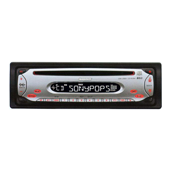
Sony CDX-L480X Service Manual
Fm/mw/lw compact disc player
Hide thumbs
Also See for CDX-L480X:
- Operating instructions manual (116 pages) ,
- Installation/connections (2 pages) ,
- Service manual (40 pages)
Table of Contents
Advertisement
SERVICE MANUAL
Ver 1.0 2002. 12
• The tuner and CD sections have no adjustments.
CD player section
Signal-to-noise ratio
90 dB
Frequency response
10 – 20,000 Hz
Wow and flutter
Below measurable limit
Tuner section
FM
Tuning range
87.5 – 108.0 MHz
Aerial terminal
External aerial connector
Intermediate frequency 10.7 MHz/450 kHz
Usable sensitivity
9 dBf
Selectivity
75 dB at 400 kHz
Signal-to-noise ratio
67 dB (stereo),
69 dB (mono)
Harmonic distortion at 1 kHz
0.5% (stereo),
0.3% (mono)
Separation
35 dB at 1 kHz
Frequency response
30 – 15,000 Hz
MW/LW
Tuning range
MW: 531 – 1,602 kHz
LW: 153 – 279 kHz
Aerial terminal
External aerial connector
Intermediate frequency 10.7 MHz/450 kHz
Sensitivity
MW: 30 µV
LW: 40 µV
Power amplifier section
Outputs
Speaker outputs
(sure seal connectors)
Speaker impedance
4 – 8 ohms
Maximum power output 45 W × 4 (at 4 ohms)
Sony Corporation
9-874-257-01
2002L0400-1
e Vehicle Company
© 2002. 12
Published by Sony Engineering Corporation
CDX-L480X
Model Name Using Similar Mechanism
CD Drive Mechanism Type
Optical Pick-up Name
SPECIFICATIONS
General
Outputs
Inputs
Tone controls
Power requirements
Dimensions
Mounting dimension
Mass
Supplied accessories
Design and specifications are subject to change without
notice.
FM/MW/LW COMPACT DISC PLAYER
AEP Model
UK Model
CDX-L380X
MG-393XA-121//Q
KSS-720A
Audio outputs (rear)
Power aerial relay control
terminal
Telephone ATT control
terminal
Low:
±10 dB at 60 Hz (XPLOD)
Mid:
±10 dB at 1 kHz (XPLOD)
High:
±10 dB at 10 kHz (XPLOD)
12 V DC car battery
(negative earth)
Approx. 178 × 50 × 176 mm
(w/h/d)
Approx. 182 × 53 × 161 mm
(w/h/d)
Approx. 1.2 kg
Parts for installation and
connections
Front panel case (1)
1
Advertisement
Table of Contents

Related Manuals for Sony CDX-L480X


Summary of Contents for Sony CDX-L480X
- Page 1 Speaker outputs (sure seal connectors) Speaker impedance 4 – 8 ohms Maximum power output 45 W × 4 (at 4 ohms) FM/MW/LW COMPACT DISC PLAYER Sony Corporation 9-874-257-01 2002L0400-1 e Vehicle Company © 2002. 12 Published by Sony Engineering Corporation...
- Page 2 COMPONENTS IDENTIFIED BY MARK 0 OR DOTTED LINE WITH MARK 0 ON THE SCHEMATIC DIAGRAMS AND IN THE PARTS LIST ARE CRITICAL TO SAFE OPERATION. REPLACE THESE COMPONENTS WITH SONY PARTS WHOSE PART NUMBERS APPEAR AS SHOWN IN THIS MANUAL OR IN SUPPLEMENTS PUBLISHED BY SONY.
- Page 3 CDX-L480X UNLEADED SOLDER Boards requiring use of unleaded solder are printed with the lead free mark (LF) indicating the solder contains no lead. (Caution: Some printed circuit boards may not come printed with the lead free mark due to their particular size.) : LEAD FREE MARK Unleaded solder has the following characteristics.
-
Page 4: Table Of Contents
CDX-L480X TABLE OF CONTENTS 1. GENERAL Location of controls ..............5 Connections ................6 2. DISASSEMBLY 2-1. Sub Panel Assy ..............7 2-2. CD Mechanism Block ............8 2-3. Main Board ................. 8 2-4. Heat Sink ................9 2-5. Chassis (T.U) Assy .............. 9 2-6. -
Page 5: General
CDX-L480X SECTION 1 GENERAL This section is extracted from instruction manual. -
Page 6: Connections
CDX-L480X Connections... -
Page 7: Disassembly
CDX-L480X SECTION 2 DISASSEMBLY Note : This set can be disassemble according to the following sequence. 2-5. CHASSIS (T.U) ASSY 2-1. SUB PANEL ASSY (Page 9) (Page 7) 2-6. DISC IN BOARD 2-7. SERVO BOARD 2-2. CD MECHANISM BLOCK (Page 10) -
Page 8: Cd Mechanism Block
CDX-L480X 2-2. CD MECHANISM BLOCK 7 bracket (CD) 5 CD mechanism block 6 PTT 2.6x4 2 PTT 2.6x6 1 PTT 2.6x6 4 CNP301 2-3. MAIN BOARD 3 PTT 2.6x6 (ground point) 5 MAIN board 4 PTT 2.6x6 (ground point) 1 PTT 2.6x6... -
Page 9: Heat Sink
CDX-L480X 2-4. HEAT SINK 5 heat sink 3 PTT 2.6x8 2 PTT 2.6x12 1 PTT 2.6x8 2-5. CHASSIS (T.U) ASSY 2 P 2x3 3 P 2x3 1 Unsolder the 4 chassis (T.U) assy lead wires. black white... -
Page 10: Disc In Board
CDX-L480X 2-6. DISC IN BOARD 4 guide (disc) 1 PS 2x3 2 DISC IN board 3 claws 2-7. SERVO BOARD 7 SERVO board 6 PS 2x4 5 PS 2x4 2 Removal the solders. 8 PICK-UP FLEXIBLE board 1 CN3 3 P 2x3... -
Page 11: Shaft Roller Assy
CDX-L480X 2-8. SHAFT ROLLER ASSY • When installing, take note of the positions arm (roller) and washers. (Fig. 1) 3 retaining ring (roller) bearing (roller) bearing (roller) 4 bearing (roller) washer (RA) retaining ring (roller) washer (RA) Fig. 1 5 shaft roller assy... -
Page 12: Optical Pick-Up Block
CDX-L480X 2-10. OPTICAL PICK-UP BLOCK 4 P 2x3 1 P 2x3 5 leaf spring (feed) 2 sled motor assy 3 optical pick-up block 6 shaft (feed) assy... -
Page 13: Diagrams
CDX-L480X SECTION 3 DIAGRAMS 3-1. IC PIN DESCRIPTION • IC501 MN101C49KSG (SYSTEM CONTROL) Pin No. Pin Name Pin Description VREF– — A/D converter power supply (–) pin S-meter voltage detection input QUALITY Noise detection input 4, 5 KEYIN1, 0 Key input 1, 0... - Page 14 CDX-L480X Pin No. Pin Name Pin Description X_EN Not used. (Open) LIMIT CD mechanism deck Limit switch detection input Not used. (Open) D_SW CD mechanism deck Down switch detection input INSW CD mechanism deck Disc in switch detection input Not used. (Open)
-
Page 15: Block Diagram -Tuner Section
CDX-L480X 3-2. BLOCK DIAGRAM — CD SECTION — RF AMP,DIGITAL SERVO, DIGITAL SIGNAL PROCESSOR OPTICAL PICK-UP (KSS-720A) (Page 16) TUNER SECTION LOUT SYSTEM CONTROL ROUT IC501 (1/3) CONV DEMOD PACK CD PACK DSUB CODE TSTB PROCESS TSTB CONV. CD_TSO CD_TSI... -
Page 16: Block Diagram -Cd Section
CDX-L480X 3-3. BLOCK DIAGRAM — TUNER SECTION — SOUND CONTROL ELECTRONIC VOLUME IC401 J330 AUDIO OUT REAR AUDIO 8.3V R-CH BUS-LCH POWER AMP IC750 (1/2) CN601 EFFECT CD-LCH MUTE Q441 TUNER UNIT R-CH (Page 15) SECTION TONE TV-LCH 1 ANT... -
Page 17: Circuit Boards Location
CDX-L480X 3-5. CIRCUIT BOARDS LOCATION 3-4. BLOCK DIAGRAM — DISPLAY SECTION — SERVO board SYSTEM CONTROL LCD DRIVER IC501 (3/3) IC901 KEY MATRIX SUB (CD) board LSW904,905, KEYIN0 DISC IN board LCDSO DATA LSW907-911, LSW913-921 LCDCKO LIMIT board SEG1 S900-903,906,912... -
Page 18: Printed Wiring Boards -Cd Mechanism Section
CDX-L480X 3-6. PRINTED WIRING BOARDS — CD MECHANISM SECTION — • Refer to page 17 for Circuit Boards Location. : Uses unleaded solder. THIS NOTE IS COMMON FOR PRINTED WIRING BOARDS AND SCHEMATIC DIAGRAMS. (In addition to this, the necessary note is printed in each block.) - Page 19 CDX-L480X : Uses unleaded solder. TP77 TP78 TP62 TP82 TP48 TP66 TP80 TP84 TP83 TP60 TP12 TP11 TP50 (Page 21) TP47 C9 C10 TP64 TP10 TP51 TP89 TP59 TP52 TP71 TP56 TP22 TP58 TP72 TP24 TP23 TP25 TP61 TP76 TP88...
-
Page 20: Schematic Diagram -Cd Mechanism Section
CDX-L480X 3-7. SCHEMATIC DIAGRAM — CD MECHANISM SECTION — • Refer to page 17 for Waveforms and page 18 for Common Note on Schematic Diagram. • Refer to page 26 for IC Block Diagrams. TP9 TP8 TP77 TP78 TP89 TP79... -
Page 21: Printed Wiring Board -Main Section
CDX-L480X 3-8. PRINTED WIRING BOARD — MAIN SECTION — • Refer to page 17 for Circuit Boards Location and page 18 for Common Note on Printed Wiring Boards. : Uses unleaded solder. J330 CN601 D752 R452 C765 C764 F901 C751... -
Page 22: Schematic Diagram -Main Section (1/2)
CDX-L480X 3-9. SCHEMATIC DIAGRAM — MAIN SECTION (1/2) — • Refer to page 17 for Waveforms and page 18 for Common Note on Schematic Diagram. • Refer to page 26 for IC Block Diagrams. J330 C332 C333 JC29 C765 C764... -
Page 23: Schematic Diagram -Main Section (2/2)
CDX-L480X 3-10. SCHEMATIC DIAGRAM — MAIN SECTION (2/2) — • Refer to page 18 for Common Note on Schematic Diagram. (Page 22) JC401 L502 R521 R536 R520 R539 (Page 20) R522 R535 C301 C303 R531 R518 JC304 R534 C623 L306... -
Page 24: Printed Wiring Board -Key Section
CDX-L480X 3-11. PRINTED WIRING BOARD — KEY SECTION — • Refer to page 17 for Circuit Boards Location and page 18 for Common Note on Printed Wiring Boards. : Uses unleaded solder. LED903 LED900 LED952 S903 S900 R965 R964 R941... -
Page 25: Schematic Diagram -Key Section
CDX-L480X 3-12. SCHEMATIC DIAGRAM — KEY SECTION — • Refer to page 18 for Common Note on Schematic Diagram. R941 R951 R954 R956 R964 R987 R972 CN901 R942 R944 R952 R955 R957 R961 R965 R988 LED900 LED912 LED902 LED903 R989... -
Page 26: Ic Block Diagrams
CDX-L480X 3-13. IC BLOCK DIAGRAMS IC1 µPD63711GC-8EU IC2 BA5810FP-E2 BIAS 71 70 LOADING PRE OPIN4+ FWD REV – OPIN4– MICROCOMPUTER INTERFACE AGCI 50 C2D3 LDCONT COMPARATOR 49 C2D2 POWER CD-TEXT DECODER OPOUT4 SAVE 48 C2D1 SUB-CODE PROCESSOR OPIN3+ MEMORY 47 C1D2 –... - Page 27 CDX-L480X IC401 BD3803F-FE2 OUT- OUT- OUT- OUT- D-GND MUTE FADER FADER FADER FADER (0~-58, (0~-58, (0~-58, (0~-58, C BUS -∞dB) -∞dB) -∞dB) -∞dB) LOGIC TONE TONE PASS PASS BASS,TREBLE, MIDDLE BASS,TREBLE, MIDDLE (-15dB~+15dB,1dB STEP) (-15dB~+15dB,1dB STEP) VOLUME VOLUME (+23~-79dB,-∞dB (+23~-79dB,-∞dB...
- Page 28 CDX-L480X IC750 TDA8589J/N1 OUT-FL- C BUS OUT-FL+ OUT-RL- PGND3 OUT-RL+ IN-RL IN-FL S-GND PROTECTION/ DIAGNOSTIC IN-FR IN-RR BEEP OUT-RR+ PGND2 OUT-RR- OUT-FR+ STANDBY/ MUTE OUT-FR- CHIP DETECT/ PGND1 DIAGNOSTIC BATTERY TEMPERATURE DIAG DETECTION ENABLE PROTECTION LOGIC SWITCH ANT-REM CRES AMP-REM SWITCH AUDIO8.3V...
-
Page 29: Exploded Views
CDX-L480X SECTION 4 EXPLODED VIEWS NOTE: • The mechanical parts with no reference • Color Indication of Appearance Parts The components identified by mark 0 or dotted line with mark number in the exploded views are not supplied. Example : 0 are critical for safety. -
Page 30: Front Panel Section
CDX-L480X 4-2. FRONT PANEL SECTION LCD901 not supplied not supplied not supplied (KEY board) supplied supplied not supplied supplied supplied Ref. No. Part No. Description Remark Ref. No. Part No. Description Remark X-3382-710-1 PANEL SUB ASSY, FRONT X-3383-264-1 CASE ASSY (for FRONT PANEL) -
Page 31: Cd Mechanism Section (1)
CDX-L480X 4-3. CD MECHANISM SECTION (1) (MG-393XA-121//Q) not supplied supplied not supplied not supplied not supplied M903 Ref. No. Part No. Description Remark Ref. No. Part No. Description Remark A-3315-247-B CHASSIS (T.U) ASSY 3-225-784-01 SPRING (RA3), TENSION 3-931-909-01 SPRING (LR), TENSION... -
Page 32: Cd Mechanism Section (2)
CDX-L480X 4-4. CD MECHANISM SECTION (2) (MG-393XA-121//Q) not supplied Ref. No. Part No. Description Remark Ref. No. Part No. Description Remark X-3378-956-8 ARM ASSY, CHUCKING A-3315-243-D CHASSIS (M) ASSY 3-931-897-61 DAMPER (T) 3-220-180-01 SPRING (TR2), TENSION 3-039-627-01 LEVER (D) 3-931-881-03 LEVER (LOCK) -
Page 33: Cd Mechanism Section (3)
CDX-L480X 4-5. CD MECHANISM SECTION (3) (MG-393XA-121//Q) M901 not supplied (LIMIT board) M902 not supplied (SUB (CD) board) The components identified by mark 0 or dotted line with mark 0 are critical for safety. Replace only with part number specified. -
Page 34: Electrical Parts List
CDX-L480X SECTION 5 DISC IN ELECTRICAL PARTS LIST NOTE: • Due to standardization, replacements in • Items marked “*” are not stocked since The components identified by mark 0 or dotted line with mark the parts list may be different from the they are seldom required for routine service. - Page 35 CDX-L480X MAIN Ref. No. Part No. Description Remark Ref. No. Part No. Description Remark R941 1-216-025-11 RES-CHIP 1/10W 1-162-970-11 CERAMIC CHIP 0.01uF R942 1-216-025-11 RES-CHIP 1/10W 1-124-589-11 ELECT 47uF R943 1-216-021-00 METAL CHIP 1/10W 1-162-915-11 CERAMIC CHIP 10PF 0.5PF R944...
- Page 36 CDX-L480X MAIN Ref. No. Part No. Description Remark Ref. No. Part No. Description Remark C757 1-124-233-11 ELECT 10uF < JUMPER RESISTOR > C758 1-124-233-11 ELECT 10uF C759 1-124-233-11 ELECT 10uF 1-216-296-11 SHORT CHIP C760 1-124-584-00 ELECT 100uF JC21 1-216-296-11 SHORT CHIP...
- Page 37 CDX-L480X MAIN SERVO Ref. No. Part No. Description Remark Ref. No. Part No. Description Remark < RESISTOR > R532 1-216-845-11 METAL CHIP 100K 1/10W R533 1-216-845-11 METAL CHIP 100K 1/10W 1-216-821-11 METAL CHIP 1/10W R534 1-216-833-11 METAL CHIP 1/10W 1-216-809-11 METAL CHIP...
- Page 38 CDX-L480X SERVO Ref. No. Part No. Description Remark Ref. No. Part No. Description Remark 1-125-837-11 CERAMIC CHIP 6.3V 1-216-833-11 METAL CHIP 1/10W 1-162-970-11 CERAMIC CHIP 0.01uF 1-216-833-11 METAL CHIP 1/10W 1-162-970-11 CERAMIC CHIP 0.01uF 1-216-789-11 METAL CHIP 1/10W 1-162-970-11 CERAMIC CHIP 0.01uF...
- Page 39 CDX-L480X Ref. No. Part No. Description Remark PARTS FOR INSTALLATION AND CONNECTIONS *************************************** X-3382-647-1 FRAME ASSY, FITTING X-3382-926-1 SCREW ASSY (BS), FITTING 3-349-410-11 BUSHING 3-246-468-01 COLLAR 1-465-459-21 ADAPTOR, ANTENNA 3-246-471-01 KEY (FRAME) 1-776-527-61 CORD (WITH CONNECTOR) (ISO) (POWER)
- Page 40 CDX-L480X REVISION HISTORY Clicking the version allows you to jump to the revised page. Also, clicking the version at the upper on the revised page allows you to jump to the next revised page. Ver. Date Description of Revision 2002. 12...
Need help?
Do you have a question about the CDX-L480X and is the answer not in the manual?
Questions and answers