Table of Contents
Advertisement
SERVICE MANUAL
Ver. 1.5 2006.05
US and foreign patents licensed from Dolby
Laboratories.
Audio playing system
MiniDisc digital audio system
Laser diode properties
Material: GaAlAs
Wavelength: λ = 790 nm
Emission duration: continuous
Laser output: less than 44.6 µW
(This output is the value measured at a distance
of 200 mm from the lens surface on the optical
pick-up block with 7 mm aperture.)
Recording and playback time (when
using MDW-80)
Maximum 160 min. in monaural
Maximum 320 min. in LP4 stereo
Revolutions
350 rpm to 3,600 rpm (CLV)
Error correction
ACIRC (Advanced Cross Interleave Reed
Solomon Code)
Sampling frequency
44.1 kHz
Sampling rate converter
Input: 32 kHz/44.1 kHz/48 kHz
Coding
ATRAC (Adaptive TRansform Acoustic
Coding)
ATRAC3 — LP2/LP4
Modulation system
EFM (Eight to Fourteen Modulation)
Frequency response
20 to 20,000 Hz ± 3 dB
Sony Corporation
9-877-146-06
2006E16-1
Personal Audio Division
C 2006.05
Published by Sony Techno Create Corporation
SILVER MODEL
Model Name Using Similar Mechanism
Mechanism Type
Optical Pick-up Name
SPECIFICATIONS
Inputs
1)
MIC: stereo mini-jack
(minimum input level 0.25 mV)
Line in: stereo mini-jack for analog input
(minimum input level 49 mV)
optical (digital) mini-jack for optical
(digital) input
Outputs
2)
i/LINE OUT
: stereo mini-jack (dedicated
remote control jack)/194 mV (10 kΩ)
2)
Maximum output (DC)
Headphones:
4 mW + 4 mW (16 Ω)(AEP,UK models)
5 mW + 5 mW (16 Ω)(other models)
Power requirements
Sony AC Power Adaptor connected at the DC
IN 3V jack:
120 V AC, 60 Hz (Models for USA, Canada,
Mexico and Taiwan)
230 - V AC, 50/60 Hz (Models for continental
Europe)
240 V AC, 50 Hz (Model for Australia)
220 V AC, 50 Hz (Model for China)
230 - V AC, 50 Hz (Models for U.K. and
Hong Kong)
100 - 240 V AC, 50/60 Hz (Other models)
The recorder:
Nickel metal hydride rechargeable battery
NH-14WM, 1.2V, 1350mAh (MIN), Ni-MH
LR6 (size AA) alkaline battery
Battery charging stand:
AC power adaptor DC 3V
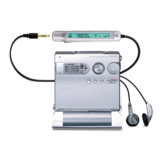
PORTABLE MINIDISC RECORDER
MZ-N910
Australian Model
Chinese Model
Tourist Model
Battery operation time
When recording
(Unit: approx.hours)(JEITA
Batteries
NH-14WM
nickel metal
hydride
rechargeable
battery
LR6 (SG)
Sony alkaline
dry battery
NH-14WM
nickel metal
hydride
rechargeable
battery + One
LR6 (SG)
When playing
Batteries
NH-14WM
nickel metal
hydride
rechargeable
battery
LR6 (SG)
Sony alkaline
dry battery
NH-14WM
nickel metal
hydride
rechargeable
battery + One
LR6 (SG)
– Continued on next page –
AEP Model
UK Model
E Model
NEW
MT-MZN910-181
ABX-1R
3)
4)
)
SP
LP2
LP4
Stereo
Stereo
Stereo
11
16
20
11
16
21
29
38
50
SP
LP2
LP4
Stereo
Stereo
Stereo
31
38
45
47
57
69
80
95
114
Advertisement
Table of Contents

Related Manuals for Sony Walkman MZ-N910


Summary of Contents for Sony Walkman MZ-N910
- Page 1 Revolutions hydride Power requirements rechargeable 350 rpm to 3,600 rpm (CLV) Sony AC Power Adaptor connected at the DC battery + One Error correction IN 3V jack: LR6 (SG) ACIRC (Advanced Cross Interleave Reed 120 V AC, 60 Hz (Models for USA, Canada,...
- Page 2 COMPONENTS IDENTIFIED BY MARK 0 OR DOTTED LINE WITH MARK 0 ON THE SCHEMATIC DIAGRAMS AND IN THE PARTS LIST ARE CRITICAL TO SAFE OPERATION. REPLACE THESE COMPONENTS WITH SONY PARTS WHOSE PART NUMBERS APPEAR AS SHOWN IN THIS MANUAL OR IN SUPPLEMENTS PUBLISHED BY SONY.
-
Page 3: Table Of Contents
MZ-N910 TABLE OF CONTENTS SERVICING NOTES ........... 4 GENERAL ..............5 DISASSEMBLY 3-1. Bottom Panel Block Assy ........... 7 3-2. Upper Lid Block Assy ..........7 3-3. LCD Module ............... 8 3-4. MAIN Board, Case (battery) ........8 3-5. MD Mechanism Deck (MT-MZN910-181), Set Chassis .............. -
Page 4: Servicing Notes
MZ-N910 SECTION 1 SERVICING NOTES NOTES ON HANDLING THE OPTICAL PICK-UP System requirements BLOCK OR BASE UNIT The following hardware and software are required in order to use the SonicStage software for the Net MD. The laser diode in the optical pick-up block may suffer electro-... -
Page 5: General
MZ-N910 SECTION 2 This section is extracted from instruction manual. GENERAL Looking at controls N Jog dial (MENU/ENTER) P Dedicated USB cable connecting jack Q LINE IN (OPT) jack R MIC (PLUG IN POWER) jack There is a tactile dot beside the MIC The recorder (PLUG IN POWER) jack. -
Page 6: Disassembly
MZ-N910 SECTION 3 DISASSEMBLY Note: This set can be disassemble according to the following sequence. BOTTOM PANEL BLOCK ASSY MAIN BOARD UPPER LID BLOCK ASSY MD MECHANISM DECK LCD MODULE (MT-MZN910-181), SET CHASSIS CASE (BATTERY) GEAR (BSA), GEAR (SB) OP SERVICE ASSY (ABX-1R) -
Page 7: Bottom Panel Block Assy
MZ-N910 3-1. Bottom Panel Block Assy Notes: On installation, adjust the position of both switch (S802) and knob (hold). S802 3 Remove the battery case lid. 1 Open the battery case lid. 2 claw 4 Close the battery terminal (plus) assy. -
Page 8: Lcd Module
MZ-N910 3-3. LCD Module 1 five screws (1.7) 2 LCD module 3 complession spring 5 window (LED) 4 button assy 6 spring (REC) 3-4. MAIN Board, Case (battery) 5 three screws (M1.4) 1 Remove two solders of the main board. -
Page 9: Md Mechanism Deck (Mt-Mzn910-181), Set Chassis
MZ-N910 3-5. MD Mechanism Deck (MT-MZN910-181), Set Chassis 1 two step screws (MD) boss MD mechanism deck (MT-MZN910-181) spring (L) boss set chassis assy ornamental strip knob (open) spring (R) 3-6. Case (battery) boss 3 case (battery) boss set chassis assy... -
Page 10: Gear (Bsa), Gear (Sb)
MZ-N910 3-7. Gear (BSA), Gear (SB) 1 washer (0.8-2.5) 3 self tap screw 4 thrust retainer spring 2 gear (BSA) 5 gear (SB) 3-8. OP Service Assy (ABX-1R) 3 Pull off lead screw. 5 OP service assy (ABX-1R) 4 Opening the over write head toward the direction A , remove the OP service assy (ABX-1R) toward the direction B . -
Page 11: Dc Motor Ssm22A (Sled) (M602), Dc Motor Ssm18D (Spindle) (M601), Dc Motor Unit (Over Write Head Up/Down) (M603)
MZ-N910 3-9. DC Motor SSM22A (sled) (M602), DC Motor SSM18D (spindle) (M601), DC Motor Unit (over write head up/down) (M603) 3 two screws (M1.4) 4 DC motor SSM22A (sled) (M602) 2 Remove two solders of the flexible board. 1 Remove four solders of the flexible board. -
Page 12: Test Mode
MZ-N910 SECTION 4 TEST MODE Outline Operation in Setting the Test Mode • This set provides the Overall adjustment mode that allows CD • When the test mode becomes active, first the display check mode and MO discs to be automatically adjusted when in the test mode. - Page 13 MZ-N910 Configuration of Test Mode Remote commander LCD display [Test Mode $Display Check Mode%] M a n u a l [VOL +] Press the > key, [VOL +] or press the key on the remote commander Set LCD display [Manual Mode]...
- Page 14 MZ-N910 5. The display changes a shown below each time the jog Self-Diagnosis Result Display Mode [DISPLAY] dial (down) is turned or the key on the remote This set uses the self-diagnostic function system in which if an commander is pressed.
- Page 15 MZ-N910 • Description of error indication codes Problem Indication code Meaning of code Simple display Description No error No error ---- No error Illegal access target Adrs Attempt to access an abnormal address address was specified Servo system error High temperature...
- Page 16 MZ-N910 Sound Skip Check Result Display Mode Key and Jog Check Mode This set can display the count of errors that occurred during the This set can check if the set and remote commander function nor- recording/playing for checking. mally.
- Page 17 MZ-N910 Example2: When the keys on the remote commander are con- sidered as OK: Remote commander LCD display RMC OK ** Set LCD display RMC OK ** ** : AD value of the remote commander key (hexadecimal 00 to FF) 5.
-
Page 18: Electrical Adjustments
2. Use the following tools and measuring instruments. Remote commander LCD display • Test CD disc TDYS-1 ResOK? (Part No. : 4-963-646-01) • SONY MO disc available on the market • Digital voltmeter 3. Press the key once more. • Laser power meter LPM-8001 (Part No. - Page 19 MZ-N910 Power Supply Manual Adjustment 1. Connect a digital voltmeter to the TP902 (VCO1) on the MAIN [VOL +] [VOL --] board, and adjust key (voltage up) or • Adjustment sequence (voltage down) so that the voltage becomes 2.75 ± 0.005V.
- Page 20 MZ-N910 • Adjustment method of REG1 • Adjustment method of REG 3 Low (VC2 High) (item number: 745) (item number: 748) Remote commander LCD display Remote commander LCD display REG1 REG3L2 ** ** : Adjusted value ** : Adjusted value 1.
- Page 21 MZ-N910 • Adjustment method of VREC_Middle • Adjustment method of ChgV H (item number: 752) (item number: 756) Remote commander LCD display Remote commander LCD display VREC M ** ChgV H ** ** : Adjusted value ** : Adjusted value 1.
- Page 22 MZ-N910 • Adjustment Method of CIH (Charge current) (item number: 758) Note: Remove the rechargeable battery. 1. Make a solder bridge to short SL952 on the MAIN board (in order to connect R968 (10Ω) between TP951 (BATT +) and TP952 (BATT –)) 2.
- Page 23 MZ-N910 Adjustment/checking and Connection Location: – MAIN Board (Side A) – SL952 SL951 R968(10W) R967(47W) – MAIN Board (Side B) – TP602(V_REC) TP902(VCO1) TP911(REGO1) TP913(REGO3) TP905(VC2) TP912(REGO2) TP962 TP961 TP952(BATT-) TP951(BATT+)
- Page 24 MZ-N910 Power Supply Adjustment Auto Item Feed 5. Connect a digital voltmeter to the test points on the MAIN [VOL +] [VOL --] board, and adjust the voltage with the key. Note : This mode is available to perform the temperature correc-...
- Page 25 MZ-N910 Ver 1.1 2003.05 Laser Power Check Adjustment required before Overall Adjustment Note: If result of measurement of the laser power does not satisfy the Note : Modify two adjusted values through the following proce- specification, either replace the OP (optical pick-up unit) or check dure before performing the CD overall adjustment and MO whether the laser circuit block is working correctly.
- Page 26 MZ-N910 Overall Adjustment Mode • Adjustment method of CD and MO overall adjustment mode • Configuration of overall adjustment mode 1. Set the test mode (see page 12). [VOL --] 2. Press the key to activate the overall adjust- Overall adjustment mode ment mode.
- Page 27 MZ-N910 • Overall Adjustment error message 2. MO overall adjustment items The following message will be displayed if adjustment Item No. Description procedure is mistaken in the CD and MO overall adjustment. VC,VR power supply H/L selection Message Display timing...
- Page 28 MZ-N910 Resume Clear Perform the Resume clear when all adjustments completed. Item No. Description TWPP gain adjustment • Resume clear setting method TWPP offset adjustment 1 1. Select the manual mode of the test mode, and set item number TE offset adjustment 2 043 (see page 13).
- Page 29 MZ-N910 Rewriting the Patch Data at Replacement of Main Board (Ver. 1.400) This set requires the patch data in the nonvolatile memory (IC851) to be rewritten using the application, when the MAIN board was replaced. Caution: The application that meets the microcomputer version in this set must be used when rewriting the patch data. Rewriting the patch data using the application not suitable for the microcomputer version could cause the set to malfunction.
- Page 30 MZ-N910 5. Confirm that the model and version indicated on the title bar coincide with the codes displayed in the Device Name block and the Version block in the window. 6. Click the [Write + Read] button. The patch data writing and the verify processing will be executed automatically in the following order:...
- Page 31 MZ-N910 • Confirmation of contents of the patch data rewrited 1. Click the [READ] button to confirm the contents of the patch data rewrited. 2. The application reads out the front and reverse patch areas and displays the results in the edit box.
- Page 32 MZ-N910 • Removing the set Remove the set as following procedure after rewriting the patch data and confirmation. Note : When the following procedure is not completed but USB cable is extracted, the application does not recognize the set at exchanging the set.
- Page 33 MZ-N910 Rewriting the NV values (Ver. 1.400) Caution: The application that meets the microcomputer version in this set must be used when rewriting the NV values. Rewriting the NV values using the application not suitable for the microcomputer version could cause the set to malfunction.
- Page 34 MZ-N910 5. Confirm that the model and version indicated on the title bar coincide with the codes displayed in the Device Name block and the Version block in the window. 6. Click the [Write + Verify] button. The NV values writing and the verify processing will be executed automatically in the following order:...
- Page 35 MZ-N910 7. The operation will terminate with “Compere OK” given to all areas. If “Compere NG” is given to any area, the nonvolatile memory will be faulty. 8. Click the [USB DISCONNECT] button.
- Page 36 MZ-N910 9. Confirm that the window becomes as shown below where the [Write + Verify] button is inactive. 10. Disconnect the USB cable from the personal computer and the set.
-
Page 37: Diagrams 6-1. Block Diagram
MZ-N910 SECTION 6 DIAGRAMS 6-1. Block Diagram OPTICAL PICK-UP BLOCK (ABX-1R) MD VCC REGO2 IC801(1/2) UNREG Q502 HP AMP SDI0 VC OUT SIO0 IC381 SDO0 Q503 RECP IC903 SDO0 AOUT L L IN VCC1 VCO1 SCK0 RF AMP SCK0 IC801(2/2) -
Page 38: Note For Printed Wiring Board And Schematic Diagrams
MZ-N910 6-2. Note for Printed Wiring Board and Schematic Diagrams • Waveforms Note on Printed Wiring Board: Note on Schematic Diagram: IC501 9 (RFO)(AP1517) IC601 4 (CLK) IC901 yd (CLK) IC301 q; (LRCK) • X : parts extracted from the component side. -
Page 39: Main Board (Side A)
MZ-N910 When IC851 is damaged, replace the MAIN board. 6-3. Printed Wiring Board – MAIN Board (Side A) – :Uses unleaded solder. DRY BATTERY SIZE (IEC DESIGNATION LR6) 1PC, 1.5V SWITCH OVER WRITE • Semiconductor & HEAD LIQUID CRYSTAL DISPLAY... -
Page 40: Main Board (Side B)
MZ-N910 – MAIN Board (Side B) – :Uses unleaded solder. CN951 MAIN BOARD (SIDE B) • Semiconductor (FOR STAND CHARGER) Location Ref. No. Location TP203 D101 D602 D603 TP319 D604 D901 D951 D952 TP657 IC501 E-10 R842 IC701 TP602 (V_REC) -
Page 41: Schematic Diagrams - Main Board (1/4)
MZ-N910 6-4. Schematic Diagrams – MAIN Board (1/4) – • • See page 38 for Waveforms. See page 46, 48 for IC Block Diagrams. CN501 AP507 AP506 AP505 AP504 AP503 TP504 AP534 TP503 AP502 TP502 AP532 TP532 C524 AP533 C513 0.022... -
Page 42: Main Board (2/4)
MZ-N910 Ver 1.2 2003.09 – MAIN Board (2/4) – • See page 38 for Waveforms. R821 R822 R824 220k 470k C819 C838 R872 R826 2.2k C845 R856 0.022 X802 48MHz R827 4.7k R847 R857 R823 C837 1000p TP1886 AP1889 AP1890 C840 0.047... -
Page 43: Main Board (3/4)
MZ-N910 – MAIN Board (3/4) – • • See page 38 for Waveforms. See page 47, 49 for IC Block Diagrams. AP610 Q601 R615 MCH6616-TL-E C607 TP602 C644 C608 C645 (V_REC) AP601 R616 V_REC AP640 AOUT D602 D603 BOUT MA2YD1700LS0... -
Page 44: Main Board (4/4)
MZ-N910 – MAIN Board (4/4) – • • See page 38 for Waveforms. See page 45 for IC Block Diagrams. When IC851 is damaged, replace the MAIN board. CN891 IC903 R881 XC6209B232MR R882 R883 IC851 R852 AK6510CL-L R853 C851 100k... - Page 45 MZ-N910 • IC Block Diagrams IC301 AK5356VN-L MICR 22 14 PDN Pre-Amp MVDD 13 CSN MVSS 12 CCLK 11 CDTI MVCM 10 LRCK Audio I/F 9 MCLK MPWR Controller 8 BCLK IC381 AN17020A-VB HEADPHONE /LINE MUTE BEEP SWITCH ROUT –...
- Page 46 MZ-N910 IC501 SN761058AZQLR AVCC PEAK/ OFTRK T-ON BOTM 42 FE ABCD 41 ABCD 40 RFI A GND 39 ASSY OFC-C1 38 CIG TPP/WPP OFC-C2 37 EFMO VREF10 DGND RESET 34 VGIN VREF09 33 SBUS AVCC2 AVCC2 32 SCK PD-NI CPOUT...
- Page 47 MZ-N910 IC601 XPC18A22AEPR2 VC2 VG OUTPUT SW OUTPUT SW CHARGE CHARGE PUMP 1 PUMP 2 VC VG DC IN HI-BRIDGE CHARGE PRE DRIVER PRE DRIVER MONITOR VREF VREF X2/X4 BATM BUFFER DC IN CVREF CONTROL CONTROL CHARGE CHGSW DW BT...
- Page 48 MZ-N910 IC701 SC111258EPR2 48 47 46 45 52 51 3Phase BIAS control 3Phase control PGNDW2 VG VC PGNDW1 VMVW2 3Phase Pre driver WMVW1 3Phase Pre driver PGNDUV2 PGNDUV1 35 UO2 VMU2 VMR2 VMU1 VG VC VMR1 H-BRIDGE PGND2 DRIVER H-BRIDGE...
- Page 49 MZ-N910 IC901 SC901580EPR2 (HP AMP) AMP1 CONTROL BANDGAP FFCLR1 48 VREF REFERENCE XWK4 47 REGC3 REF1 XWK3 46 REGC2 REF2 REF3 XWK2 45 REGC1 REF4 REF5 XWK1 44 REGI1 SERIES PASS REGULATOR1 REF3 VRMC 43 REGO1 FFCLR 42 VC2 SERIES PASS...
-
Page 50: Ic Pin Function Description
MZ-N910 Ver 1.2 2003.09 6-5. IC Pin Function Description • IC801 CXD2680-207GA (SYSTEM CONTROLLER, DIGITAL SIGNAL PROCESSOR) Pin No. Pin Name Description OSCI Resonator connection terminal for the system clock (22.5792MHz) OSCO Resonator connection terminal for the system clock (22.5792MHz) - Page 51 MZ-N910 Pin No. Pin Name Description ADDT Data input from the external A/D converter KRCK L/R sampling clock (44.1KHz) output to the external A/D converter XBCK Bit clock (2.8224MHz) output to the external A/D converter FS256 11.2896MHz clock output Filter cutoff control signal output Not used (open)
- Page 52 MZ-N910 Pin No. Pin Name Description Power supply control signal output for the OP modulation Not used (open) Power supply control signal output for the OP laser Not used (open) BATT_CTL Control signal output for the voltage step up circuit in the external battery case Not used (open)
- Page 53 MZ-N910 Pin No. Pin Name Description CRADLE_DET USB cradle or battery case detection signal input (fixed at “H” in this set) HIDC_MON HIGH DC voltage monitor input (A/D input) WK_DET Set key WAKE detection signal input BATT_MON External battery voltage monitor input (fixed at “H” in this set) HALF_LOCK_SW Open button detection switch input (A/D input) “L”...
- Page 54 MZ-N910 Pin No. Pin Name Description XRAS — DRAM RAS terminal Not used (open) — DRAM write enable terminal Not used (open) — DRAM chip select terminal Not used (open) — DRAM clock terminal Not used (open) — DRAM clock enable terminal Not used (open) UDQM —...
- Page 55 MZ-N910 Pin No. Pin Name Description AVSPLL — Ground terminal (for PLL) EVA terminal (fixed at “L” in this set) FVDD0 — Power supply terminal (for the built-in flash memory) FVSS0 — Ground terminal (for the built-in flash memory) 301, 302 DVDD5, 6 —...
-
Page 56: Exploded Views
MZ-N910 Ver. 1.3 SECTION 7 EXPLODED VIEWS NOTE: • -XX and -X mean standardized parts, so they • Accessories are given in the last of the elec- The components identified by mark 0 or may have some difference from the original trical parts list. -
Page 57: Chassis Section
MZ-N910 7-2. Chassis Section MD mechanism deck (MT-MZN910-181) MAIN board section Ref. No. Part No. Description Remark Ref. No. Part No. Description Remark 3-238-876-08 SCREW (M1.4), TOOTHED LOCK X-3382-651-1 CHASSIS ASSY, SET 3-246-522-01 KNOB (OPEN) 3-246-526-01 SPRING (L) 3-246-521-01 STRIP, ORNAMENTAL... -
Page 58: Main Board Section
MZ-N910 7-3. MAIN Board Section not supplied Ref. No. Part No. Description Remark Ref. No. Part No. Description Remark A-3347-399-B MAIN BOARD COMPLETE (3CED,4CED,UK) 3-246-518-01 CASE (BATTERY) A-3347-402-B MAIN BOARD COMPLETE 3-234-449-11 SCREW (M1.4) (EXCEPT 3CED,4CED,UK) X-3382-650-1 TERMINAL (PLUS) ASSY, BATTERY... -
Page 59: Md Mechanism Deck Section (Mt-Mzn910-181)
MZ-N910 Ver. 1.4 7-4. MD Mechanism Deck Section (MT-MZN910-181) M602 M601 M603 Ref. No. Part No. Description Remark Ref. No. Part No. Description Remark 3-338-645-31 WASHER (0.8-2.5) X-2023-272-1 SCREW SERVICE ASSY, LEAD 3-245-405-01 GEAR (BSA) X-3382-417-1 BASE ASSY, MOTOR 3-248-370-01 SCREW, SELF TAP... -
Page 60: Electrical Parts List
MZ-N910 SECTION 8 MAIN ELECTRICAL PARTS LIST NOTE: • Due to standardization, replacements in the • SEMICONDUCTORS : Korean model parts list may be different from the parts speci- In each case, u: µ, for example: : Hong Kong model fied in the diagrams or the components used uA. - Page 61 MZ-N910 MAIN Ref. No. Part No. Description Remark Ref. No. Part No. Description Remark C524 1-125-837-91 CERAMIC CHIP 6.3V C805 1-100-442-91 TANTAL. CHIP 10uF 6.3V C526 1-119-923-81 CERAMIC CHIP 0.047uF 10.00% 10V C806 1-100-442-91 TANTAL. CHIP 10uF 6.3V C527 1-164-941-11 CERAMIC CHIP 0.0047uF 10.00% 16V...
- Page 62 MZ-N910 Ver 1.2 2003.09 MAIN Ref. No. Part No. Description Remark Ref. No. Part No. Description Remark C943 1-125-837-91 CERAMIC CHIP 6.3V IC671 6-700-958-01 IC XC61FS1YXXMR C944 1-125-837-91 CERAMIC CHIP 6.3V IC701 6-702-786-01 IC SC111258EPR2 C950 1-125-777-11 CERAMIC CHIP 0.1uF 10.00% 10V...
- Page 63 MZ-N910 MAIN Ref. No. Part No. Description Remark Ref. No. Part No. Description Remark R183 1-218-965-11 RES-CHIP 1/16W R659 1-218-957-11 RES-CHIP 2.2K 1/16W R184 1-208-635-11 METAL CHIP 0.5% 1/16W R660 1-218-941-81 RES-CHIP 1/16W (3CED,4CED,UK) R672 1-218-977-11 RES-CHIP 100K 1/16W R184...
- Page 64 MZ-N910 MAIN Ref. No. Part No. Description Remark Ref. No. Part No. Description Remark R846 1-218-989-11 RES-CHIP 1/16W R998 1-218-990-11 SHORT CHIP 0 (3CED,4CED,UK) R847 1-218-965-11 RES-CHIP 1/16W R999 1-218-990-11 SHORT CHIP 0 (EXCEPT 3CED,4CED,UK) R848 1-218-953-11 RES-CHIP 1/16W < COMPOSITION CIRCUIT BLOCK >...
- Page 65 MZ-N910 Ver. 1.5 Ref. No. Part No. Description Remark ACCESSORIES ************ A-3229-865-A CHARGE UNIT BLOCK ASSY 1-477-507-11 CHARGE UNIT 3-318-203-01 SCREW (B 1.7X6), TAPPING 1-251-895-11 BATTERY CASE 1-477-573-11 REMOTE COMMANDER (RM-MC33EL) not supplied 3-252-648-01 CLIP (REMOTE CONTROL) (FOR RM-MC33EL) 8-954-008-90 RECEIVER, EAR MDR-E808SP/C SET...
Need help?
Do you have a question about the Walkman MZ-N910 and is the answer not in the manual?
Questions and answers