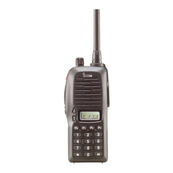
Icom IC-F3GT Service Manual
Icom marine radio user manual
Hide thumbs
Also See for IC-F3GT:
- Service manual (39 pages) ,
- Instruction manual (32 pages) ,
- Simple operation manual (3 pages)
Table of Contents
Advertisement
Advertisement
Chapters
Table of Contents

Related Manuals for Icom IC-F3GT


Summary of Contents for Icom IC-F3GT
- Page 1 SERVICE MANUAL VHF FM TRANSCEIVERS...
-
Page 2: Ordering Parts
INTRODUCTION This service manual describes the latest service information for the IC-F3GT and IC-F3GS at the time of publication. To upgrade quality, all electrical or mechanical parts and internal circuits are subject to change without notice or oblig- ation. DANGER NEVER connect the transceiver to an AC outlet or to a DC power supply that uses more than 16 V. -
Page 3: Table Of Contents
SECTION SPECIFICATIONS SECTION INSIDE VIEWS SECTION DISASSEMBLY AND OPTION INSTRUCTIONS DISASSEMBLY INSTRUCTION ..........3-1 OPTIONAL UNIT INSTALLATIONS . -
Page 4: Specifications
SECTION 1 SPECIFICATIONS Frequency coverage Type of emission Number of channels Power supply requirement at High at Low Current drain (approx.) rated audio stand-by Frequency stability Usable temperature range Dimensions (proj. not included) Weight (with BP-209) Output power Modulation system Max. -
Page 5: Section 2 Inside Views
SECTION 2 • MAIN UNIT TOP VIEW Antenna swtching circuit (D1, D2, D8: MA77) Power amplifier (Q1: 2SK2974) Low-pass filter circuit IC3A: NJM2902V Q37: DTA144EU FM IF IC (IC2: TA31136FN(D)) IF amplifier (Q14: 2SC4215 O) Mic amplifier circuit PLL IC (IC1: PD3140GS) TX/RX switch (D3, D4: MA77) -
Page 6: Section 3 Disassembly And Option Instructions
SECTION 3 DISASSEMBLY AND OPTION INSTRUCTIONS 3-1 DISASSEMBLY INSTRUCTION • REMOVING THE CHASSIS PANEL 1 Unscrew 1 nut A, and remove 1 knob B. 2 Unscrew 2 screws C. 3 Take off the chassis in the direction of the arrow. 4 Unplug J6 to separate front panel and chassis. -
Page 7: Optional Unit Installations
3-2 OPTIONAL UNIT INSTALLATIONS 1 Remove the option cover. 2 Connect one of UT-96, UT-105, UT-108, UT-109, UT-110, and UT-111 optional unit to J5. 3 Replace the option cover to the chassis-hole. Option cover Option unit 3 - 2... -
Page 8: Section 4 Circuit Description
SECTION 4 CIRCUIT DESCRIPTION 4-1 RECEIVER CIRCUITS 4-1-1 ANTENNA SWITCHING CIRCUIT Received signals are passed through the low-pass filter (L1, L2, C1–C5, C8). The filtered signals are applied to the ⁄ type antenna switching circuit (D2, D8). The antenna switching circuit functions as a low-pass filter while receiving. -
Page 9: Transmitter Circuits
4-1-5 AF CIRCUIT AF signals from the FM IF IC (IC2, pin 9) are applied to the mute switch (IC4, pin 1) via the AF filter circuit (IC3b, pins 6, 7). The output signals from pin 11 are applied to the AF power amplifier (IC5, pin 4) after being passed through the [VOL] control (R143). -
Page 10: Pll Circuits
The signal output from the power detector circuit (D32, D33) is applied to the differential amplifier (IC3a, pin 2), and the “T4” signal from the expander (IC10, pin 11), controlled by the CPU (IC8), is applied to the other input for reference. When the driving current is increased, input voltage of the differential amplifier (pin 2) will be increased. -
Page 11: Port Allocations
4-5 PORT ALLOCATIONS 4-5-1 CPU (IC8) Port Description number name Input port for battely voltage detection. RESET Input port for RESET signal. Outputs reference oscillator for the CSIFT CPU control signal. Outputs clock signal to the PLL IC (IC1), EEPROM (IC7), etc. •... -
Page 12: Section 5 Adjustment Procedures
: 10 MΩ/V DC or better AC millivoltmeter STARTING SOFTWARE ADJUSTMENT q Connect IC-F3GT/GS and PC with the optional OPC-478 and the JIG cable. w Boot up Windows, and turn the transceiver power ON. e Click the program group ‘CS-F3G ADJ’ in the ‘Programs’... - Page 13 : Reload adjustment data : Receive sensitivity measurement : Connected DC voltage : PLL lock voltage : Operating channel select : RF output power ¥ JIG cable to IC-F3GT/GS [SP] jack Connect Reload (F5) [D / A] 7.73 V BPF T1 BPF T2 1.92 V...
-
Page 14: Dc Power Supply
• Connection Standard signal generator 0.1 V to 32 mV (–127 dBm to –17 dBm) CAUTION: DO NOT transmit while an SSG is connected to the antenna connector. Attenuator deviation meter 40 dB or 50 dB RF power meter 0.1–10 W/50 Frequency counter ¥... -
Page 15: Pll Adjustment
5-2 PLL ADJUSTMENT ADJUSTMENT ADJUSTMENT CONDITIONS PLL LOCK • Operating frequency VOLTAGE 136.000 MHz (L-band) 146.000 MHz (H-band) • Receiving • Transmitting • MAIN unit RF power meter PLL lock voltage adjustment PLL lock voltage check point MEASUREMENT UNIT LOCATION MAIN Connect a digital multi meter to check point Bottom view... -
Page 16: Software Adjustment
5-3 SOFTWARE ADJUSTMENT Select an operation using [ ] / [ ] keys, then set specified value using [ ] / [ ] keys on the connected computer keyboard. ADJUSTMENT ADJUSTMENT CONDITION REFERENCE • Operating frequency: FREQUENCY [TXF] • High/Low switch •... - Page 17 SOFTWARE ADJUSTMENT – continued Select an operation using [ ] / [ ] keys, then set specified value using [ ] / [ ] keys on the connected computer keyboard. ADJUSTMENT ADJUSTMENT CONDITION 1 • Operating frequency: SENSITIVITY [BPF T1] – [BPF T4] •...
-
Page 18: Main Unit
SECTION 6 PARTS LIST [MAIN UNIT] ORDER DESCRIPTION 1130007610 S.IC µPD3140GS-E1 (DS8) 1110003490 S.IC TA31136FN (D,EL) 1110003780 S.IC NJM2902V-TE1 1130008090 S.IC BU4066BCFV-E1 1110001810 S.IC TA7368F (TP1) 1110005350 S.IC NJM2870F05-TE1 1180001740 S.IC TK11250BMCL 1130009680 S.IC HN58X2432TI 1140008650 S.IC HN58X2464TI 1140010000 S.IC HD6433876B50H IC10 1190000350 S.IC... - Page 19 [MAIN UNIT] ORDER DESCRIPTION ERJ3GEYJ 101 V (100 Ω) 7030003320 S.RESISTOR 7030003560 S.RESISTOR ERJ3GEYJ 103 V (10 kΩ) ERJ3GEYJ 270 V (27 Ω) 7030003250 S.RESISTOR ERJ3GEYJ 680 V (68 Ω) 7030003300 S.RESISTOR ERJ3GEYJ 820 V (82 Ω) [OTHER] 7030003310 S.RESISTOR 7030003450 S.RESISTOR ERJ3GEYJ 122 V (1.2 kΩ) 7030003500 S.RESISTOR...
- Page 20 [MAIN UNIT] ORDER DESCRIPTION R171 7030003640 S.RESISTOR ERJ3GEYJ 473 V (47 kΩ) R174 7030003580 S.RESISTOR ERJ3GEYJ 153 V (15 kΩ) R175 7030003440 S.RESISTOR ERJ3GEYJ 102 V (1 kΩ) R176 7030003510 S.RESISTOR ERJ3GEYJ 392 V (3.9 kΩ) R177 7030003440 S.RESISTOR ERJ3GEYJ 102 V (1 kΩ) R178 7030003510 S.RESISTOR ERJ3GEYJ 392 V (3.9 kΩ)
- Page 21 [MAIN UNIT] ORDER DESCRIPTION 4550006200 S.TANTALUM ECST0JY106R 4030007090 S.CERAMIC C1608 CH 1H 470J-T-A 4030007050 S.CERAMIC C1608 CH 1H 220J-T-A 4030007040 S.CERAMIC C1608 CH 1H 180J-T-A 4030006860 S.CERAMIC C1608 JB 1H 102K-T-A 4030006900 S.CERAMIC C1608 JB 1H 103K-T-A 4030006900 S.CERAMIC C1608 JB 1H 103K-T-A 4030006860 S.CERAMIC C1608 JB 1H 102K-T-A 4030007020 S.CERAMIC...
- Page 22 [MAIN UNIT] ORDER DESCRIPTION C221 4030008910 S.CERAMIC C1608 JB 1H 393K-T-A C222 4030011600 S.CERAMIC C1608 JB 1E 104K-T-N C223 4030006900 S.CERAMIC C1608 JB 1H 103K-T-A C224 4030006900 S.CERAMIC C1608 JB 1H 103K-T-A C225 4030006880 S.CERAMIC C1608 JB 1H 472K-T-A 4030009880 S.CERAMIC C1608 JB 1H 682K-T-A C227 4030008920 S.CERAMIC...
-
Page 23: Section 7 Mechanical Parts And Disassembly
SECTION 7 [CHASSIS PARTS] REF. NO. ODER NO. DESCRIPTION 8210016541 2251 T-front panel-1 8210016671 2251 S-front panel-1 8930050890 2251 terminal holder 8010017991 2251 chassis-1 8210016570 2251 rear panel 8930050870 2251 release button 8210016560 2251 PTT panel 8310047580 2251 window plate 8930051350 2251 jack rubber 8210016550 2251 jack panel MP10... - Page 24 MP33 (C) MP26 (C) MP39 (C) MP32 (C) MP32 (C) MP23 (C) MP31 (C) MP4 (C) MP3 (C) MP15 (C) MP25 (C) MP2 (C) MP5 (C) MP12 (C) MP31 (C) MP14 (C) MP5 (M) MP36 (C) MP38 (C) MP8 (C) MP9 (C) MP31 (C) MP40 (C)
-
Page 25: Semi-Conductor Information
SECTION 8 SEMI-CONDUCTOR INFORMATION • TRANSISTOR AND FET’S 2SA1577 Q 2SB1132 R 2SC4116 GR (Symbol: HQ) (Symbol: BARB) (Symbol: LG) 2SK1069 4 2SK2973 2SK2974 (Symbol: FJ4) (Symbol: K1) (Symbol: K2974) (top view) DTA144 EUA DTC144 EUA 3SK320 (Symbol: U7) (Symbol: 16) (Symbol: 26) XP6501 AB XP1213... -
Page 26: Section 9 Board Layouts
SECTION 9 BOARD LAYOUTS 9-1 GENERAL AND EIA/TIA VERSIONS (EXCEPT W/N-TYPE) • MAIN UNIT (TOP VIEW) 9 - 1 C294 C293 C303 R253 C115 C300 C111 R264 R175 R185 C124 R177 C217 C131 C148 C136 R114 C213 R115 R107 R117 C214 R113 C128... - Page 27 • MAIN UNIT (BOTTOM VIEW) C155 C174 R261 C158 R143 C173 C114 C281 C106 C298 C285 C105 C287 C104 R159 C101 C288 R154 C204 C168 R187 C277 C165 R252 C167 C166 R132 R191 C221 R190 C123 R229 C244 R230 R150 R231 IC10 C229...
-
Page 28: Ets/Cept Version
9-2 ETS/CEPT VERSION • MAIN UNIT (TOP VIEW) 9 - 3 C294 C293 C303 R253 C115 C300 C111 R264 R175 R185 C124 R177 C217 C131 C148 C136 R114 C213 R115 R107 R117 C214 R113 C128 R112 R204 C299 C156 R135 C119 C120 C122... - Page 29 • MAIN UNIT (BOTTOM VIEW) C155 C174 R261 C158 R143 C173 C114 C306 C281 C106 C284 C298 C285 C105 C287 C104 R159 C101 C288 R154 C204 C168 R187 C277 C165 R252 C167 C166 R132 R191 C221 R190 C123 R229 C244 R230 R150 R231...
-
Page 30: W/N-Type
9-3 W/N-TYPE • MAIN UNIT (TOP VIEW) 9 - 5 R269 R244 C293 C303 R253 C115 C300 C111 R264 R175 R185 C124 R177 C217 C131 C148 C136 R114 C213 R115 R107 R117 C214 R113 C128 R112 R204 C299 C158 R135 C119 C120 C122... - Page 31 • MAIN UNIT (BOTTOM VIEW) C155 C174 R261 C161 C114 C281 C106 C298 C285 C105 C287 C104 R159 C101 C288 R154 C204 C168 R187 C165 C277 R252 C167 C166 R132 R191 C221 R190 C123 R229 C244 R230 R150 R231 IC10 C229 R223 C235...
-
Page 32: Parts List
SECTION 10 10-1 PARTS LIST [MAIN UNIT] REF. NO. ODER NO. DESCRIPTION 1520000650 S.TRANSISTOR 2SB1201-S-TL 1590000480 S.TRANSISTOR RN2402 (TE85R) 1590000510 S.TRANSISTOR RN1409 (TE85R) 1530001950 S.TRANSISTOR 2SC2712-GR (TE85R) 1750000550 S.DIODE 1SS355 TE-17 1750000020 S.DIODE 1SS184 (TE85R) 1790000950 S.ZENER MA8056-M (TX) 7030010000 S.RESISTOR MCR10EZHF 24R0 7030010000 S.RESISTOR MCR10EZHF 24R0... -
Page 33: Voltage Diagram
10-3 VOLTAGE DIAGRAM 13.77 V 10-4 BOARD LAYOUT 12.49 V 12.47 V 13.80 V R1 24 R5 10 k 2SB1201 S R2 24 11.82 V 11.80 V 13.63 V 12.46 V RN2404 DS1 TLG124A R4 10 k 0.23 V 1SS355 0.22 V 56 k RN1409... -
Page 34: Block Diagram
SECTION 11 BLOCK DIAGRAM J5 AXN330C038 CR-664A [OTHER] CR-671A A, D (15.3 MHz) OPTION UNIT 2TONE or 5TONE MIC, AF, PTT, MMUT RMUT, AFONOP SIGOUT CONT Q17 UN911H Q15 2SB1132 R Q16 XP6501 AB D26 DAN202K IC5 TA7368F IC10 M62363FP-650C EXT.MIC MIC JACK Q31 DTC144TU... - Page 35 SECTION 12 VOLTAGE DIAGRAM AFOUT DISCIN AXN330C038 OPV1 OPV2 OPV3 CIRQ BUSY OPT3 OPT2 AFOUT OPT1 to Optional unit DISCIN SIGOUT RXMUTE RMUTE CPU5 MOWN BEEPOUT R131 BUSY AFONOP MICMUTE MMUTE MICIN MICOUT TX: 4.84 V UN911H PTTOUT RX: 0 V PTTIN C147 C154...
- Page 36 AFOUT DISCIN VOLMIN — VOLMAX 3.31 V 7.23 V — 7.07 V TA7368F 2SB1132 R POUT TX: 0 V PWGND 4.62 V RX: 3.96 V PREGND PHASE 7 NF 6 R126 RIPPLE 94 V XP6501 AB 10 k R120 68 k R127 R122 2.7 k...
- Page 37 4.03 V TX: 4.62 V 3.37 V RX: 0.04 V 0.1 H 0.001 4.7 k 0.1 H 3.3 k TX: 0.7 V 0.001 RX: 0.73 V 2SC5085 Y MA77 27 P 1.2 k MA77 82 nH TX: 0.8 V RX: 0 V C4215 O 27 K 68 A...
- Page 38 SECTION 12 VOLTAGE DIAGRAM AFOUT DISCIN AXN330C038 OPV1 OPV2 OPV3 CIRQ BUSY OPT3 OPT2 AFOUT OPT1 DISCIN to Optional unit SIGOUT RXMUTE RMUTE R177 MOWN CPU5 C125 BEEPOUT C132 IC3C R266 0.0022 BU4066BCFV BUSY R131 15 k 0.0056 NJM2902V AFONOP TX: 3.69 V C217 C124...
- Page 40 S-13713IZ-C1V-q 1-1-32, Kamiminami, Hirano-ku, Osaka, 547-0003, Japan © 2000 Icom Inc.
- Page 41 SERVICE MANUAL UHF FM TRANSCEIVERS...
- Page 42 INTRODUCTION This service manual describes the latest service information for the IC-F4GT and IC-F4GS at the time of publication. To upgrade quality, all electrical or mechanical parts and internal circuits are subject to change without notice or oblig- ation. DANGER NEVER connect the transceiver to an AC outlet or to a DC power supply that uses more than 16 V.
- Page 43 SECTION SPECIFICATIONS SECTION INSIDE VIEWS SECTION DISASSEMBLY AND OPTION INSTRUCTIONS DISASSEMBLY INSTRUCTION ..........3-1 OPTIONAL UNIT INSTALLATIONS .
- Page 44 SECTION 1 SPECIFICATIONS Frequency coverage Type of emission Number of channels Power supply requirement at High at Low Current drain (approx.) rated audio stand-by Frequency stability Usable temperature range Dimensions (proj. not included) Weight (with BP-209) Output power Modulation system Max.
-
Page 45: Section 2 Inside Views
SECTION 2 • MAIN UNIT TOP VIEW Antenna switcing circuit (D2, D8: MA77) Power amplifier (Q1: 2SK2974) IC3A: NJM3403AV Q37: DTA144EU IF amplifier (Q14: 2SC4215 O) PLL IC (IC1: PD3140GS) TX/RX switch (D3, D4: MA77) Mic amplifier circuit INSIDE VIEWS 2 - 1 BOTTOM VIEW Antenna switcing circuit... -
Page 46: Section 3 Disassembly And Option Instructions
SECTION 3 DISASSEMBLY AND OPTION INSTRUCTIONS 3-1 DISASSEMBLY INSTRUCTION • REMOVING THE CHASSIS PANEL 1 Unscrew 1 nut A, and remove 1 knob B. 2 Unscrew 2 screws C. 3 Take off the chassis in the direction of the arrow. 4 Unplug J6 to separate front panel and chassis. -
Page 47: Optional Unit Installations
3-2 OPTIONAL UNIT INSTALLATIONS 1 Remove the option cover. 2 Connect one of UT-96, UT-105, UT-108, UT-109, UT-110, UT-111, and UT-113 optional units to J5. 3 Replace the option cover to the chassis-hole. Option cover Option unit 3 - 2... -
Page 48: Section 4 Circuit Description
SECTION 4 CIRCUIT DESCRIPTION 4-1 RECEIVER CIRCUITS 4-1-1 ANTENNA SWITCHING CIRCUIT The antenna switching circuit functions as a low-pass filter while receiving. However, its impedance becomes very high while D2 and D8 are turned ON. Thus transmit signals are blocked from entering the receiver circuits. The antenna switching circuit employs a ⁄... -
Page 49: Transmitter Circuits
4-1-5 AF CIRCUIT AF signals from the FM IF IC (IC2, pin 9) are applied to the mute switch (IC4, pin 1) via the AF filter circuit (IC3b, pins 6, 7). The output signals from pin 11 are applied to the AF power amplifier (IC5, pin 4) after being passed through the [VOL] control (R143). -
Page 50: Pll Circuits
The signal output from the power detector circuit (D32, D33) is applied to the differential amplifier (IC3a, pin 2), and the “T4” signal from the expander (IC10, pin 11), controlled by the CPU (IC8), is applied to the other input for reference. When the driving current is increased, input voltage of the differential amplifier (pin 2) will be increased. - Page 51 4-5 PORT ALLOCATIONS 4-5-1 CPU (IC8) Port Description number name Input port for battely voltage detection. RESET Input port for RESET signal. Outputs reference oscillator for the CSIFT CPU control signal. Outputs clock signal to the PLL IC (IC1), EEPROM (IC7), etc. •...
-
Page 52: Section 5 Adjustment Procedures
SECTION 5 ADJUSTMENT PROCEDURES 5-1 PREPARATION When you adjust the contents on page 5-5 or 5-6, SOFTWARE ADJUSTMENT, the optional CS-F3G ADJ (Rev. 2.0 or later), OPC-478 CLONING CABLE REQUIRED TEST EQUIPMENT EQUIPMENT GRADE AND RANGE Output voltage DC power supply Current capacity Measuring range RF power meter... - Page 53 SCREEN DISPLAY EXAMPLE CS-F3G ADJ Rev.2.0 File Option COM 1: OPEN [A / D] : 197 : C5h : TEMPS : 190 : BEh : 32.23 ’C LVIN : 98 : 62h : REMOT : 14 : 0Eh : BDET : 255 : FFh : CH No.
- Page 54 CONNECTION Standard signal generator 0.1 V to 32 mV ( 127 dBm to 17 dBm) CAUTION: DO NOT transmit while an SSG is connected to the antenna connector. Attenuator deviation meter 40 dB or 50 dB RF power meter 0.1 10 W/50 Frequency counter DC POWER CABLE CONNECTIONS...
-
Page 55: Pll Adjustment
5-2 PLL ADJUSTMENT ADJUSTMENT ADJUSTMENT CONDITIONS PLL LOCK • Operating frequency: VOLTAGE 400.000 MHz 440.000 MHz 470.000 NHz 490.000 MHz • Receiving • Transmitting • Operating frequency: 430.000 MHz 470.000 MHz 500.000 MHz 512.000 MHz 520.000 MHz • Receiving • Transmitting : 400–430 MHz : 440–470 MHz ˆ... -
Page 56: Software Adjustment
5-3 SOFTWARE ADJUSTMENT Select an operation using [ ] / [ ] keys, then set specified value using [ ] / [ ] keys on the connected computer keyboard. ADJUSTMENT ADJUSTMENT CONDITION REFERENCE • Operating frequency: FREQUENCY [TXF] • High/Low switch •... - Page 57 SOFTWARE ADJUSTMENT – continued Select an operation using [ ] / [ ] keys, then set specified value using [ ] / [ ] keys on the connected computer keyboard. ADJUSTMENT ADJUSTMENT CONDITION 1 • Operating frequency: SENSITIVITY [BPF T1] – [BPF T4] •...
-
Page 58: Parts List
SECTION 6 PARTS LIST [MAIN UNIT] ORDER DESCRIPTION 1130007610 S.IC µPD3140GS-E1 (DS8) 1110003490 S.IC TA31136FN (D,EL) 1110005140 S.IC NJM3403AV-TE1 1130008090 S.IC BU4066BCFV-E1 1110001810 S.IC TA7368F (TP1) 1110005350 S.IC NJM2870F05-TE1 1180001740 S.IC TK11250BMCL 1130009680 S.IC HN58X2432TI 1140008650 S.IC HN58X2464TI 1140010000 S.IC HD6433876B50H IC10 1190000350 S.IC... - Page 59 [MAIN UNIT] ORDER DESCRIPTION L441 6200003960 S.COIL MLF1608A 1R0K-T L442 6200004720 S.COIL MLF1608D R10K-T L443 6200006190 S.COIL BLM21P300S 7030003670 S.RESISTOR ERJ3GEYJ 823 V (82 kΩ) 7030003580 S.RESISTOR ERJ3GEYJ 153 V (15 kΩ) 7030003580 S.RESISTOR ERJ3GEYJ 153 V (15 kΩ) ERJ2GEJ 101 X (100 Ω) 7030004980 S.RESISTOR 7030005050 S.RESISTOR ERJ2GEJ 103 X (10 kΩ)
- Page 60 [MAIN UNIT] ORDER DESCRIPTION R194 7030003680 S.RESISTOR ERJ3GEYJ 104 V (100 kΩ) R195 7030003680 S.RESISTOR ERJ3GEYJ 104 V (100 kΩ) R196 7030003680 S.RESISTOR ERJ3GEYJ 104 V (100 kΩ) R197 7030003720 S.RESISTOR ERJ3GEYJ 224 V (220 kΩ) R198 7030003590 S.RESISTOR ERJ3GEYJ 183 V (18 kΩ) R199 7030003640 S.RESISTOR ERJ3GEYJ 473 V (47 kΩ)
- Page 61 [MAIN UNIT] ORDER DESCRIPTION 4550006540 S.TANTALUM ECST1CY475R 4030007000 S.CERAMIC C1608 CH 1H 090D-T-A 4030007010 S.CERAMIC C1608 CH 1H 100D-T-A 4030007020 S.CERAMIC C1608 CH 1H 120J-T-A 4030006850 S.CERAMIC C1608 JB 1H 471K-T-A 4030009530 S.CERAMIC C1608 CH 1H 030B-T-A 4030009910 S.CERAMIC C1608 CH 1H 040B-T-A 4030017460 S.CERAMIC ECJ0EB1E102K 4030009920 S.CERAMIC...
- Page 62 [MAIN UNIT] ORDER DESCRIPTION C173 4510004640 S.ELECTROLYTIC ECEV1CA470SP 4550006760 S.TANTALUM TEMSVB2 1A 336M-8R C174 4510005430 S.ELECTROLYTIC ECEV0JA220SR C179 4030006900 S.CERAMIC C1608 JB 1H 103K-T-A C193 4030006990 S.CERAMIC C1608 CH 1H 080D-T-A C194 4030007020 S.CERAMIC C1608 CH 1H 120J-T-A C195 4030007080 S.CERAMIC C1608 CH 1H 390J-T-A C196 4030006850 S.CERAMIC...
- Page 63 [MAIN UNIT] ORDER DESCRIPTION C666 4030009910 S.CERAMIC C1608 CH 1H 040B-T-A 4030009920 S.CERAMIC C1608 CH 1H 050B-T-A C668 4030009530 S.CERAMIC C1608 CH 1H 030B-T-A C669 4030014180 S.CERAMIC ECUE1H470JCQ C670 4030006850 S.CERAMIC C1608 JB 1H 471K-T-A 4030017730 S.CERAMIC ECJ0EB1E471K C672 4030014180 S.CERAMIC ECUE1H470JCQ C673 4030014180 S.CERAMIC...
- Page 64 SECTION 7 [CHASSIS PARTS] REF. NO. ODER NO. DESCRIPTION 8210016541 2251 T-front panel-1 8210016671 2251 S-front panel-1 8930050890 2251 terminal holder 8010017991 2251 chassis-1 8210016570 2251 rear panel 8930050870 2251 release button 8210016560 2251 PTT panel 8310047580 2251 window plate 8930051350 2251 jack rubber 8210016550 2251 jack panel MP10...
- Page 65 MP37 (C) MP42 (C) MP10 (C) MP27 (C) SP1 (M) MP1 (C) MP21 (C) MP20 (C) MP24 (C) MP7 (C) MP13 (C) UNIT abbreviation (C): CHASSIS PARTS, (M): MAIN UNIT 7 - 2 MP12 (C) MP5 (M) MP8 (M) MP31 (C) MP6 (M) MP1 (M) MP32 (C)
- Page 66 SECTION 8 SEMI-CONDUCTOR INFORMATION • TRANSISTOR AND FET’S 2SA1577 Q 2SB1132 R 2SC3585 R44 (Symbol: HQ) (Symbol: BARB) (Symbol: R44) 2SC5085 Y 2SC5107 O 2SK2973 (Symbol: MCY) (Symbol: MFO) (Symbol: K1) 3SK239 A DTA144 EU DTC144 EE (Symbol: 16) (Symbol: XR) (Symbol: 26) UN911 H XP1213...
-
Page 67: Section 9 Board Layouts
SECTION 9 BOARD LAYOUTS 9-1 LOW BAND • MAIN UNIT (TOP VIEW) 9 - 1 R512 R473 R526 C218 C491 R529 C111 Q402 R511 L406 R421 R422 R420 R184 L407 C571 C674 R257 C673 R185 EP14 C233 R508 R168 L441 C212 C213 R107... - Page 68 • MAIN UNIT (BOTTOM VIEW) C155 C174 R261 C158 C669 C173 C114 R469 C110 C450 R162 C106 C243 C105 R464 C104 R159 R449 C555 R448 C666 C168 C100 C406 C165 R404 EP10 C211 C123 R519 R230 IC10 R154 R165 R153 C565 R164 R152...
-
Page 69: 440-470 Mhz Band Except W/N-Type
9-2 440–470 MHz BAND EXCEPT W/N-TYPE • MAIN UNIT (TOP VIEW) 9 - 3 R512 R473 R526 C218 C491 R529 C111 Q402 R511 L406 R421 R422 R420 R184 L407 C571 C674 C673 R185 EP14 C233 R508 R168 L441 C212 C213 R107 C672 C214... - Page 70 • MAIN UNIT (BOTTOM VIEW) C174 C155 R261 C158 C669 C173 C114 R469 C110 C450 R162 C106 C243 C105 R464 C104 R159 R449 C555 R448 C666 C168 C100 C406 C165 R404 EP10 C211 R519 C123 R230 IC10 R154 R165 R153 C565 R164 R152...
-
Page 71: 470-500 Mhz And High Bands
9-3 470–500 MHz AND HIGH BANDS • MAIN UNIT (TOP VIEW) 9 - 5 R512 R473 R526 C218 C491 R529 C111 Q402 L406 R511 R421 R422 R420 R184 C571 L407 C674 R257 C673 R185 EP14 C233 R508 R168 L441 C212 C213 R107 C672... - Page 72 • MAIN UNIT (BOTTOM VIEW) C174 C155 R261 C158 C669 C173 C114 R469 C110 C450 R162 C106 C243 C105 R464 C104 R159 R449 C555 R448 C666 C168 C100 C406 C165 R404 EP10 C211 C123 R519 R230 IC10 R165 R154 R153 R164 C565 R152...
-
Page 73: W/N-Type
9-4 W/N-TYPE • MAIN UNIT (TOP VIEW) 9 - 7 R512 R473 R526 C218 C491 R529 C111 Q402 R511 L406 R421 R422 R420 R184 L407 C571 C674 R257 C673 R185 EP14 C233 R508 R168 L441 C212 C213 R107 C672 C214 R113 R112 C128... - Page 74 • MAIN UNIT (BOTTOM VIEW) C174 C155 R261 C158 C669 C114 R469 C110 C450 R162 C106 C243 C105 R464 C104 R159 R449 C555 R448 C666 C168 C100 C406 C165 R404 EP10 C211 C123 R519 R230 IC10 R154 R165 R153 R164 C565 R152 R417...
-
Page 75: Parts List
SECTION 10 10-1 PARTS LIST [MAIN UNIT] REF. NO. ODER NO. DESCRIPTION 1520000650 S.TRANSISTOR 2SB1201-S-TL 1590000480 S.TRANSISTOR RN2402 (TE85R) 1590000510 S.TRANSISTOR RN1409 (TE85R) 1530001950 S.TRANSISTOR 2SC2712-GR (TE85R) 1750000550 S.DIODE 1SS355 TE-17 1750000020 S.DIODE 1SS184 (TE85R) 1790000950 S.ZENER MA8056-M (TX) 7030010000 S.RESISTOR MCR10EZHF 24R0 7030010000 S.RESISTOR MCR10EZHF 24R0... -
Page 76: Voltage Diagram
10-3 VOLTAGE DIAGRAM 13.77 V 10-4 BOARD LAYOUT 12.49 V 12.47 V 13.80 V R1 24 R5 10 k 2SB1201 S R2 24 11.82 V 11.80 V 13.63 V 12.46 V RN2404 DS1 TLG124A R4 10 k 0.23 V 1SS355 0.22 V 56 k RN1409... -
Page 77: Block Diagram
SECTION 11 BLOCK DIAGRAM J5 AXN330C038 OPTION UNIT 2TONE or 5TONE X4 CR-662 (15.3 MHz) MIC, AF, PTT, MMUT RMUT, AFONOP SIGOUT CONT Q17 UN911H Q15 2SB1132 R Q16 XP6501 AB D26 DAN202K IC5 TA7368F IC10 M62363FP-650C EXT.MIC MIC JACK Q31 DTC144TU AF OUT D27 RB706F-40... - Page 78 SECTION 12 VOLTAGE DIAGRAM AFOUT DISCIN AXN330C038 CPU5 OPV1 CPU5 OPV2 OPV3 CIRQ CPU5 OPT3 OPT2 AFOUT OPT1 Tx: 4.79 V to Optional unit DISCIN Rx: 0.00 V SIGOUT RXMUTE RMUTE MOWN BEEPOUT C554 BUSY 470 P AFONOP MICMUTE BUSY MMUTE R510 MICIN...
- Page 79 AFOUT DISCIN CPU5 CPU5 AFON AF min 7.23 V AF max 7.03 V TA7368F 3.31 V 2SB1132 R POUT PWGND Tx: 2.20 V PREGND Rx: 2.21 V PHASE 7 AFON NF 6 R126 RIPPLE 3.96 V 10 k R127 R122 R120 2.7 k R178...
- Page 80 C471 47 P 10 k R445 C670 470 P C472 47 P L411 10 nH C Tx: 3.64 V 27 nH B 12 nH J Rx: 0.19 V 15 nH F 22 nH [OTHER] 18 nH K 22 nH B 4.7 k 0.001 470 P...
- Page 81 SECTION 12 VOLTAGE DIAGRAM AFOUT DISCIN AXN330C038 CPU5 OPV1 CPU5 OPV2 OPV3 CIRQ CPU5 OPT3 Tx: 2.19 V OPT2 Rx: 2.20 V AFOUT OPT1 Tx: 2.19 V 2.5 Vp-p to Optional unit DISCIN Tx: 4.79 V C556 4 Vp-p Rx: 2.20 V ( a)1 kHz, –1.5 kHz) SIGOUT Rx: 0.00 V...
- Page 83 S-13713IZ-C1U-1 1-1-32, Kamiminami, Hirano-ku, Osaka, 547-0003, Japan © 2000 Icom Inc.
Need help?
Do you have a question about the IC-F3GT and is the answer not in the manual?
Questions and answers