JVC KD-S621 Service Manual
Cd receiver
Hide thumbs
Also See for KD-S621:
- Instructions manual (22 pages) ,
- Installation & connection manual (4 pages) ,
- Service manual (49 pages)
Advertisement
Quick Links
Download this manual
See also:
Instruction Manual
SERVICE MANUAL
Contents
Safety precaution
Preventing static electricity
Disassembly method
Adjustment method
CD RECEIVER
KD-S621
LOUD
SEL
DISP
7
9
10
11
8
MO
RPT
1-2
1-3
1-4
1-11
COPYRIGHT
2002 VICTOR COMPANY OF JAPAN, LTD.
FM
CD
¢
SSM
4
AM
12
RND
MODE
SCM
E -------- Continental Europe
EX ------------ Central Europe
Flow of functional
operation unit TOC read
Maintenance of laser pickup
Replacement of laser pickup
Description of major ICs
KD-S621
Area Suffix
1-12
1-14
1-14
1-15 26
No.49675
Jan. 2002
Advertisement

Related Manuals for JVC KD-S621


Summary of Contents for JVC KD-S621
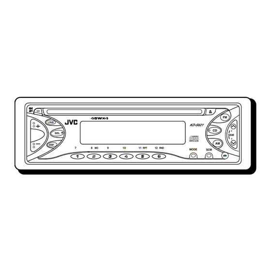
- Page 1 KD-S621 SERVICE MANUAL CD RECEIVER KD-S621 LOUD ¢ DISP MODE Area Suffix E -------- Continental Europe EX ------------ Central Europe Contents Safety precaution Flow of functional Preventing static electricity operation unit TOC read 1-12 Disassembly method Maintenance of laser pickup...
- Page 2 KD-S621 Preventing static electricity 1.Grounding to prevent damage by static electricity Electrostatic discharge (ESD), which occurs when static electricity stored in the body, fabric, etc. is discharged, can destroy the laser diode in the traverse unit (optical pickup). Take care to prevent this when performing repairs.
-
Page 3: Disassembly Method
KD-S621 Disassembly method <Main body> Removing the front panel assembly (See Fig.1) Press the eject button in the lower right part of the front panel. Remove the front panel assembly from the body. Front panel assembly Eject button Fig.1 Tab a Removing the front chassis assembly (See Fig.2 and 3) - Page 4 KD-S621 Removing the heat sink (See Fig.4) Remove the three screws A on the left side of the body. Heat sink Fig.4 Joints b Removing the bottom cover (See Fig.5 and 6) Bottom cover Prior to performing the following procedure, remove the front panel assembly, the front chassis assembly and the heat sink.
- Page 5 KD-S621 Removing the main board (See Fig.7 and 8) Prior to performing the following procedure, remove the front panel assembly, the front chassis assembly, the heat sink and the bottom cover. Remove the screw B, the four screws C and the...
- Page 6 KD-S621 Removing the control switch board (See Fig.10 to 12) Prior to performing the following procedure, remove the front panel assembly. Remove the four screws G attaching the rear cover on the back of the front panel assembly. Unjoint the nine joints c with the front panel and the Rear cover rear cover.
- Page 7 KD-S621 Damper bracket Removing the CD mechanism control CD mechanism ass’y board(See Fig.1 and 2) Unsolder the part f and g on the CD mechanism control board. Remove the stator fixing the CD mechanism control board and the damper bracket (To remove the stator smoothly, pick up the center part).
- Page 8 KD-S621 Removing the loading motor Loading motor (See Fig.3 to 5) Prior to performing the following procedure, remove the CD mechanism control board. Belt Remove the two springs k attaching the CD mechanism ass’y and the front bracket. Fig.5 Remove the two screws G and the front bracket while pulling the flame outward.
- Page 9 KD-S621 Removing the feed motor ass’y Part n FD screw (See Fig.10) Feed motor ass’y Prior to performing the following procedure, remove the CD mechanism control board, the front bracket Part O (loading motor) and the CD mechanism ass’y. Remove the two screws K and the feed motor ass’y.
-
Page 10: Adjustment Method
Frequency Band 6. Digital tester FM 87.5MHz ~ 108.0MHz 7. Tracking offset meter MW 522kHz ~ 1620 kHz 8. Test Disc JVC :CTS-1000 LW 144kHz ~ 279kHz 9. Extension cable for check EXTGS004-26P 1 Dummy load Exclusive dummy load should be used for AM,and FM. For FM dummy load,there is a loss of 6dB between SSG output and antenna input.The loss of 6dB need not be considered... - Page 11 KD-S621 Flow of functional operation until TOC read Power ON • When the laser diode correctly Set Function to CD • When the pickup correctly moves emits to the inner area of the disc Microprocessor Microprocessor Disc inserted commands commands TC9462 "53"...
- Page 12 KD-S621 Feed Section Check CD 9V Is the voltage output at Is the wiring for IC521 Is 5V present at IC581 and 5V. IC521 pin "53" 5V or 0V? (90) ~ (100) correct? pin "11"? Check the vicinity of IC521.
- Page 13 KD-S621 Maintenance of laser pickup (1) Cleaning the pick up lens Before you replace the pick up, please try to clean the lens with a alcohol soaked cotton swab. (2) Life of the laser diode When the life of the laser diode has expired, the following symptoms will appear.
-
Page 14: Description Of Major Ics
KD-S621 Description of major ICs HA13164A(IC901) : Regulator 1.Pin layout 1 2 3 4 5 6 7 8 9 10 11 12 13 14 15 2.Block diagram 100u 0.1u BATT.DET OUT ANT OUT Surge Protector 0.1u EXT OUT COMPOUT BIAS 0.1u... - Page 15 KD-S621 AN8806SB-W (IC501) : RF & Servo amp. 1.Pin layout 36 PDAC PD 1 35 PDBD LD 2 34 PDF LDON 3 33 PDE LDP 4 VCC 5 32 PDER RF- 6 31 PDFR RF OUT 7 30 TBAL 29 FBAL...
- Page 16 KD-S621 3. Pin function AN8806SB-W Pin No. Symbol Function APC amp . Input terminal APC amp . Output terminal LD ON LD ON/OFF control terminal Connect to GND Power supply RF amp . Reversing input terminal RFamp . Output terminal...
- Page 17 KD-S621 LA4743K(IC321):Power AMP 1.Block diagram 2200 F 0.022 F Vcc 1/2 Vcc 3/4 IN 1 OUT 1+ 0.22 F OUT 1- PWR GND1 Protective circuit OUT 2+ IN 2 OUT 2- 0.22 F PWR GND2 ST BY Stand by Switch...
- Page 18 KD-S621 2.Terminal layout 3.Pin function LA4743K Pin No. Symbol Function Header of IC Power GND Outpur(-) for front Rch OUTRR- STBY Stand by input OUTRR+ Output (+) for front Rch VCC1/2 Power input OUTRF- Output (-) for rear Rch Power GND...
- Page 19 KD-S621 LA6567H-X(IC541):CD DRIVE 1.Pin layout & blockdiagram CH 3,4,5 Thermal shutdown VCC2 Power supply V05- V05+ S-GND V04+ VCONT V04- VIN4 V03+ VIN4G Signal system power supply V03- VCC-S VC2+ VREF-IN 5VREG(PNPTr The outside puuting) V02- REG-OUT V01+ REG-IN V01-...
- Page 20 KD-S621 2. Pin function LA6567H-X(2/2) Pin no. Symbol Function VCC2 CH3,4,5 Power supply( It is short with VCC1,VCC-S) V05- Loading output(-) V05+ Loading terminal (+) V04+ CH4 Output terminal(+) V04- CH4 Output terminal(-) V03+ CH3 Output terminal(+) V03- CH3 Output terminal(-)
- Page 21 KD-S621 LC72366-9A73 (IC801) : System CPU 1. Pin layout 2. Pin function Pin No. Symbol Function Crystal oscillator input port Connect to ground TEST2 J-BUS SI No use J-BUS SO No use No use J-BUS SCK No use J-BUS I/O...
- Page 22 KD-S621 LC72366-9A73(2/2) Pin No. Port Name Function CD 8V supply on CD ON 5V power contorl RELAY Sub-code/block/clock signal output BLKCK No use BEEP CD mechanism detect switch CD mechanism detect switch CD mechanism detect switch CD pickup rest position...
- Page 23 KD-S621 LC75823W (IC601) : LCD driver 1. Pin Layout & Symbol 64 63 62 61 60 59 58 57 56 55 54 53 52 51 50 49 17 18 19 20 21 22 23 24 25 26 27 28 29 30 31 32 2.
- Page 24 KD-S621 TEA6320T-X (IC301) : E.volume 1.Pin layout 2.Block diagram VOLUME 2 MUTE 0 to 55 dB FUNCTION BALANCE OUTRR OUTLR ZERO CROSS FENDER REAR POWER DETECTOR OUTRF OUTLF SUPPLY VOLUME 1 BASS TREBLE +20 to -31 dB VOLUME 2 LEFT...
- Page 25 KD-S621 NJM4565M-WE (IC151) : Ope. amp A OUTPUT B OUTPUT A INPUT A INPUT B INPUT B INPUT 1-26...
-
Page 26: Block Diagram
KD-S621 Block diagram CJ701 TU701 CJ302 TU.LCH FM/AM LINE OUT TU.RCH TUNER REST REST FM/AM MONO SWITCH LOADING FM.OSC SPINDLE IC321 IC301 IC541 CD,SENSE IC561 FEED POWER CD,RESET E.VOL LOADING SERVO LOADING LOADING TRACKING S.METER STATUS MOTOR FOCUS & SD/ST... - Page 27 KD-S621 KD-S621 Standard schematic diagrams Main amp section TU701 QAU0257-001 CJ701 QNB0100-002 L701 Q861 DTA114EKA-X 4.7u MUTE R201 R703 R101 R701 R333 R334 D332 R336 Q332 2SD1781K/QR/-X 2.2k Q791 1SS355-X 2SB1197K/QR/-X R731 R702 R704 D333 R436 Q432 1.5k R791 2.2k...
- Page 28 KD-S621 CD servo & control section D551 DSK10C-T1 REST C543 C541 0.033 22/16 IC561 Q541 2SA1706/ST/-T MN6627482WA CD8V CD.RESET STATUS IC541 SUBQ LA6557H-X SQCK KICK TLOCK FLOCK C574 FBAL CD.SENSE TBAL 0.01 R550 C573 MDATA 6.8k RFENV VDET 220/6.3 MCLK...
- Page 29 KD-S621 KD-S621 LCD & key control section IC602 RPM6938-SV4 C611 C612 0.012 4.7/6.3 UDZS5.1B-X D644 CJ601 VMC0335-001 LCD1 R661 QLD0210-002 ILL_10V REMOCON LCD.SCK LCD.SD IC601 LC75823W LCD.CE KEY0 KEY1 KEY2 R605 R604 R603 R602 R601 KEY0 1.2k COM1 R651 COM2 2.2k...
- Page 30 KD-S621 Exploded view of general assembly and parts list Block No.
- Page 31 KD-S621 Parts list (General assembly) Block No. M1MM Item Description Parts number Parts name Q'ty Area ------------ CD MECHA 1 TN-CCD1001Z FSJC1029-404 TOP CHASSIS SIDE PANEL FSMH3001-202 FSKM3011-002 BOTTOM COVER FSMA3004-203 INSULATOR QYSDST2604Z SCREW 3 CHASSIS+MECHA BKT FSKZ4005-001 SCREW 2 CHASSIS+SIDE PANEL...
- Page 32 KD-S621 CD mechanism assembly and parts list Block No. Grease TN-CCD1001Z-136J G-31SA G-31SA(Bottom side) RX-405 106 29...
- Page 33 KD-S621 Parts list (CD mechanism) Block No. MBMM Item Description Parts number Parts name Q'ty Area 30310101T FRAME 30310103T DANPER PIN UPPER PLATE 30310107T 30310108T SEL STOP PLATE 30310142T SEL ARM (L)L 30310143T SEL ARM (R)L 30310145T S ARM SPRING(L)
- Page 34 KD-S621 Parts list (CD mechanism) Block No. MBMM Item Description Parts number Parts name Q'ty Area 64180403T DET SWITCH 2 ESE22MH3 68150232T CONNECTOR 1 TKC-W26X-C1 SOPPORT PLATE 30311105T 30311138T GR MT BLK(N) 30311109T LDG GEAR (2) 30311110T LDG GEAR (3)
- Page 35 KD-S621 Electrical parts list (Main board) Block No. 01 Item Parts number Parts name Remarks Area Item Parts number Parts name Remarks Area C 101 QERF1HM-105Z E CAPACITOR 1.0MF 20% 50V C 516 QEKJ1AM-107Z E CAPACITOR 100MF 20% 10V C 151...
- Page 36 KD-S621 Electrical parts list (Main board) Block No. 01 Item Parts number Parts name Remarks Area Item Parts number Parts name Remarks Area C 904 QERF1CM-226Z E CAPACITOR 22MF 20% 16V Q 701 DTC114EKA-X TRANSISTOR C 905 QERF1CM-226Z E CAPACITOR...
- Page 37 KD-S621 Electrical parts list (Main board) Block No. 01 Item Parts number Parts name Remarks Area Item Parts number Parts name Remarks Area R 517 NRSA63J-123X MG RESISTOR R 814 NRSA63J-473X MG RESISTOR R 518 NRSA63J-822X MG RESISTOR R 815...
- Page 38 KD-S621 Electrical parts list (Front board) Block No. 02 Item Parts number Parts name Remarks Area Item Parts number Parts name Remarks Area C 601 NCB31HK-223X C CAPACITOR R 651 NRSA63J-222X MG RESISTOR C 602 NCS31HJ-681X C CAPACITOR R 652...
- Page 39 KD-S621 Packing materials and accessories parts list Block No. Block No. A1~A5 KIT : A7~A11 3-12...
- Page 40 KD-S621 Parts list (Packing) Block No. M3MM Item Description Parts number Parts name Q'ty Area FSPG4002-001 POLY BAG 2 FOR INST BOOK QPA00801205 POLY BAG 1 FOR SCREW KIT POLY BAG 1 FOR HARD CASE QPA01003003 FSYH4036-068 SHEET QPA01003003 POLY BAG...
- Page 41 KD-S621 VICTOR COMPANY OF JAPAN, LIMITED MOBILE ELECTRONICS DIVISION PERSONAL & MOBILE NETWORK BUSINESS UNIT. 10-1,1Chome,Ohwatari-machi,Maebashi-city,371-8543,Japan 200201 (No.49675)
Need help?
Do you have a question about the KD-S621 and is the answer not in the manual?
Questions and answers