Sony CDX-F7500 Service Manual
Fm/mw/lw compact disc player
Hide thumbs
Also See for CDX-F7500:
- Operating instructions manual (186 pages) ,
- Service manual (51 pages) ,
- Service manual (56 pages)
Table of Contents
Advertisement
CDX-F7500/F7700
SERVICE MANUAL
Ver 1.1 2004. 04
• The tuner and CD sections have no adjustments.
CD player section
Signal-to-noise ratio
120 dB
Frequency response
10 – 20,000 Hz
Wow and flutter
Below measurable limit
Tuner section
FM
Tuning range
87.5 – 108.0 MHz
Aerial terminal
External aerial connector
Intermediate frequency
10.7 MHz/450 kHz
Usable sensitivity
9 dBf
Selectivity
75 dB at 400 kHz
Signal-to-noise ratio
67 dB (stereo),
69 dB (mono)
Harmonic distortion at 1 kHz
0.5% (stereo),
0.3% (mono)
Separation
35 dB at 1 kHz
Frequency response
30 – 15,000 Hz
MW/LW
Tuning range
MW: 531 – 1,620 kHz
LW: 153 – 279 kHz
Aerial terminal
External aerial connector
Intermediate frequency
10.7 MHz/450 kHz
MW: 30 µV
Sensitivity
LW: 40 µV
Power amplifier section
Outputs
Speaker outputs
(sure seal connectors)
Speaker impedance
4 – 8 ohms
Maximum power output CDX-F7700:
52 W × 4 (at 4 ohms)
CDX-F7500:
50 W × 4 (at 4 ohms)
Sony Corporation
9-877-604-02
2004D04-1
e Vehicle Company
© 2004. 04
Published by Sony Engineering Corporation
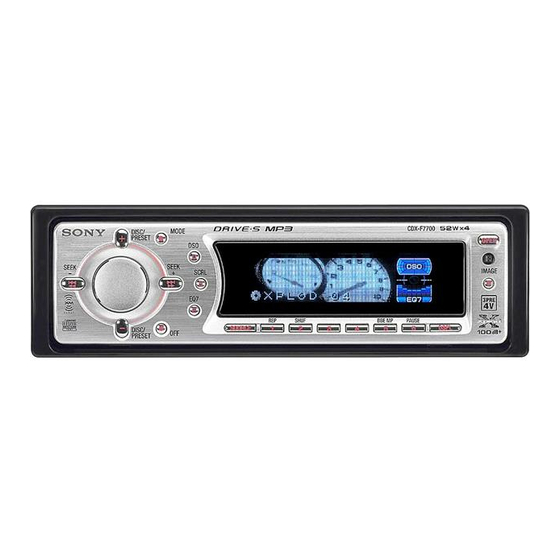
Photo: CDX-F7700
Model Name Using Similar Mechanism
CD Drive Mechanism Type
Optical Pick-up Name
SPECIFICATIONS
General
Outputs
Inputs
Tone controls
Loudness
Power requirements
Dimensions
Mounting dimensions
Mass
Supplied accessories
Design and specifications are subject to change without
notice.
FM/MW/LW COMPACT DISC PLAYER
AEP Model
UK Model
CDX-F7500/F7700
E Model
CDX-F7700/F7705X
MG-611MA-186//K
KSS1000E
Audio output terminals (front/rear)
Subwoofer output terminal (mono)
Power aerial relay control terminal
Power amplifier control terminal
Telephone ATT control terminal
Illumination control terminal
BUS control input terminal
BUS audio input or AUX IN terminal
Remote controller input terminal
Aerial input terminal
Bass ±8 dB at 100 Hz
Treble ±8 dB at 10 kHz
+8 dB at 100 Hz
+2 dB at 10 kHz
12 V DC car battery
(negative earth)
Approx. 178 × 50 × 178 mm (w/h/d)
Approx. 182 × 53 × 161 mm (w/h/d)
Approx. 1.3 kg
Parts for installation and connections (1 set)
Front panel case (1)
Card remote commander RM-X140
CDX-F7700
1
Advertisement
Table of Contents

Related Manuals for Sony CDX-F7500


Summary of Contents for Sony CDX-F7500
- Page 1 4 – 8 ohms Maximum power output CDX-F7700: 52 W × 4 (at 4 ohms) CDX-F7500: 50 W × 4 (at 4 ohms) FM/MW/LW COMPACT DISC PLAYER Sony Corporation 9-877-604-02 2004D04-1 e Vehicle Company © 2004. 04 Published by Sony Engineering Corporation...
- Page 2 COMPONENTS IDENTIFIED BY MARK 0 OR DOTTED LINE WITH MARK 0 ON THE SCHEMATIC DIAGRAMS AND IN THE PARTS LIST ARE CRITICAL TO SAFE OPERATION. REPLACE THESE COMPONENTS WITH SONY PARTS WHOSE PART NUMBERS APPEAR AS SHOWN IN THIS MANUAL OR IN SUPPLEMENTS PUBLISHED BY SONY.
- Page 3 CDX-F7500/F7700 Notes on CD-Rs (recordable CDs)/CD-RWs (rewritable UNLEADED SOLDER CDs) Boards requiring use of unleaded solder are printed with the lead This unit can play the following discs: free mark (LF) indicating the solder contains no lead. (Caution: Some printed circuit boards may not come printed with the lead free mark due to their particular size.)
-
Page 4: Table Of Contents
CDX-F7500/F7700 TABLE OF CONTENTS 1. GENERAL Location of Controls ..............5 Connections ................6 2. DISASSEMBLY 2-1. Sub Panel Assy (CD) ............9 2-2. CD Mechanism Block ............9 2-3. Main Board ............... 10 2-4. Chassis (T) Sub Assy ............10 2-5. -
Page 5: General
To store stations/receive stored stations. device is connected to AUX IN terminal of the unit. (With optional unit) MODE CD/MD: When you connect a Sony portable device and CD/ (1): REP 14 MD unit(s) at the same time, use the AUX IN Press selector. -
Page 6: Connections
CDX-F7500/F7700 Connections (AEP, UK Model) Auxiliary equipment such as portable DVD player Note for the aerial connecting Hinweis zum Anschließen der Antenne Nota per il collegamento dell’antenna (not supplied) If your car aerial is an ISO (International Wenn Ihre Fahrzeugantenne der ISO-Norm Se l’antenna dell’auto è... - Page 7 CDX-F7500/F7700 Connections (E Model)
-
Page 8: Disassembly
CDX-F7500/F7700 SECTION 2 DISASSEMBLY Note : This set can be disassemble according to the following sequence. 2-1. SUB PANEL ASSY (CD) (Page 9) 2-2. CD MECHANISM BLOCK (Page 9) 2-10. SERVO BOARD 2-3. MAIN BOARD 2-4. CHASSIS (T) SUB ASSY... -
Page 9: Sub Panel Assy (Cd)
CDX-F7500/F7700 Note : Follow the disassembly procedure in the numerical order given. 2-1. SUB PANEL ASSY (CD) 3 two claws 2 two claws CN601 1 two screws (+PTT 2.6 x 6) 5 sub panel assy (CD) 2-2. CD MECHANISM BLOCK... -
Page 10: Main Board
CDX-F7500/F7700 2-3. MAIN BOARD 6 cord 2 two screws (+PTT 2.6 x 8) 1 three ground point screws (+PTT 2.6 x 6) 5 screw (+PTT 2.6 x 8) 4 CN401 3 MAIN board 4 insulating sheet 2-4. CHASSIS (T) SUB ASSY... -
Page 11: Roller Arm Assy
CDX-F7500/F7700 2-5. ROLLER ARM ASSY 3 washer (1.1 – 2.5) 5 roller arm assy 4 worm wheel (RA) 2 spring (RAR) 1 spring (RAL) 2-6. CHASSIS (OP) ASSY qa chassis (OP) assy 0 compression spring (damper) lever (D) 4 washer... -
Page 12: Optical Pick-Up
CDX-F7500/F7700 2-7. OPTICAL PICK-UP 2 chucking arm sub assy 5 claw 1 tension coil spring (CHKG) 7 optical pick-up 6 main shaft 4 rack (SL) 3 screw (+B 1.4 x 5) 2-8. SL MOTOR ASSY (M902) 1 screw (+P 1.4 x 1.8) -
Page 13: Le Motor Assy (M903)
CDX-F7500/F7700 2-9. LE MOTOR ASSY (M903) 8 screw 0 worm (LEB) assy (+M 1.7 x 2.5) 9 bearing (LEB) 2 washer qa screw (+M 1.7 x 2.5) qf two toothed lock screws 3 gear (LE1) (+M 1.4 ) lever (D) -
Page 14: Diagrams
CDX-F7500/F7700 SECTION 3 DIAGRAMS 3-1. IC PIN DESCRIPTIONS • IC3 CXD3059BR (DIGITAL SERVO/DIGITAL SIGNAL PROCESSOR) (SERVO BOARD (1/2)) Pin No. Pin Name Pin Description MIRR Mirrer signal input/output DFCT Defect signal input/output Focus OK signal input/output — Ground pin LOCK Not used in this set. - Page 15 CDX-F7500/F7700 Pin No. Pin Name Pin Description CLTV VCO1 control voltage input FILO Filter signal output for master PLL FILI Filter signal input for master PLL Charge pomp output for master PLL AVDD5 — Analog power supply pin DDVROUT DC/DC converter output...
- Page 16 CDX-F7500/F7700 Pin No. Pin Name Pin Description XLAT Latch signal input CLOK Serial data transfer clock signal input — Digital power supply pin for internal SENS SENS signal output SCLK Clock signal input for SENS serial data read out ATSK...
- Page 17 Electronic volume mute signal output I2C CKO I2C bus serial clock output I2C SIO I2C bus serial data output UNI SO SONY bus serial data output UNI SI SONY bus serial data input UNI CKO SONY bus serial clock output TUNER ATT...
- Page 18 CDX-F7500/F7700 Pin No. Pin Name Pin Description CD LM EJECT CD eject signal output CD RESET CD reset signal output CD AO CD AO signal output CD STB CD strobe signal output (NCO) Not used CD RF OK CD RF OK signal input...
- Page 19 CDX-F7500/F7700 • IC901 M30823MH-080GP (DISPLAY CONTROL) (KEY BOARD) Pin No. Pin Name Pin Description SYS CE Main chip enable input (NCO) Not used FL DAT3 FL serial data output 3 (NCO) Not used FL CLK IN FL serial clock input BYTE Connecting to ground.
-
Page 20: Block Diagram -Cd Section
CDX-F7500/F7700 3-2. BLOCK DIAGRAM — CD SECTION — • R-ch is omitted due to same as L-ch. • Siganal Path : CD PLAY DETECTOR MAIN RFACO 42 RFACI ASYO 45 ASYI AOUT1 CD-L SECTION (Page 21) AOUT2 R-CH RF AMP,DIGITAL SERVO,... -
Page 21: Block Diagram -Main Section
CDX-F7500/F7700 3-3. BLOCK DIAGRAM — MAIN SECTION — F7500 F7700 IC470 CN401 SUB OUT(MONO) MUTE F7500 ELECTRONIC VOLUME Q470 GROUND SW IC401 Q408 PB LCH PB RCH R-CH AUDIO IN R-CH IC402 OUTSW CD-L 42 CD LCH SECTION R-CH 43 CD RCH... -
Page 22: Block Diagram -Display Section
CDX-F7500/F7700 3-4. BLOCK DIAGRAM — DISPLAY SECTION — SYSTEM CONTROL DISPLAY CONTROL IC303 (3/3) IC901 FL DAT1 ROTARY REIN0 ENCODER FL DAT2 DISP CE 1 CE ENC901(1/2) REIN1 FL DAT3 DISP SI DISP SO KEY MATRIX DISP CKO KEYIN0 FL CLK... -
Page 23: Note For Printed Wiring Boards And Schematic Diagrams
CDX-F7500/F7700 3-5. NOTE FOR PRINTED WIRING BOARDS AND SCHEMATIC DIAGRAMS 3-6. WAVEFORMS THIS NOTE IS COMMON FOR PRINTED WIRING BOARDS AND SCHEMATIC DIAGRAMS. — Main Board — — Servo Board — (MODE: CD PLAY) (In addition to this, the necessary note is printed in each block.) -
Page 24: Schematic Diagram –Cd Mechanism Section (1/2)
CDX-F7500/F7700 3-8. SCHEMATIC DIAGRAM — CD MECHANISM SECTION (1/2) — • Refer to page 23 for Waveforms. TP59 TP57 TP60 TP61 TP180 TP181 TP129 TP72 TP123 TP128 TP139 TP53 TP56 TP140 TP55 TP167 TP54 TP48 TP49 TP47 TP71 TP175 R114... -
Page 25: Schematic Diagram –Cd Mechanism Section (2/2)
CDX-F7500/F7700 • Refer to page 23 for Waveforms. 3-9. SCHEMATIC DIAGRAM — CD MECHANISM SECTION (2/2) — • Refer to page 36 for IC Block Diagram. (Page 24) R136 R146 R117 TP70 IC B/D TP11 TP12 R140 TP19 TP20 TP17... -
Page 26: Schematic Diagram -Main Section (1/3)
CDX-F7500/F7700 3-11. SCHEMATIC DIAGRAM — MAIN SECTION (1/3) — • Refer to page 36 for IC Block Diagram. C555 IC B/D C554 L501 R553 R478 C557 C556 R477 R473 R472 C470 TUX501 C475 IC550 R402 IC470 R552 FB442 C553 R550... -
Page 27: Schematic Diagram -Main Section (2/3)
CDX-F7500/F7700 3-12. SCHEMATIC DIAGRAM — MAIN SECTION (2/3) — • Refer to page 36 for IC Block Diagram. C215 C210 C205 IC B/D D111 D110 CNP101 D113 C206 R203 D112 C218 R205 CN103 CN102 C208 C216 D114 C209 C217 IC201... -
Page 28: Schematic Diagram -Main Section (3/3)
CDX-F7500/F7700 • Refer to page 23 for Waveforms. 3-13. SCHEMATIC DIAGRAM — MAIN SECTION (3/3) — • Refer to page 37 for IC Block Diagram. (Page 28) (Page 27) (Page D275 CNP301 FB329 D904 FB325 C336 L303 FB326 C335 C342... -
Page 29: Schematic Diagram -Sub Section
CDX-F7500/F7700 3-16. SCHEMATIC DIAGRAM — SUB SECTION — CNP501 (Page 35) (Page 28) D991 D990 R990 S901 R991 LED932 LED931... -
Page 30: Schematic Diagram -Key Section
CDX-F7500/F7700 3-18. SCHEMATIC DIAGRAM — KEY SECTION — ENC901(1/2) CN901 R979 R981 R918 R919 R920 R921 R922 R923 R924 R925 R926 R927 R983 R985 C901 R980 R984 LED923 LED901 LSW903(2/2) LSW905(2/2) LSW907(2/2) LSW901(2/2) LED924 D901 LSW902(2/2) LSW904(2/2) LSW906(2/2) LSW908(2/2) LED910... -
Page 31: Ic Block Diagrams
CDX-F7500/F7700 3-19. IC BLOCK DIAGRAMS IC7 R1114N151D-TR-FA IC401 TDA7416 (MAIN Board (1/3)) (SERVO Board (2/2)) IC1 LA6560-TE-L-E (SERVO Board (2/2)) 30 29 24 23 5 VOUT HIGH PASS MIXER FILTER2 36 S-GND THERMAL SHUTDOWN INPUT 35 VCONT SOFT STEP FADER... - Page 32 CDX-F7500/F7700 IC201 TDA8588AJ/N2 (MAIN Board (2/3)) OUT FL- I2C BUS OUT FL+ OUT RL- PGND3 OUT RL+ INRL INFL SGND PROTECTION DIAGNOSTIC INFR INRR AC GND OUT RR+ PGND2 OUT RR- OUT FR+ STANDBY MUTE OUT FR- CHIP DETECT PGND1...
-
Page 33: Exploded Views
CDX-F7500/F7700 SECTION 4 EXPLODED VIEWS NOTE: • The mechanical parts with no reference • Color Indication of Appearance Parts The components identified by mark 0 or dotted line with mark number in the exploded views are not supplied. Example : 0 are critical for safety. -
Page 34: Front Panel Section
CDX-F7500/F7700 4-2. FRONT PANEL SECTION FL900 not supplied (KEY board) not supplied not supplied not supplied Ref. No. Part No. Description Remark Ref. No. Part No. Description Remark X-3384-508-1 BUTTON KIT ASSY (S) X-3378-390-3 CASE ASSY (for FRONT PANEL) 3-265-937-01 SPRING (OPEN) -
Page 35: Cd Mechanism Section (1)
CDX-F7500/F7700 4-3. CD MECHANISM SECTION (1) (MG-611MA-186//K) not supplied not supplied (SENSOR board) not supplied not supplied Ref. No. Part No. Description Remark Ref. No. Part No. Description Remark A-3372-455-A CHASSIS (T) SUB ASSY 3-253-748-01 DAMPER (S) 3-253-729-01 SPRING (LTR), TENSION COIL 3-352-758-31 SCREW (M1.7), TOOTHED LOCK... -
Page 36: Cd Mechanism Section (2)
CDX-F7500/F7700 4-4. CD MECHANISM SECTION (2) (MG-611MA-186//K) (including M901) M902 not supplied not supplied not supplied The components identified by mark 0 or dotted line with mark. 0 are critical for safety. Replace only with part number specified. Ref. No. -
Page 37: Cd Mechanism Section (3)
CDX-F7500/F7700 4-5. CD MECHANISM SECTION (3) (MG-611MA-186//K) M903 Ref. No. Part No. Description Remark Ref. No. Part No. Description Remark 3-262-755-01 WASHER (1.1-2.5) 3-259-467-01 BRACKET (LEM) 3-259-024-01 WHEEL (RA), WORM 3-345-648-91 SCREW (M1.4), TOOTHED LOCK A-3337-633-A ARM ASSY, ROLLER A-3372-456-A WORM (LEB) ASSY... -
Page 38: Cd Mechanism Section (4)
CDX-F7500/F7700 4-6. CD MECHANISM SECTION (4) (MG-611MA-186//K) Ref. No. Part No. Description Remark Ref. No. Part No. Description Remark 3-259-429-01 WHEEL (LE), WORM 3-899-829-01 WASHER (SLIT) 3-344-223-01 WASHER 3-259-032-01 GEAR (LE2) 3-259-470-01 GEAR (LE1) A-3372-453-A CHASSIS (M) BLOCK ASSY 3-253-755-02 LEVER (D) -
Page 39: Electrical Parts List
CDX-F7500/F7700 SECTION 5 ELECTRICAL PARTS LIST NOTE: • Due to standardization, replacements in • Items marked “*” are not stocked since The components identified by mark 0 or dotted line with mark. the parts list may be different from the they are seldom required for routine service. - Page 40 CDX-F7500/F7700 Ref. No. Part No. Description Remark Ref. No. Part No. Description Remark LED914 6-500-204-01 LED CL-190UB2-X-T (DISC/PRESET +) R905 1-218-851-11 METAL CHIP 1.5K 0.5% 1/10W (F7700) R906 1-218-851-11 METAL CHIP 1.5K 0.5% 1/10W LED914 6-500-450-01 LED CL-195SR-CD-T (DISC/PRESET +)
- Page 41 CDX-F7500/F7700 MAIN Ref. No. Part No. Description Remark Ref. No. Part No. Description Remark R934 1-216-811-11 METAL CHIP 1/10W S904 1-771-884-31 SWITCH, TACTILE (SEEK –/./m) (F7700) S905 1-771-884-31 SWITCH, TACTILE (DISC/PRESET +) R934 1-216-820-11 METAL CHIP 1/10W S906 1-771-884-31 SWITCH, TACTILE (DISC/PRESET –)
- Page 42 CDX-F7500/F7700 MAIN Ref. No. Part No. Description Remark Ref. No. Part No. Description Remark C215 1-115-340-11 CERAMIC CHIP 0.22uF C400 1-124-721-11 ELECT 10uF C216 1-162-927-11 CERAMIC CHIP 100PF (F7700) C217 1-162-927-11 CERAMIC CHIP 100PF C401 1-126-947-11 ELECT 47uF C218 1-125-891-11 CERAMIC CHIP 0.47uF...
- Page 43 CDX-F7500/F7700 MAIN Ref. No. Part No. Description Remark Ref. No. Part No. Description Remark C452 1-164-156-11 CERAMIC CHIP 0.1uF D109 8-719-200-82 DIODE 11ES2 (F7700) D110 8-719-053-18 DIODE 1SR154-400TE-25 C453 1-164-156-11 CERAMIC CHIP 0.1uF D111 8-719-053-18 DIODE 1SR154-400TE-25 (F7700) D112 8-719-053-18 DIODE 1SR154-400TE-25...
- Page 44 CDX-F7500/F7700 Ver 1.1 MAIN Ref. No. Part No. Description Remark Ref. No. Part No. Description Remark IC252 8-759-679-05 IC TC7WH34FU(TE12R) Q452 6-550-752-01 TRANSISTOR DTC614TKT146 (F7700) IC271 6-705-373-01 IC MM3123DPLE Q453 6-550-752-01 TRANSISTOR DTC614TKT146 (F7700) IC273 8-759-679-05 IC TC7WH34FU(TE12R) Q470 6-550-752-01 TRANSISTOR DTC614TKT146...
- Page 45 CDX-F7500/F7700 MAIN Ref. No. Part No. Description Remark Ref. No. Part No. Description Remark R270 1-216-837-11 METAL CHIP 1/10W R402 1-216-813-11 METAL CHIP 1/10W R271 1-216-845-11 METAL CHIP 100K 1/10W (F7700) R272 1-216-295-11 SHORT CHIP 0 (F7500) R402 1-216-864-11 SHORT CHIP...
- Page 46 CDX-F7500/F7700 MAIN SENSOR SERVO Ref. No. Part No. Description Remark Ref. No. Part No. Description Remark R454 1-216-845-11 METAL CHIP 100K 1/10W R643 1-216-296-11 SHORT CHIP (F7700) R910 1-216-845-11 METAL CHIP 100K 1/10W R455 1-216-835-11 METAL CHIP 1/10W R920 1-216-073-00 RES-CHIP...
- Page 47 CDX-F7500/F7700 SERVO Ref. No. Part No. Description Remark Ref. No. Part No. Description Remark 1-162-962-11 CERAMIC CHIP 470PF < JUMPER RESISTOR > 1-162-967-11 CERAMIC CHIP 0.0033uF 10% 1-162-970-11 CERAMIC CHIP 0.01uF 1-216-864-11 SHORT CHIP 1-126-208-21 ELECT CHIP 47uF 1-216-864-11 SHORT CHIP 1-107-826-11 CERAMIC CHIP 0.1uF...
- Page 48 CDX-F7500/F7700 SERVO Ref. No. Part No. Description Remark Ref. No. Part No. Description Remark 1-218-957-11 RES-CHIP 2.2K 1/16W R128 1-218-965-11 RES-CHIP 1/16W 1-218-977-11 RES-CHIP 100K 1/16W R129 1-218-965-11 RES-CHIP 1/16W 1-218-941-81 RES-CHIP 1/16W R133 1-216-864-11 SHORT CHIP 1-218-953-11 RES-CHIP 1/16W...
- Page 49 CDX-F7500/F7700 Ref. No. Part No. Description Remark Ref. No. Part No. Description Remark MISCELLANEOUS PARTS FOR INSTALLATION AND CONNCTIONS *************** ************************************** 1-790-375-12 CORD (WITH CONNECTOR) (SUB OUT (MONO)) X-3382-647-1 FRAME ASSY, FITTING 1-776-527-71 CORD (WITH CONNECTOR) (ISO) (POWER) X-3366-405-1 SCREW ASSY (EXP), FITTING...
- Page 50 CDX-F7500/F7700 MEMO...
- Page 51 CDX-F7500/F7700 REVISION HISTORY Clicking the version allows you to jump to the revised page. Also, clicking the version at the upper on the revised page allows you to jump to the next revised page. Ver. Date Description of Revision 2004. 02 2004.
- Page 52 www.s-manuals.com...
Need help?
Do you have a question about the CDX-F7500 and is the answer not in the manual?
Questions and answers