Sony CDX-F7700 Service Manual
Fm/am compact disc player
Hide thumbs
Also See for CDX-F7700:
- Operating instructions manual (186 pages) ,
- Install manual (4 pages) ,
- Service manual (56 pages)
Table of Contents
Advertisement
CDX-F7700/F7705X
SERVICE MANUAL
Ver 1.0 2004. 01
• The tuner and CD sections have no adjustments.
AUDIO POWER SPECIFICATIONS (US Model)
POWER OUTPUT AND TOTAL HARMONIC DISTORTION
23.2 watts per channel minimum continuous average power into
4 ohms, 4 channels driven from 20 Hz to 20 kHz with no more
than 5% total harmonic distortion.
CD player section
Signal-to-noise ratio
120 dB
Frequency response
10 – 20,000 Hz
Wow and flutter
Below measurable limit
Tuner section
FM
Tuning range
87.5 – 107.9 MHz
Antenna terminal
External antenna connector
Intermediate frequency
10.7 MHz/450 kHz
Usable sensitivity
9 dBf
Selectivity
75 dB at 400 kHz
Signal-to-noise ratio
67 dB (stereo),
69 dB (mono)
Harmonic distortion at 1 kHz
0.5% (stereo),
0.3% (mono)
Separation
35 dB at 1 kHz
Frequency response
30 – 15,000 Hz
AM
Tuning range
530 – 1,710 kHz
Antenna terminal
External antenna connector
Intermediate frequency
10.7 MHz/450 kHz
Sensitivity
30 µV
Power amplifier section
Outputs
Speaker outputs
(sure seal connectors)
Speaker impedance
4 – 8 ohms
Maximum power output 52 W × 4 (at 4 ohms)
Sony Corporation
9-877-508-01
2004A04-1
e Vehicle Company
© 2004. 01
Published by Sony Engineering Corporation
Photo: CDX-F7700
Model Name Using Similar Mechanism
CD Drive Mechanism Type
Optical Pick-up Name
SPECIFICATIONS
General
Outputs
Inputs
Tone controls
Loudness
Power requirements
Dimensions
Mounting dimensions
Mass
Supplied accessories
Design and specifications are subject to change without
notice.
FM/AM COMPACT DISC PLAYER
US Model
Canadian Model
CDX-F5500
MG-611MA-186//K
KSS1000E
Audio output terminals (front/rear)
Subwoofer output terminal (mono)
Power antenna relay control terminal
Power amplifier control terminal
Telephone ATT control terminal
Illumination control terminal
BUS control input terminal
BUS audio input or AUX IN terminal
Remote controller input terminal
Antenna input terminal
Bass ±10 dB at 62 Hz
Treble ±10 dB at 16 kHz
+8 dB at 100 Hz
+2 dB at 10 kHz
12 V DC car battery
(negative ground)
Approx. 178 × 50 × 178 mm
× 2 × 7
(7
in.) (w/h/d)
1/8
1/8
Approx. 182 × 53 × 161 mm
(7
× 2
× 6
in.) (w/h/d)
1/4
1/8
3/8
Approx. 1.3 kg (2 lb. 14 oz.)
Parts for installation and connections (1 set)
Front panel case (1)
Card remote commander RM-X141A
1
Advertisement
Table of Contents

Related Manuals for Sony CDX-F7700


Summary of Contents for Sony CDX-F7700
- Page 1 Speaker outputs (sure seal connectors) Speaker impedance 4 – 8 ohms Maximum power output 52 W × 4 (at 4 ohms) FM/AM COMPACT DISC PLAYER Sony Corporation 9-877-508-01 2004A04-1 e Vehicle Company © 2004. 01 Published by Sony Engineering Corporation...
- Page 2 LES COMPOSANTS IDENTIFIÉS PAR UNE MARQUE 0 SUR LES DIAGRAMMES SCHÉMATIQUES ET LA LISTE DES PIÈCES SONT CRITIQUES POUR LA SÉCURITÉ DE FONCTIONNEMENT. NE REMPLACER CES COMPOSANTS QUE PAR DES PIÈCES SONY DONT LES NUMÉROS SONT DONNÉS DANS CE MANUEL OU DANS LES SUPPLÉMENTS PUBLIÉS PAR SONY.
- Page 3 CDX-F7700/F7705X Notes on CD-Rs (recordable CDs)/CD-RWs (rewritable UNLEADED SOLDER CDs) Boards requiring use of unleaded solder are printed with the lead This unit can play the following discs: free mark (LF) indicating the solder contains no lead. (Caution: Some printed circuit boards may not come printed with the lead free mark due to their particular size.)
-
Page 4: Table Of Contents
CDX-F7700/F7705X TABLE OF CONTENTS 1. GENERAL Location of Controls ..............5 Connections ................7 2. DISASSEMBLY 2-1. Sub Panel Assy (CD) ............9 2-2. CD Mechanism Block ............9 2-3. Main Board ............... 10 2-4. Chassis (T) Sub Assy ............10 2-5. -
Page 5: General
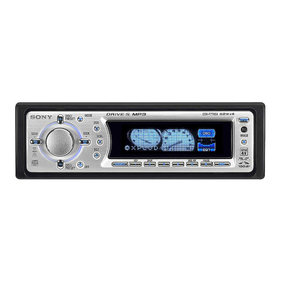
AUX IN terminal of the unit. (With optional unit) MODE (1): REP 14 When you connect a Sony portable device and CD/ (2): SHUF 15 MD unit(s) at the same time, use the AUX IN Press selector. - Page 6 CDX-F7700/F7705X DISC/ MODE PRESET OPEN SEEK SEEK – SCRL IMAGE SHUF BBE MP PAUSE SOURCE DSPL DISC/ PRESET CDX-F7705X/F7700 The buttons on the unit share the same functions as those on the card remote commander. a 5 SEEK/AMS (.m/M>) qd OFF (Stop/Power off) button*...
-
Page 7: Connections
CDX-F7700/F7705X Connections Source selector (not supplied) Sélecteur de source (non fourni) Supplied with the CD/MD changer Selector de fuente Fourni avec le changeur de CD/MD (no suministrado) Suministrado con el cambiador de CD/MD XA-C30 BUS AUDIO IN /AUX IN AUDIO OUT... -
Page 8: Disassembly
CDX-F7700/F7705X SECTION 2 DISASSEMBLY Note : This set can be disassemble according to the following sequence. 2-1. SUB PANEL ASSY (CD) (Page 9) 2-2. CD MECHANISM BLOCK (Page 9) 2-10. SERVO BOARD 2-3. MAIN BOARD 2-4. CHASSIS (T) SUB ASSY... -
Page 9: Sub Panel Assy (Cd)
CDX-F7700/F7705X Note : Follow the disassembly procedure in the numerical order given. 2-1. SUB PANEL ASSY (CD) 3 two claws 2 two claws CN601 1 two screws (+PTT 2.6 x 6) 5 sub panel assy (CD) 2-2. CD MECHANISM BLOCK... -
Page 10: Main Board
CDX-F7700/F7705X 2-3. MAIN BOARD 6 cord 2 two screws (+PTT 2.6 x 8) 1 three ground point screws (+PTT 2.6 x 6) 5 two screws (+PTT 2.6 x 8) 4 CN401 3 MAIN board 2-4. CHASSIS (T) SUB ASSY 4 claw 2 two screws (+P 1.7 x 2.2) -
Page 11: Roller Arm Assy
CDX-F7700/F7705X 2-5. ROLLER ARM ASSY 3 washer (1.1 – 2.5) 5 roller arm assy 4 worm wheel (RA) 2 spring (RAR) 1 spring (RAL) 2-6. CHASSIS (OP) ASSY qa chassis (OP) assy 0 compression spring (damper) lever (D) 4 washer... -
Page 12: Optical Pick-Up
CDX-F7700/F7705X 2-7. OPTICAL PICK-UP 2 chucking arm sub assy 5 claw 1 tension coil spring (CHKG) 7 optical pick-up 6 main shaft 4 rack (SL) 3 screw (+B 1.4 x 5) 2-8. SL MOTOR ASSY (M902) 1 screw (+P 1.4 x 1.8) -
Page 13: Le Motor Assy (M903)
CDX-F7700/F7705X 2-9. LE MOTOR ASSY (M903) 8 screw 0 woam (LEB) assy (+M 1.7 x 2.5) 9 bearing (LEB) 2 washer qa screw (+M 1.7 x 2.5) qf two toothed lock screws 3 gear (LE1) (+M 1.4 ) lever (D) -
Page 14: Diagrams
CDX-F7700/F7705X SECTION 3 DIAGRAMS 3-1. IC PIN DESCRIPTIONS • IC3 CXD3059AR (DIGITAL SERVO/DIGITAL SIGNAL PROCESSOR) (SERVO BOARD (1/2)) Pin No. Pin Name Pin Description MIRR Mirrer signal input/output DFCT Defect signal input/output Focus OK signal input/output — Ground pin LOCK Not used in this set. - Page 15 CDX-F7700/F7705X Pin No. Pin Name Pin Description CLTV VCO1 control voltage input FILO Filter signal output for master PLL FILI Filter signal input for master PLL Charge pomp output for master PLL AVDD5 — Analog power supply pin DDVROUT DC/DC converter output...
- Page 16 CDX-F7700/F7705X Pin No. Pin Name Pin Description XLAT Latch signal input CLOK Serial data transfer clock signal input — Digital power supply pin for internal SENS SENS signal output SCLK Clock signal input for SENS serial data read out ATSK...
- Page 17 Electronic volume mute signal output I2C CKO I2C bus serial clock output I2C SIO I2C bus serial data output UNI SO SONY bus serial data output UNI SI SONY bus serial data input UNI CKO SONY bus serial clock output TUNER ATT...
- Page 18 CDX-F7700/F7705X Pin No. Pin Name Pin Description CD LM EJECT CD eject signal output CD RESET CD reset signal output CD AO CD AO signal output CD STB CD strobe signal output (NCO) Not used CD RF OK CD RF OK signal input...
- Page 19 CDX-F7700/F7705X • IC901 M30823MH-080GP (DISPLAY CONTROL) (KEY BOARD) Pin No. Pin Name Pin Description SYS CE Main chip enable input (NCO) Not used FL DAT3 FL serial data output 3 (NCO) Not used FL CLK IN FL serial clock input BYTE Connecting to ground.
-
Page 20: Block Diagram -Cd Section
CDX-F7700/F7705X 3-2. BLOCK DIAGRAM — CD SECTION — • R-ch is omitted due to same as L-ch. • Siganal Path : CD PLAY DETECTOR MAIN RFACO 42 RFACI ASYO 45 ASYI AOUT1 CD-L SECTION (Page 21) AOUT2 R-CH RF AMP,DIGITAL SERVO,... -
Page 21: Block Diagram -Main Section
CDX-F7700/F7705X 3-3. BLOCK DIAGRAM — MAIN SECTION — IC470 CN401 SUB OUT(MONO) MUTE ELECTRONIC VOLUME GROUND SW Q470 IC401 Q408 PB LCH PB RCH R-CH AUDIO IN IC402 R-CH OUTSW (Page 20) CD-L 42 CD LCH SECTION R-CH 43 CD RCH... -
Page 22: Block Diagram -Display Section
CDX-F7700/F7705X 3-4. BLOCK DIAGRAM — DISPLAY SECTION — SYSTEM CONTROL DISPLAY CONTROL IC303 (3/3) IC901 FL DAT1 ROTARY REIN0 ENCODER FL DAT2 DISP CE 1 CE ENC901(1/2) REIN1 FL DAT3 DISP SI DISP SO KEY MATRIX DISP CKO KEYIN0 FL CLK... -
Page 23: Note For Printed Wiring Boards And Schematic Diagrams
CDX-F7700/F7705X 3-5. NOTE FOR PRINTED WIRING BOARDS AND SCHEMATIC DIAGRAMS 3-6. WAVEFORMS THIS NOTE IS COMMON FOR PRINTED WIRING BOARDS AND SCHEMATIC DIAGRAMS. — Main Board — — Servo Board — (MODE: CD PLAY) (In addition to this, the necessary note is printed in each block.) -
Page 24: Schematic Diagram -Cd Mechanism Section (1/2)
CDX-F7700/F7705X 3-8. SCHEMATIC DIAGRAM — CD MECHANISM SECTION (1/2) — • Refer to page 23 for Waveforms. TP59 TP57 TP60 TP61 TP180 TP181 TP129 TP72 TP123 TP128 TP139 TP53 TP56 TP140 TP55 TP54 TP167 TP48 TP49 TP71 TP175 TP47 R114... -
Page 25: Schematic Diagram -Cd Mechanism Section (2/2)
CDX-F7700/F7705X • Refer to page 23 for Waveforms. 3-9. SCHEMATIC DIAGRAM — CD MECHANISM SECTION (2/2) — • Refer to page 36 for IC Block Diagram. (Page 24) R136 R146 R117 TP70 IC B/D TP11 TP12 R140 TP19 TP20 TP17... -
Page 26: Printed Wiring Boards -Cd Mechanism Section
CDX-F7700/F7705X 3-10. PRINTED WIRING BOARDS — CD MECHANISM SECTION — • Refer to page 23 for Circuit Boards Location. : Uses unleaded solder. R107 R139 R116 C110 R109 C109 R102 C115 R111 R144 R122 R128 R127 R143 R141 R119 R117... -
Page 27: Schematic Diagram -Main Section (1/3)
CDX-F7700/F7705X 3-11. SCHEMATIC DIAGRAM — MAIN SECTION (1/3) — • Refer to page 36 for IC Block Diagram. R477 R473 R472 C470 TUX501 C475 IC470 FB442 CN401 C442 C508 R402 C443 FB441 Q470 R407 R471 C509 J601 R432 R430 C507... -
Page 28: Schematic Diagram -Main Section (2/3)
CDX-F7700/F7705X 3-12. SCHEMATIC DIAGRAM — MAIN SECTION (2/3) — • Refer to page 36 for IC Block Diagram. C215 C210 C205 IC B/D D111 D110 D113 CNP101 C206 R203 D112 C218 R205 CN103 CN102 C208 C216 D114 C209 C217 IC201... -
Page 29: Schematic Diagram -Main Section (3/3)
CDX-F7700/F7705X • Refer to page 23 for Waveforms. 3-13. SCHEMATIC DIAGRAM — MAIN SECTION (3/3) — • Refer to page 37 for IC Block Diagram. (Page 28) (Page 27) (Page D275 CNP301 FB329 L303 FB325 C336 D904 FB326 C335 R240... -
Page 30: Printed Wiring Boards -Main Section
CDX-F7700/F7705X 3-14. PRINTED WIRING BOARDS — MAIN SECTION — • Refer to page 23 for Circuit Boards Location. : Uses unleaded solder. • Semiconductor Location Ref. No. Location D101 D104 D105 D106 D111 D271 Q271 Q171 Q281 Q181 Q470 C209... - Page 31 CDX-F7700/F7705X PJ401 CNJ101 J601 CNP102 D122 C199 D110 CNP101 C242 C211 F901 C205 C210 C288 C215 D112 IC201 R274 R410 R242 R185 R175 CN103 D102 R142 D103 R143 R243 R184 R284 R174 R275 CN102 D117 C101 D121 D114 D116 C225...
-
Page 32: Printed Wiring Board -Sub Section
CDX-F7700/F7705X 3-15. PRINTED WIRING BOARD — SUB SECTION — • Refer to page 23 for Circuit Boards Location. : Uses unleaded solder. (Page 34) D991 CNP501 LED932 R991 R990 LED931 D990 S901 (Page 31) -
Page 33: Schematic Diagram -Sub Section
CDX-F7700/F7705X 3-16. SCHEMATIC DIAGRAM — SUB SECTION — CNP501 (Page 35) (Page 28) D991 D990 R990 S901 R991 LED932 LED931... -
Page 34: Printed Wiring Board -Key Section
CDX-F7700/F7705X 3-17. PRINTED WIRING BOARD — KEY SECTION — • Refer to page 23 for Circuit Boards Location. : Uses unleaded solder. LED923 S905 S907 LED919 LED920 IC903 S908 D915 S912 LED915 LED913 LED911 S904 LED901 S909 S903 LED922 LED921... -
Page 35: Schematic Diagram -Key Section
CDX-F7700/F7705X 3-18. SCHEMATIC DIAGRAM — KEY SECTION — ENC901(1/2) CN901 R979 R980 R981 R918 R919 R920 R921 R922 R923 R924 R925 R926 R927 R983 R984 R985 C901 LED923 LED901 LED924 LSW903(2/2) LSW905(2/2) LSW907(2/2) LSW901(2/2) LED910 D901 LSW902(2/2) LSW904(2/2) LSW906(2/2) LSW908(2/2) -
Page 36: Ic Block Diagrams
CDX-F7700/F7705X 3-19. IC BLOCK DIAGRAMS IC7 R1114N151D-TR-FA IC401 TDA7416 (MAIN Board (1/3)) (SERVO Board (2/2)) IC1 LA6560-TE-L-E (SERVO Board (2/2)) 30 29 24 23 5 VOUT HIGH PASS MIXER FILTER2 36 S-GND THERMAL SHUTDOWN INPUT 35 VCONT SOFT STEP FADER... - Page 37 CDX-F7700/F7705X IC201 TDA8588AJ/N2 (MAIN Board (2/3)) OUT FL- I2C BUS OUT FL+ OUT RL- PGND3 OUT RL+ INRL INFL SGND PROTECTION DIAGNOSTIC INFR INRR AC GND OUT RR+ PGND2 OUT RR- OUT FR+ STANDBY MUTE OUT FR- CHIP DETECT DIAGNOSTIC...
-
Page 38: Exploded Views
CDX-F7700/F7705X SECTION 4 EXPLODED VIEWS NOTE: • The mechanical parts with no reference • Color Indication of Appearance Parts The components identified by mark 0 or dotted line with mark number in the exploded views are not supplied. Example : 0 are critical for safety. -
Page 39: Front Panel Section
CDX-F7700/F7705X 4-2. FRONT PANEL SECTION FL900 not supplied (KEY board) not supplied not supplied not supplied Ref. No. Part No. Description Remark Ref. No. Part No. Description Remark X-3384-492-1 BUTTON KIT ASSY (S) X-3384-495-1 PANEL ASSY, FRONT BACK 3-032-321-01 SPRING (OPEN) -
Page 40: Cd Mechanism Section (1)
CDX-F7700/F7705X 4-3. CD MECHANISM SECTION (1) (MG-611MA-186//K) not supplied not supplied (SENSOR board) not supplied not supplied Ref. No. Part No. Description Remark Ref. No. Part No. Description Remark A-3372-455-A CHASSIS (T) SUB ASSY 3-253-748-01 DAMPER (S) 3-253-729-01 SPRING (LTR), TENSION COIL 3-352-758-31 SCREW (M1.7), TOOTHED LOCK... -
Page 41: Cd Mechanism Section (2)
CDX-F7700/F7705X 4-4. CD MECHANISM SECTION (2) (MG-611MA-186//K) (including M901) M902 not supplied not supplied not supplied not supplied The components identified by Les composants identifiés par une mark 0 or dotted line with mark marque 0 sont critiques pour 0 are critical for safety. -
Page 42: Cd Mechanism Section (3)
CDX-F7700/F7705X 4-5. CD MECHANISM SECTION (3) (MG-611MA-186//K) M903 Ref. No. Part No. Description Remark Ref. No. Part No. Description Remark 3-262-755-01 WASHER (1.1-2.5) 3-259-467-01 BRACKET (LEM) 3-259-024-01 WHEEL (RA), WORM 3-345-648-91 SCREW (M1.4), TOOTHED LOCK A-3337-633-A ARM ASSY, ROLLER A-3372-456-A WORM (LEB) ASSY... -
Page 43: Cd Mechanism Section (4)
CDX-F7700/F7705X 4-6. CD MECHANISM SECTION (4) (MG-611MA-186//K) Ref. No. Part No. Description Remark Ref. No. Part No. Description Remark 3-259-429-01 WHEEL (LE), WORM 3-899-829-01 WASHER (SLIT) 3-344-223-01 WASHER 3-259-032-01 GEAR (LE2) 3-259-470-01 GEAR (LE1) A-3372-453-A CHASSIS (M) BLOCK ASSY 3-253-755-01 LEVER (D) -
Page 44: Electrical Parts List
CDX-F7700/F7705X SECTION 5 ELECTRICAL PARTS LIST NOTE: • Due to standardization, replacements in • Items marked “*” are not stocked since The components identified by mark 0 or dotted line with mark the parts list may be different from the they are seldom required for routine service. - Page 45 CDX-F7700/F7705X Ref. No. Part No. Description Remark Ref. No. Part No. Description Remark LED913 6-500-204-01 LED CL-190UB2-X-T (SEEK +/>/M) < RESISTOR > (F7705X) LED913 6-500-450-01 LED CL-195SR-CD-T (SEEK +/>/M) R901 1-219-286-11 RES-CHIP 1/16W (F7700) R902 1-219-286-11 RES-CHIP 1/16W LED914 6-500-204-01 LED CL-190UB2-X-T (DISC/PRESET +)
- Page 46 CDX-F7700/F7705X MAIN Ref. No. Part No. Description Remark Ref. No. Part No. Description Remark R932 1-216-811-11 METAL CHIP 1/10W R985 1-216-821-11 METAL CHIP 1/10W (F7705X) (F7700) R932 1-216-820-11 METAL CHIP 1/10W R987 1-216-845-11 METAL CHIP 100K 1/10W (F7700) R933 1-216-820-11 METAL CHIP 1/10W <...
- Page 47 CDX-F7700/F7705X MAIN Ref. No. Part No. Description Remark Ref. No. Part No. Description Remark C219 1-125-891-11 CERAMIC CHIP 0.47uF C430 1-162-965-11 CERAMIC CHIP 0.0015uF 10% C221 1-126-933-11 ELECT 100uF C431 1-162-927-11 CERAMIC CHIP 100PF C223 1-126-964-11 ELECT 10uF C432 1-136-154-00 FILM 0.012uF...
- Page 48 CDX-F7700/F7705X MAIN Ref. No. Part No. Description Remark Ref. No. Part No. Description Remark < DIODE > FB329 1-216-295-11 SHORT CHIP FB330 1-216-295-11 SHORT CHIP D101 8-719-083-66 DIODE UDZS-TE17-18B FB441 1-414-813-11 FERRITE, EMI (SMD) D102 8-719-083-66 DIODE UDZS-TE17-18B FB442 1-414-813-11 FERRITE, EMI (SMD)
- Page 49 CDX-F7700/F7705X MAIN Ref. No. Part No. Description Remark Ref. No. Part No. Description Remark Q408 8-729-053-84 FET SSM3KO9FU(T5LSONY1) R275 1-216-841-11 METAL CHIP 1/10W Q450 6-550-752-01 TRANSISTOR DTC614TKT146 R284 1-216-813-11 METAL CHIP 1/10W Q451 6-550-752-01 TRANSISTOR DTC614TKT146 R285 1-216-841-11 METAL CHIP...
- Page 50 CDX-F7700/F7705X MAIN SENSOR SERVO Ref. No. Part No. Description Remark Ref. No. Part No. Description Remark R427 1-216-864-11 METAL CHIP 1/10W R642 1-216-296-11 SHORT CHIP R429 1-216-086-00 RES-CHIP 1/10W R643 1-216-296-11 SHORT CHIP R430 1-216-082-00 RES-CHIP 1/10W R910 1-216-845-11 METAL CHIP...
- Page 51 CDX-F7700/F7705X SERVO Ref. No. Part No. Description Remark Ref. No. Part No. Description Remark 1-162-962-11 CERAMIC CHIP 470PF < JUMPER RESISTOR > 1-162-967-11 CERAMIC CHIP 0.0033uF 10% 1-162-970-11 CERAMIC CHIP 0.01uF 1-216-864-11 METAL CHIP 1/10W 1-126-208-21 ELECT CHIP 47uF 1-216-864-11 METAL CHIP...
- Page 52 CDX-F7700/F7705X SERVO Ref. No. Part No. Description Remark Ref. No. Part No. Description Remark 1-218-957-11 RES-CHIP 2.2K 1/16W R128 1-218-965-11 RES-CHIP 1/16W 1-218-977-11 RES-CHIP 100K 1/16W R129 1-218-965-11 RES-CHIP 1/16W 1-218-941-81 RES-CHIP 1/16W R133 1-216-864-11 METAL CHIP 1/10W 1-218-953-11 RES-CHIP...
- Page 53 CDX-F7700/F7705X Ref. No. Part No. Description Remark MISCELLANEOUS *************** 1-776-207-72 CORD (WITH CONNECTOR) (POWER) 1-790-375-12 CORD (WITH CONNECTOR) (SUB OUT (MONO)) 0 153 8-820-207-02 OPTICAL PICK-UP (KSS1000E/K1RP) A-3337-640-A CHASSIS (OP) SUB ASSY (including M901) F901 1-532-877-11 FUSE (BLADE TYPE) (AUTO FUSE) 10A...
- Page 54 CDX-F7700/F7705X REVISION HISTORY Clicking the version allows you to jump to the revised page. Also, clicking the version at the upper on the revised page allows you to jump to the next revised page. Ver. Date Description of Revision 2004. 01...
Need help?
Do you have a question about the CDX-F7700 and is the answer not in the manual?
Questions and answers