Table of Contents
Advertisement
Advertisement
Table of Contents

Related Manuals for Toshiba MM20E45


Summary of Contents for Toshiba MM20E45
-
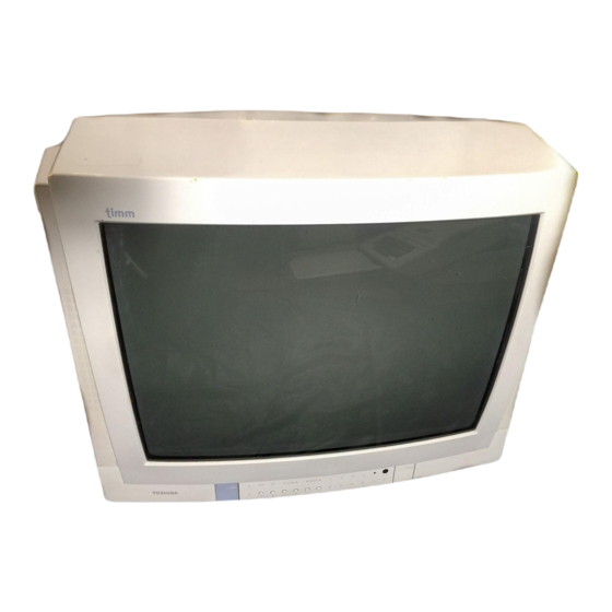
Page 1: Colour Television
FILE NO.016-9502 TECHNICAL TRAINING MANUAL COLOUR TELEVISION N5MM1 Chassis... -
Page 2: Table Of Contents
CONTENTS SECTION I OUTLINE SECTION II CHANNEL SELECTION CIRCUIT SECTION III RGB SIGNAL PROCESSING CIRCUIT SECTION IV CRT DRIVE CIRCUIT SECTION V MODE DISCRIMINATING CIRCUIT AND SYNC SIGNAL PROCESSING CIRCUIT SECTION VI SYNC SEPARATION CIRCUIT OF TV MODE SECTION VII HORIZONTAL AND VERTICAL OSCILLATION CIRCUIT SECTION VIII VERTICAL DEFLECTION CIRCUIT... - Page 3 SECTION I OUTLINE 1. OUTLINE OF N5MM1 CHASSIS 2. PC BOARD CONFIGURATION (MM20E45) (1) Power/V.C.D. PB5226 PB5226-1 Power This model is a 20” color TV with 181 channel tuner and built PB5226-2 V.C.D. in VGA and Mac II capability. The hybrid design of this model allows it to serve several purposes.
- Page 4 3. CONSTRUCTION OF CHASSIS...
- Page 5 4. LOCATION OF CONTROLS 4-1 TV Set...
- Page 6 4-2 Remote Control This Remote Control allows you to control the functions of your TV set from 16 feet (5m) away. The “*” marked function buttons do not have duplicate locations on your TV set. They can be controlled only by the Remote Control. Aim at the TV set...
- Page 7 4-3 Monitor Panel This TV set is equipped with RGB INPUT connector, RGB AUDIO INPUT jacks, S-VIDEO INPUT jack, VIDEO/AUDIO INPUT jacks and VARIABLE AUDIO OUTPUT jacks of connecting your desired personal computer and video/audio equipment. RGB INPUT Connector – provide for direct connection of a personal computer. RGB AUDIO INPUT Jacks –...
- Page 8 5. MM20E45 BLOCK DIAGRAM...
- Page 9 6. SPECIFICATIONS MODEL No. MM20E45 SPECIFICATIONS 1 Picture Tube D/T Invar 2 Channel Capacity 181ch 3 C. Caption 4 MTS with dbx 5 Bass, Treble, Balance GENERAL 6 Sub Audio Program 7 Remote hand unit Regu. 8 Nbr of RMT Button...
- Page 10 MM20E45 PC BOARD CONSTRUCTION ITEM MM20E45 NEW MODEL CIRCUIT NOTE 249 x 330 Def. Printed wiring board PB5227 part code (249.0 x 330.0) P/P-M/P: 23534680B Hole draw- Hole drawing: New ing: New PB5227 249 x 330 Power/Audio Printed wiring board...
-
Page 11: Channel Selection Circuit
8 bit microcomputer, TLCS-870 series for TV receivers, distortion, etc. TMP87CM34N (42 pins, built-in CCD) developed by Toshiba is employed. With this microcomputer each IC and circuit 2-1-4 Audio System Process IC shown below are controlled. - Page 12 3. SYSTEM BLOCK DIAGRAM...
- Page 13 3-1 Microcomputer Terminal Name and Operation Logic Terminal No. Terminal name I/O control resistor RELAY Positive logic MUTE Positive logic T BUS PERIOD T BUS CLOCK DATA T BUS DATA I-CSTOP Negative logic EXTA TV: H VIDEO/RGB: L SPKOFF Negative logic LINE21 KEY1 Local key input 0~5V...
- Page 14 3-2 DAC Terminal Name and Operation Logic (1) DAC (QX01) Terminal No. Terminal name Function Logic INTERFACE POWER SUPPLY T-BUS DATA INPUT TERMINAL T-BUS CLOCK INPUT TERMINAL T-BUS PERIOD INPUT TERMINAL RESET SUB-ADDRESS CHANGEOVER TERMINAL RGB CONT RGB CONTRAST 0~5V SUB BASS SYSTEM ON: L OFF: H (H at SPK OFF)
- Page 15 3-3 Remote Control Code Assignment Custom codes are 40H. Data Data Function Conti- Conti- Function code code nuity nuity EXIT SET UP OPTION RESET AUDIO RGB/TV/VIDEO MUTE K109 K110 POWER K111 K112 OPTION TIMER SET UP CH RTN CONTROL UP VOL UP CH UP RECALL...
- Page 16 3-4 Local Key Assignment 1. Detection method of Local Key Detection method of Local Key in N4ES chassis is analogue way to detect what voltage appears at local key input terminals (pins 13, 14) of Micom when the key is pressed. By this method, key detections of a maximum of 7 keys can be done, using local key input terminal (pin 13).
- Page 17 4. I C BUS INTERFACE OPERATION TIMING As an example of I C Bus interface operation timings, control for a memory IC will be shown below. 4-1 Write Mode (1 Byte) Fig. 2-1 4-2 Read Mode Fig. 2-1...
- Page 18 4-2-1 Generation of Start/stop Status Fig. 2-3 4-3 I C Bus Data Format (1) Memory IC * Write mode A0H (WRITE) * Read mode (2) DPC IC...
- Page 19 (3) U/V tuner unit Main screen tuner: COH FM: Variable divider control byte FL: Variable divider control byte CO: Charge pump sensitivity switching bit and test mode bit BA: Band switching bit...
- Page 20 5. SERVICE ADJUSTMENT MODE 1. Entering to Service Adjustment mode Press MUTE key on the remote control unit once. Press again the MUTE key, and keep pressing it. Keep pressing the MUTE key, press MUTE key on TV set. Address, Data 120H 8DH 120H 8DH Mode display of RGB...
- Page 21 ADDRESS OF SERVICE MODE a) Video section sub-adjustment b) OSD horizontal starting position Address Adjustment contents Address Adjustment contents 161H SUB BRIGHT 1E2H OSD-H.POSI 107H SUB COLOR 163H SUB TINT 108H SUB CONTRAST d) Multi-sound adjustment c) Deflection section sub-adjustment Address Adjustment contents Address...
-
Page 22: Rgb Signal Processing Circuit
SECTION III RGB SIGNAL PROCESSING CIRCUIT 1. OUTLINE (3) In TV reception, R-Y, G-Y and B-Y outputs of IC501 TA8801AN are selected by IC216 AN5862K and ICR03 The signal flow is explained as follows. RGB signal is input AN5862K, and are output at pins 5, 6, 8 of ICR03 to D-SUB 15P and is processed to be output at CRT Drive AN5862K. -
Page 23: Crt Drive Circuit
SECTION IV CRT DRIVE CIRCUIT 1. OUTLINE 2. CIRCUIT OPERATION CRT Drive circuit is designed with its output load resistance For example, Green axis circuit is explained as follows. decreased, to obtain wide frequency band, and heat-sink of (1) G signal which is output at pin 6 of AN5862K, is output transistor is enlarged in size. - Page 24 SECTION V MODE DISCRIMINATION CIRCUIT AND SYNC SIGNAL PROCESSING CIRCUIT Mode discriminating circuit performs to discriminate the kind of signals ; the signal which is input to D-SUB connector, is VGA, or is Macintosh signal. Sync signal processing circuit performs to process sync signals into shape which can be utilized in horizontal and vertical osc circuits, because the signals which are input to D-SUB connector from a personal computer have various figures.
- Page 25 2. OUTLINE OF SYNC SIGNAL PROCESSING CIRCUIT As mentioned above, signal input at D-SUB connector from personal computer, sometimes shows various shape of sync signal. Representative signals are described in Table-2. Kind Resolution Hor. Sync polarity Ver. Sync polarity IBM PGC 640 x 480 30.5kHz 60Hz...
- Page 26 3. MODE DISCRIMINATING CIRCUIT OPERATION The circuit which discriminates three modes of VGA, is as follows. ICH02 TC4028BP Fig. 2 Mode discrimination of VGA is done by the circuit in Fig. 2. ICH01 M52346SP also performs process of sync signal, and the logic output is shown in Table-3.
- Page 27 The outputs of VGA three modes are tabled as in Table-5. ICH01 M52346SP ICH02 TC4028BP Kind pin 11 pin 12 pin 13 pin 10 output pin 6 pin 8 pin 18 pin 19 (High) VGA480 Nega Nega pin 4 VGA400 Nega Posi pin 6...
- Page 28 Block diagram of ICH04 IR9331 is shown in Fig. 4. Fig. 4 Operation of F/V converter circuit using this IC are as follows. When horizontal sync signal is input to pin 6 of IC through QH03, this performs as a trigger, charge of capacitor CH13 which is connected to pin 5 begins.
- Page 29 In this period, current is supplied to capacitor CH14. This DH04, RH22 and RH23 perform to limit F/V convert voltage current is a constant current which is made in CURRENT so that it does not rise extremely, even though the higher MIRROR circuit, and is set with resistor RH18 connected to frequency than responsive range of this model, is input.
- Page 30 4. SYNC SIGNAL PROCESSING CIRCUIT This circuit also employs ICH01, the same as Mode discriminating circuit. Fig. 7 Sync signals are input as follows; TTL level hor sync or composite sync to pin 6, TTL level ver sync to pin 8, and Sync On Green sync to pin 4.
- Page 31 5. INTERFACE OF MODE DISCRIMINATING CIRCUIT AND CH. SELECTION MICOM The result of mode ident. explained in Section 3 is converted to d.c. and is supplied to pin 15 of Ch. Selection Micom ICA01. Fig. 8 Micom ICA01 recognizes kind of input signal by the voltage When frequency of input signal is lower than 28kHz, micom at pin 15, reads out data which are stored in memory and switches over automatically the size and display position of...
-
Page 32: Sync Separation Circuit Of Tv Mode
SECTION VI SYNC SEPARATION CIRCUIT OF TV MODE Sync separation of TV mode is done by the circuit contained in V/C/D IC the same as ordinary TV. This output signal and sync signal from RGB input, are switched in latter stage and are applied to hor and ver osc circuit. Operation of sync separation of V/C/D IC is as follow, though the switching circuit is explained later. - Page 33 2. THEORY OF OPERATION 2-1 H, V Sync Separation Circuits Fig. 2 shows a basic sync separation circuit and Fig.3 shows a composite video signal. When a composite video signal is applied Fig. 2: (1) The transistor is forward-biased with a voltage charged Fig.
-
Page 34: Horizontal And Vertical Oscillation Circuit
SECTION VII HORIZONTAL AND VERTICAL OSCILLATION CIRCUIT Ordinary TV uses the osc circuit contained inside V/C/D IC, but this model can not use this due to Multi Scan TV covering 15kHz to 40kHz. Other IC ICH08 (LA7860) for oscillation is added. This IC is for CRT monitor, and the hor osc frequency, the hor phase and the duty ratio of hor output pulse can be controlled by d.c. - Page 35 1. SECTIONAL EXPLANATION OF IC (1) Pin 1 is input terminal of hor sync signal. (3) Pin 3 is control terminal of H. SHIFT. Coupling capacitor of 0.01 µF is used to feed hor sync signal Range of control voltage is 0 to 2.5V. When control voltage of approx.
- Page 36 (5) Pin 5 is terminal of SHIFT GAIN CONTROL. (6) Time constant of pin 6 decides the phase shift controlled Range of control voltage is 0 to 2.5V. When control voltage by pin 5. is 2.5V, phase of FBP become most delayed condition to hor sync signal.
- Page 37 Ts is decided by the external time constant at pin 4, and is the (8) Pin 8 is control terminal of hor osc frequency of pin 11. first delay value controlled by d.c. voltage of pin 3. This The range of control voltage is 0 to 2.5V. When this voltage phase value is not independent of hor period.
- Page 38 (11) Pin 11 is to be connected with hor osc capacitor. (15) Pin 15 is control terminal of H. OUT DUTY. When shifting control range of frequency to upper or lower, Controlling the voltage at this terminal from 9V to approx. the value of capacitor is changed as requested.
- Page 39 (19) Pin 19 is H.LOCK output terminal. (22) Pin 22 This model does not use this terminal. This terminal gives Capacitor for producing AFC comparing wave is connected. output of discriminating result of approx. 5V, when hor sync The external capacitor is selected so that triangle waveform signal input from outside of IC and hor output at pin16 are in at pin22 becomes approx.
- Page 40 (25) Pin 25 is a terminal for ver blanking output. (27) Pin 27 is a terminal which is connected with capacitor The output voltage is approx. 5V when the terminal is set in which produces RAMP wave output at pins 25 and 26. high impedance.
- Page 41 (28) Pin 28 is a terminal which produces reference current of (30) Pin 30 is an input terminal of ver sync signal. ver osc circuit and RAMP wave making circuit. Ver sync signal of approx. 2V(p-p) is applied through The recommended value is 330k ohm. coupling capacitor 1µF.
- Page 42 2. CIRCUMFERENCE CIRCUIT OF IC The circuit which is consisted of QK13, CK25 and RK50, 2-1 Sync Signal Switching Circuit operates to eliminate sync pulse only for period of ver sync, The circuit switches the sync signal from V/C/D IC (IC501) so that in RGB mode top edge of picture does not show AFC in reception of TV or Video, and the sync signal from sync bending affected by ver sync, when composite sync is input.
- Page 43 2-2 Hor OSC frequency Control Circuit ICH13 the same as above sync signal is used for switching. To synchronizing hor deflection circuit to input signal, the The signal to switch the IC is sent though QH17. (See Fig. 29) circuit controls free-running frequency of hor osc circuit When the mode is selected with remote unit or key of TV set, responding with input signal.
- Page 44 Fig. 32 2-4 Other Circumference Circuit QH15 changes the duty ratio of hor output pulse (that is; hor drive pulse) of ICH08 so that the base current of hor output transistor becomes respectively optimum in both high frequency mode and low frequency mode (including TV mode).
-
Page 45: Vertical Deflection Circuit
SECTION VIII VERTICAL DEFLECTION CIRCUIT The basic configulation is the same as TV of N4SS chassis. Size and linearity are adjusted by sending data to IC302 (TA8859AP) through I C-Bus line. Unlike ordinary TV, the adjusting data are stored in memory; 4 sets for RGB mode besides for TV. In RGB mode only, user control can be adjusted, and in addition, 3 sets of user adjusting data are memorized. - Page 46 2. V OUTPUT CIRCUIT 2-1 Actual Circuit Fig. 3 2-2 Sawtooth Waveform Generation (1) Circuit Operation The sawtooth waveform generation circuit consists of as The pulse generation circuit also works to fix the V ramp shown in Fig. 4. When a trigger pulse enters pin 13, it is voltage at a reference voltage when the trigger pulse enters, differentiated in the waveform shape circuit and only the so it can prevent the sawtooth wave start voltage from...
- Page 47 2-3 V Output (1) Circuit Operation a sawtooth waveform current to a deflection yoke. Q3 turns The V output circuit consists of a V driver circuit IC302, on for first half of the scanning period and allows a positive Pump-up circuit and output circuit IC301, and external current to flow into the deflection yoke (Q3 C306 circuit components.
- Page 48 Since pin 7 of a transistor switch inside IC301 is To decrease the collector loss of Q3, the power supply connected to the ground for the scanning period, the voltage is decreased during scanning period as shown in power supply (pin 3) of the output stage shows a voltage Fig.
- Page 49 2-4 V Linearity Characteristic Correction (2) Up- and Down-ward Linearity Balance (1) S-character Correction A voltage developed at pin 2 of IC301 is divided with (Up-and Down-ward Extension Correction) resistors R307 and R303, and the voltage is applied to pin 6 A parabola component developed across C306 is integrated of IC302 to improve the linearity balance characteristic.
-
Page 50: Horizontal Deflection Circuit
SECTION IX HORIZONTAL DEFLECTION CIRCUIT This model employs special circuit configulation, since the hor deflection circuit should keep operation with any frequency ranging from 15kHz to 40kHz unlike ordinary TV set. That is; the circuit which fills the role of supplying current into deflection yoke, and the circuit which generates the high voltage, are separated. - Page 51 1-2 Theory of Operation Description of the basic circuit (1) Operation of Basic Circuit 1. t A positive pulse is applied to base of the output transistor To perform the horizontal scanning, a sawtooth wave from the drive circuit, and a forward base current is flowing. current must be flown into the horizontal deflection The output transistor is turned on in sufficient saturation coil.
- Page 52 6. t For this period, C is charged with the deflection current having opposite polarity to that of the deflection current stated in “3.”, and when the resonant capacitor voltage exceeds Vcc, the damper diode D conducts. The deflection current decreases along to an exponential function (approximately linear) curve and reaches zero at t .
- Page 53 (2) Linearity Correction (LIN) (2-1) S-curve Correction (S Capacitor) Pictures are expanded at left and right ends of the screen even if a sawtooth current with good linearity flows in the deflection coil when deflection angle of a picture tube increases. This is because projected image sizes on the screen are different at screen center area and the circumference area as shown in Fig.
- Page 54 (2-2) Left-right Asymmetrical Correction (LIN coil) In the circuit shown in Fig. 6 , the deflection coil current does not flow straight as shown by a dotted line in the figure if the linearity coil does not exist, by flows as shown by the solid line because of effect of the diode for a first scanning (screen left side) and effect of resistance of the deflection coil for later half period of scanning (screen right...
- Page 55 1-3 Change of Capacitor The second is switchover of resonating capacitor. The value First, FET QH36 (2SK947) is used to change S-character of flyback pulse generated at collector of hor output transistor capacitor. This is necessary because the theory of S-curve varies with the resonant frequency of retracing period.
- Page 56 1-4 Hor Centering Circuit Fig. 8 In RGB mode, to place raster position on center of picture This shifting value varies with frequency of input signal. tube is required for adjusting picture on center of the tube. This is the reason why output voltage of chopper regulator This circuit can moves raster left and right by supplying d.c.
- Page 57 1-5 Chopper Regulator Diode Modulator is usually used to do correction of pincushion distortion and to do adjustment of size. In this model, the Chopper Regulator is employed, because variable value can be larger than that of Diode Modulator and the chopper is less loss, and effective. Fig.9 The chopper regulator can be controlled to obtain the best quality of picture.
- Page 58 (1) Fundamental theory of Chopper Regulator Chopper regulator is a circuit to supply intermittently d.c. voltage to smoothing circuit and to take out the average voltage as a result. In this section, the operation theory and basic formula of voltage and current are explained. The voltage is supplied to the load via choke coil for period Ton that FET is on, and when FET turns off, energy stored in choke coil is supplied via flywheel diode D.
- Page 59 (2) Drive circuit of chopper regulator Operation of drive circuit is explained here, though PWM circuit including error amp. is explained in the next section. Drive circuit uses drive transformer TK01 and push-pull output as shown in Fig. 9. If connect the secondary pulse of drive transformer directly to gate and source of FET changes gate voltage, due to duty ratio the driving can not be done.
- Page 60 (3) Control circuit of chopper regulator Fig. 13 PWM circuit which supplies pulse to drive circuit, employs Error amp. is circuit from pin 1 to pin 3 of Ope. amp. ICK02. timer IC ICK01 (TA7555P). To inverted input terminal of pin 2, voltage which is divided with resistor from output of chopper regulator, is feed back.
- Page 61 The reference voltage is supplied to pin 3, and this voltage is In high voltage circuit, method which stabilizes high voltage produced from 4 kinds of voltages. From pin 8 of IC302, is employed, but intentionally the regulation is not so voltage for size adjustment as a main is supplied.
- Page 62 Fig. 15 Operational waveforms of circuits in IC are shown in Fig.16. Trigger is set at rear edge of trigger pulse of pin 2, and capacitor CK07 of pin 7 begins to be charged, then the voltage gradually increases. When voltages of pins 6 and 7 rise to be equal to control voltage of pin 5, internal comparater turns in reverse.
- Page 63 1-6 Hor Drive Circuit Because difference of hor scanning frequency varies remarkably the base current flowing in hor output transistor, it is necessary to change operational condition of drive circuit. First, it is required to change duty ratio of drive pulse. Comparing waveforms (a) and (b) in Fig.17, it is understood that the rate of storage time t of hor output transistor in one...
- Page 64 2. HIGH VOLTAGE CIRCUIT 2-1 Outline This circuit also employs chopper regulator to keep high voltage constant in spite of frequency change. But FBT itself is basically the same as that of TV set, and employs the Harmonic Non-Resonate System. Operational theory and configulation are the same as those of regulator which is described in Deflection Circuit above.
- Page 65 L402 of hor output circuit is a choke coil which corresponds QH43 which switches over d.c. bias at pin 3 of error amp to deflection yoke in ordinary TV. Relay S401 switches over IC407, prevents high voltage from rising abnormally, when capacitance of resonant apacitor.
- Page 66 2-2 Hor Drive Circuit As mentioned in section of Deflection circuit, the switching- over between duty ratio of drive pulse and base current is necessary. In High Voltage circuit, more severe condition is added. In Fig. 21, solid line shows current waveform of output transistor of High Voltage circuit, and dotted line shows current waveform of output transistor of Deflection circuit.
-
Page 67: Protection Circuit
SECTION X PROTECTION CIRCUIT This model is equipped with Over Current Protection circuit and X-ray Protection circuit which are both the same as those of ordinary TV, and besides another system of X-ray Protection circuit is equipped. The reason of having two systems of X-ray Protecion circuit, is to comply with the DHHS regulation. DHHS require that X-ray will not be emitted under the worst condition with all controls adjusted, in situation that one component is failed. - Page 68 2. X-RAY PROTECTION CIRCUIT–1 With the ED increased and emitter voltage of Q471 (which In the CPT using a high voltage, if an excessive high voltage is divided by R463, R465) exceeds D472 zener voltage occurs due to abnormal operation of a circuit, X-ray may be (6.2V) + Q471 V (0.7V), Q471 turns on and a base current caused.
- Page 69 3. X-RAY PROTECTION CIRCUIT–2 This is protection circuit peculiar to this model, and which separates a detecting circuit and is equipped with the circuit to be lead in operation stop, perfectly to be independent of the circuit of section 9-2. The detecting voltage is produced by peak-rectifying of pulse at pin 6 on FBT.
-
Page 70: Osd Stabilization Circuit
SECTION XI OSD STABILIZATION CIRCUIT This model uses V/C/D IC like ordinary TV, and separately There is no problem in hor sync signal, but Vp which is used has hor/ver osc IC for multi-scanning. Since the hor osc as ver sync signal has problem cause by the fact that hor osc circuit included in V/C/D IC is not used at all by hor circuit inside V/C/D IC is not in synchronization. - Page 71 To Q484 in Fig.1, such signal that Q484 turns on when TV By the above countermeasure only, there are troubles still. or Video signal exists, and turns off in no signal, is sent from When a signal is input in no signal condition micom detects pin 14 of DAC ICX001.
- Page 72 By this, AFC feedback is produced without passing through ICH08 (LA7860), and there is only one AFC circuit (Fig. 3 ) in one closed loop. Therefore the said bending and trembling will not happen. In this way, complex switching circuit is added, to manage V/C/D IC for TV well. Fig.
-
Page 73: Picture Tube
(3) DY neck swing: none (4) Landing at corner sections does not become as illustrated, correct by cutting magnet Z2007A PC23102959 by Fig. 12-1 15mm. Table 12-1 Items Model: MM20E45 CPT type name A51JRU76X (QI) 2312610 DY type name TDY-8211A 23231117... -
Page 74: Power Supply Circuit
SECTION XIII POWER SUPPLY CIRCUIT 1. OUTLINE Fig. 13-1 shows a block diagram of the power supply circuit for the MM20E45 chassis. The standby power supply uses a transformer and supplies the power to microcomputers and relays. The main power... - Page 75 2. OPERATIONS OF VOLTAGE CONTROL ICQ01 (STR-M6511) 2-1 Block Diagram of STR-M6511 and Function of Each Terminal Fig. 12-3 Block diagram of STR-M6511 Terminal No. Symbol Name Function Drain terminal MOS FET drain Source terminal MOS FET source GND terminal Overcurrent terminal Overcurrent detection signal input Power supply terminal...
- Page 76 2-2 Operations on Each Terminal of STR-M6511 and Associated Circuits 2-2-1 V Terminal (pin 5) and Start Circuit The start circuit detects a voltage at V terminal (pin 5) and controls start and stop of the control IC. The power of control IC (V terminal input) uses a circuit shown in Fig.
- Page 77 2-2-2 Amp Terminal (pin 6), Oscillator, Regulated Operations described in the previous page are repeatedly Voltage Control Circuit conducted and the on/off operations of the MOS FET is also The oscillator utilizes charging and discharging characteristics repeated. In this way, C is charged with a voltage shown in of C and C...
- Page 78 2-2-3 Partial Resonant Circuit A charging current flows from N winding to C connected to I terminal (pin 4) through RQ10, RQ09, RQ08, DQ04, LQ04 for the off period as shown in Fig. 13-11. Fig. 13-10 DQ03 works as a clamp diode to suppress a negative charge voltage of the integration circuit consisting of RQ10, RQ09, and CQ12, CQ13 and CQ11 are noise suppression capacitors.
- Page 79 2-2-4 Drive Circuit 2-2-6 Latch Circuit The drive circuit accepts the pulse signal from the oscillator The latch circuit is provided to protect QQ01. That is, when and charges and discharges the gate-source capacitor of the the voltage at V terminal increases excessively and QQ01 power MOS FET.
- Page 80 3. SECONDARY CIRCUIT 2-2-7 Overheat Protection Circuit When frame temperature of HIC (Hybrid IC) exceeds 150°C (TYP) the protection circuit starts the latch circuit. 3-1 Voltage Stabilization The voltage stabilization is carried out by using an error Actual temperature detection is carried out with a control amplifier QQ08.
- Page 81 3-3 Overvoltage Protection Circuit The 182V line voltage will increase to about over 215V when the error amplifier failure occurs, etc. It is hazardous to supply the power to loads under such a condition. To prevent the hazard, an overvoltage protection circuit is provided to open the AC relay SR81 and to stop oscillation of the power.
-
Page 82: Failure Diagnosis Procedures
SECTION XIV FAILURE DIAGNOSIS PROCEDURES 1. No On-screen Display (RGB Mode) 14-1... - Page 83 2. Deflection Circuit Failure Diagnosis Procedures No vertical scanning 14-2...
- Page 84 3. No High Voltage 14-3...
- Page 85 4. No Horizontal Scan 14-4...
- Page 86 5. Protection Circuit Diagnosis Procedure • When the overvoltage protection circuit is working, never turn on the power with the protection circuit disable. High voltage will be stepped up and secondary breakdown may occur. 14-5...
- Page 87 6. X-RAY Protection Circuit-1 Failure Diagnosis Procedures X-RAY Protection Circuit-2 Failure Diagnosis Procedures 14-6...
- Page 88 7. Power Supply Circuit Failure Diagnosis Procedures 14-7...
- Page 89 14-8...
Need help?
Do you have a question about the MM20E45 and is the answer not in the manual?
Questions and answers