
Related Manuals for Toshiba MD9DP1


Summary of Contents for Toshiba MD9DP1
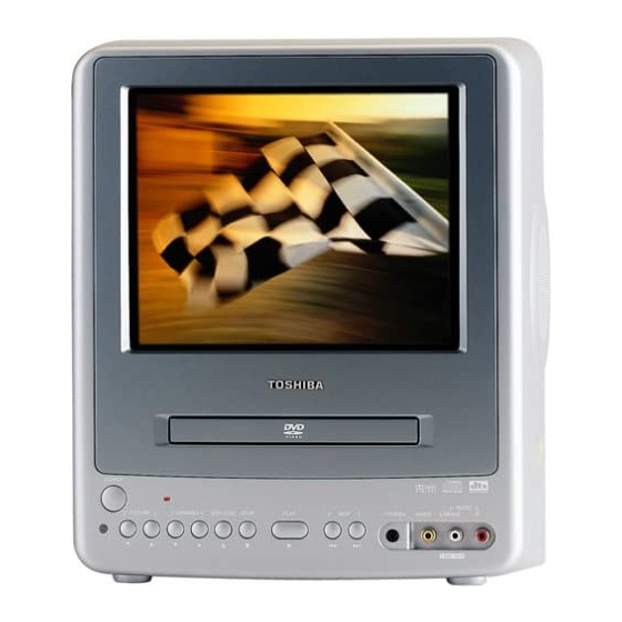
- Page 1 FILE NO. 140-200410 SERVICE MANUAL COLOR TELEVISION/ DVD VIDEO PLAYER MD9DP1 DOCUMENT CREATED IN JAPAN, Feb., 2004...
-
Page 2: Caution
CAUTION THIS DIGITAL VIDEO PLAYER EMPLOYS A LASER SYSTEM. TO ENSURE PROPER USE OF THIS PRODUCT, PLEASE READ THIS SERVICE MANUAL CARE- FULLY AND RETAIN FOR FUTURE REFERENCE. SHOULD THE UNIT REQUIRE MAINTENANCE, CONTACT AN AUTHORIZED SERVICE LOCATION-SEE SERVICE PROCEDURE. USE OF CONTROLS, ADJUSTMENTS OR THE PERFORMANCE OF PROCEDURES OTHER THAN THOSE SPECIFIED HEREIN MAY RESULT IN HAZARDOUS RADIATION EXPOSURE. -
Page 3: How To Order Parts
SERVICING NOTICES ON CHECKING 1. KEEP THE NOTICES 6. AVOID AN X-RAY As for the places which need special attentions, Safety is secured against an X-ray by consider- they are indicated with the labels or seals on the ing about the cathode-ray tube and the high cabinet, chassis and parts. -
Page 4: Important Safeguards
IMPORTANT SAFEGUARDS READ INSTRUCTIONS All the safety and operating instructions should be read before the unit is operated. RETAIN INSTRUCTIONS The safety and operating instructions should be retained for future reference. HEED WARNINGS All warnings on the unit and in the operating instructions should be adhered to. FOLLOW INSTRUCTIONS All operating and use instructions should be followed. - Page 5 IMPORTANT SAFEGUARDS (CONTINUED) DAMAGE REQUIRING SERVICE Unplug this unit from the wall outlet and refer servicing to qualified service personnel under the following conditions: When the power-supply cord or plug is damaged. If liquid has been spilled, or objects have fallen into the unit. If the unit has been exposed to rain or water.
-
Page 6: Disc Removal Method At No Power Supply
DISC REMOVAL METHOD AT NO POWER SUPPLY Remove the Back Cabinet and AV PCB/DVD Block. (Refer to item 1 of the DISASSEMBLY INSTRUCTIONS.) Slide the Rack Loading (White) toward the arrow direction by using a minus driver to release the lock. (Refer to Fig. -
Page 7: Table Of Contents
TABLE OF CONTENTS CAUTION ..........................A1-1 SERVICING NOTICE ON CHECKING ................... A1-2 HOW TO ORDER PARTS ...................... A1-2 IMPORTANT SAFEGUARDS ....................A1-3, A1-4 DISC REMOVAL METHOD AT NO POWER SUPPLY ............A1-5 PARENTAL CONTROL-RATING LEVEL ................A1-5 TRAY LOCK ..........................A1-5 TABLE OF CONTENTS ...................... -
Page 8: General Specifications
GENERAL SPECIFICATIONS CRT Size / Visual Size 9 inch / 228.6 mmV System CRT Type Normal Deflection 90 degree Magnetic Field BV/BH +0.45G / 0.18G Color System NTSC Speaker 2 Speaker Position Side Size 3 inch Impedance 8 ohm Sound Output 1.2W + 1.2W 10%(Typical) 0.8W + 0.8W... - Page 9 GENERAL SPECIFICATIONS Temperature Operation +5oC ~ +40oC Storage -20oC ~ +60oC Operating Humidity Less than 80% RH On Screen Menu(TV) Display Menu Type Icon TV Setup Picture Audio Picture Preference Channel Setup TV/CATV Auto CH Memory Add/ Delete V-chip Setup Language Sleep Timer CH / AV(LINE) / DVD...
- Page 10 GENERAL SPECIFICATIONS G-10 On Screen Menu (DVD) Display Menu Type Character Language Menu Subtitle Audio Picture TV Screen Size OSD Display On/Off JPEG Interval Select Files Sound DRC (Dynamic Range Control) dts Decode Output(5.1ch/ 2ch) Surround On/Off Center On/Off Sub Woofer On/Off Parental Password Lock/ Un Lock Rating Level...
- Page 11 GENERAL SPECIFICATIONS G-13 Remote Unit RC-GD Control Glow in Dark Remocon Format Custom Code 71-8E h Power Source Voltage(D.C) UM size x pcs UM-4 x 2 pcs Total Keys 45 Key Keys Power Play Stop Search+ Search- Skip+ Skip- Slow+ Slow- Pause Call...
- Page 12 Auto Setup Audio DAC 192kHz / 24bit G-15 Accessories Owner's Manual Language English w/Guarantee Card Buyer Model No. MD9DP1 Remote Control Unit Battery UM size x pcs UM-4 x 2 pcs OEM Brand Rod Antenna Poles Terminal Loop Antenna Terminal...
- Page 13 Dimensions W x D x H(mm) 338x381x386 Design As Per Buyer 's Description of Origin Buyer Model No. MD9DP1 Drop Test Natural Dropping At 1 Corner / 3 Edges / 6 Surfaces Height (cm) Container Stuffing (40' container) 1260 Sets...
-
Page 14: Disassembly Instructions
DISASSEMBLY INSTRUCTIONS 1-3: TV/DVD BLOCK (Refer to Fig. 1-3) 1. REMOVAL OF MECHANICAL PARTS Remove the 2 screws 1. AND P.C. BOARDS Disconnect the following connectors: 1-1: BACK CABINET (Refer to Fig. 1-1) (CP301, CP302, CP401 and CP403). Remove the 5 screws 1. Remove the TV/DVD Block in the direction of arrow. - Page 15 DISASSEMBLY INSTRUCTIONS 1-5: FRONT TRAY PLATE/TOP SHIELD Pick Up PCB (Refer to Fig. 1-5) Unlock the 2 supports 1. Remove the Front Tray Plate in the direction of arrow (A). Remove the 12 screws 2. Remove the Top Shield in the direction of arrow (B). DVD Deck Make the sort circuit using a soldering.
-
Page 16: Removal Of Dvd Deck Parts
DISASSEMBLY INSTRUCTIONS 2. REMOVAL OF DVD DECK PARTS Main Chassis Ass’y NOTE 1. Do not disassemble the DVD DECK PARTS except listed Rack Loading parts here. Minute adjustments are needed if the disas- semble is done. If the repair is needed except listed parts, replace the DVD MECHA ASS’Y. - Page 17 DISASSEMBLY INSTRUCTIONS NOTE Main Chassis Ass'y When installing the Clamper Magnet, install it with the green face up. When installing the wire of the Lever Switch, install it correctly as Fig. 2-4-B. When installing the Lever Switch, install it correctly as Traverse Holder Fig.
- Page 18 DISASSEMBLY INSTRUCTIONS NOTE 2-9: GEAR (Refer to Fig. 2-9-A) Unlock the support 1. After the assembly of the Rack Feed, check if the Rack Feed 1/2 is moving smoothly. (Refer to Fig. 2-7-B) Remove the Middle Gear 1/2/3, Idler Gear and Feed Gear. In case of the Rack Feed Ass’y installation, install cor- rectly as Fig.
- Page 19 DISASSEMBLY INSTRUCTIONS 2-11: FEED MOTOR (Refer to Fig. 2-11-A) Remove the 2 screws 1. Remove the Feed Motor. Remove the Motor Gear. Main Chassis Ass'y Motor Gear Feed Motor • Screw Torque: 1 ± 0.5kgf•cm Fig. 2-11-A NOTE In case of the Motor Gear installation, check if the value of the Fig.
-
Page 20: Removal Of Anode Cap
DISASSEMBLY INSTRUCTIONS 3. After one side is removed, pull in the opposite direction to 3. REMOVAL OF ANODE CAP remove the other. Read the following NOTED items before starting work. NOTE After turning the power off there might still be a potential Take care not to damage the Rubber Cap. -
Page 21: Removal And Installation Of Flat Package Ic
DISASSEMBLY INSTRUCTIONS 3. When IC starts moving back and forth easily after 4. REMOVAL AND INSTALLATION OF FLAT desoldering completely, pickup the corner of the IC using PACKAGE IC a tweezers and remove the IC by moving with the IC REMOVAL desoldering machine. - Page 22 DISASSEMBLY INSTRUCTIONS INSTALLATION 4. When bridge-soldering between terminals and/or the soldering amount are not enough, resolder using a Thin- 1. Take care of the polarity of new IC and then install the tip Soldering Iron. (Refer to Fig. 4-8.) new IC fitting on the printed circuit pattern. Then solder each lead on the diagonal positions of IC temporarily.
-
Page 23: Service Mode List
SERVICE MODE LIST This unit provided with the following SERVICE MODES so you can repair, examine and adjust easily. To enter to the SERVICE MODE function, press and hold both buttons simultaneously on the main unit and on the remote control for more than a standard time (second). -
Page 24: When Replacing Eeprom(Memory) Ic
WHEN REPLACING EEPROM (MEMORY) IC If a service repair is undertaken where it has been required to change the MEMORY IC, the following steps should be taken to ensure correct data settings while making reference to TABLE 1. NOTE: No need setting for after INI 27 due to the adjustment value. Table 1 Enter DATA SET mode by setting VOLUME to minimum. -
Page 25: Electrical Adjustments
ELECTRICAL ADJUSTMENTS BEFORE MAKING ELECTRICAL FUNCTION FUNCTION ADJUSTMENTS OSD H COL. AV(CENT.) OSD CONTRAST COL. AV(MAX) Read and perform these adjustments when repairing the CUT OFF COL. AV(MIN) H POSITION TINT AV circuits or replacing electrical parts or PCB assemblies. H BLK L SHARPNESS AV H BLK R... - Page 26 ELECTRICAL ADJUSTMENTS 2-4: WHITE BALANCE 2-8: VERTICAL LINEARITY NOTE: Adjust after performing CUT OFF adjustment. NOTE: Adjust after performing adjustments in section 2-7. After the adjustment of Vertical Linearity, reconfirm Place the set with Aging Test for more than 15 minutes. the Vertical Position and Vertical Size adjustments.
- Page 27 ELECTRICAL ADJUSTMENTS 2-10: OSD HORIZONTAL 2-13: TINT CENTER Receive the color bar pattern. (RF Input) Activate the adjustment mode display of Fig. 1-1. Using the remote control, set the brightness, contrast, Press the VOL. UP/DOWN button on the remote control until the difference of A and B becomes minimum.
- Page 28 ELECTRICAL ADJUSTMENTS 2-14: COLOR CENTER 2-15: CONTRAST MAX Receive the color bar pattern. (RF Input) Activate the adjustment mode display of Fig. 1-1 and Using the remote control, set the brightness, contrast, press the channel button (22) on the remote control to color and tint to normal position.
- Page 29 ELECTRICAL ADJUSTMENTS PURITY AND CONVERGENCE 3-3: STATIC CONVERGENCE ADJUSTMENTS NOTE Adjust after performing adjustments in section 3-2. NOTE Receive the crosshatch pattern from the color bar Turn the unit on and let it warm up for at least 30 generator. minutes before performing the following adjustments.
- Page 30 ELECTRICAL ADJUSTMENTS 4. ELECTRICAL ADJUSTMENT PARTS LOCATION GUIDE (WIRING CONNECTION) CD803 CD802 CRT PCB CP803B CP802B TP022 J801 TP024 POWER PCB J3801 J4201 CP3001 FB401 CP402 CD3001 CP803A CP3802 CD805 D3824 CP802A CP401 SPEAKER CP403 CD3801 CP302 AC IN VR401 SPEAKER J2203 J2204...
- Page 31 DVD BLOCK DIAGRAM FLASH 64M SDRAM IC4007 IC4005 SST39VF800A- M12L64164A-7T 70-4C-EK HA0~HA20, SDA0~SDA11 HD0~HD15 VCR BLOCK CD4002 DVD LOADER DM II RFA_SDEN, DATA, SCLK A, B, C, D, E, F READ AAF_CE, FE, TE, PI Pick up CHANNEL FNN, FNP IC2601 P.CON+3.3V CD, DVD, LD...
- Page 32 TV BLOCK DIAGRAM RESET IC IC103 PST3231NR POWER TU001 ON/OFF OPEN/CLOSE MICON IC IC101 STOP OEC6079A X101 16MHz PLAY Q105 SKIP FF V-BUFFER 6 11 12 40 41 SKIP REW FROM DVD BLOCK CVBS DVD C DVD Y DVD_RESET R.OUT G.OUT V801 B.OUT...
- Page 33 POWER BLOCK DIAGRAM SOUND+B UNREG+8V F3801 D3840~D3843 TRANSFORMER SWITCHING RECTIFIER AC IN T3802 IC3803 Q3810 PS2561L1-1-V(W) Q3811, Q3812 FEED BACK FEED BACK VR3802 UNREG+5V UNREG+12V VR3801 TRANSFORMER SWITCHING T3801 J3801 Q3808 DC JACK PROTECTOR 11.3V REG OPE AMP RY3801 IC3802 NJM2368D Q3806 RELAY DC POWER...
-
Page 34: Dvd
PRINTED CIRCUIT BOARDS DVD (BOTTOM SIDE) DVD (TOP SIDE) R2330 R2337 R2331 R2325 C2312 B2604 C2306 C2311 R2328 R2327 C2309 C2310 C2643_1 HS2301 R2324 R2334 R2326 R2648 R2345 R2322 C2305 R2319 W864 C4080 C2644_1 C2649 R2321 R2318 R2344 C2646_1 R2316 IC4003 C4012 R2611... - Page 35 PRINTED CIRCUIT BOARDS AV/CRT (INSERTED PARTS) SOLDER SIDE IC301 CP301 CP8002 C2204 CP8001 W068 Q3002 R303 W046 IC3005 S803Y R301 W031 C130 W047 W090 L3001 W839 W048 W059 C303 W060 W158 R3002 R3001 W061 SW2220 S803X R3003 W168 R346 Q3006 Q3009 R2201 W102...
- Page 36 PRINTED CIRCUIT BOARDS AV/CRT (CHIP MOUNTED PARTS) SOLDER SIDE Q403 R816 Q601 R632 Q605 Q602 R142 R634 R622 Q4201 R4246 R611 R610 R125 R608 R103 Q106 R150 IC4202 IC103 R115 Q105 IC902 IC903 IC904 R916 Q4206 R4229 R147 R4239 Q4207 Q901 R4240 R323...
- Page 37 PRINTED CIRCUIT BOARDS POWER RELAY (INSERTED PARS) SOLDER SIDE SOLDER SIDE W853 R3811 D3814 D3839 R3802 D3833 Q3808 R3822 R3807 W036 R3806 R3809 D3809 R3808 R3818 W822 C3823 C3803 D3844 C3818 W004 CP3803 W801 W005 W006 R3815 IC3803 D3807 W007 C3811 W002 W012...
-
Page 38: Mpeg/Micon
MPEG/MICON SCHEMATIC DIAGRAM (DVD PCB) FROM/TO AUDIO/VIDEO DAC_VIDEO_C DAC_VIDEO_B C4038 DAC_VIDEO_D C4088 R4002 +-1% ASDATA0 0.01 B +-1% 0.01 B R4003 ABCLK ALRCLK DUPTD1 C4089 R4004 +-1% AMCLK DUPRD1 R4005 +-1% 0.01 B DUPTD0 C4090 W832 V_GND DUPRD0 0.01 W833 RESET P.CON+5V P.CON+3.3V... -
Page 39: Memory
MEMORY SCHEMATIC DIAGRAM (DVD PCB) FLASH IC 8M FROM/TO MPEG/MICON IC4007 SST39VF800A-70-4C-EK SD_A0 SD_A1 HA16 HA15 SD_A2 SD_A3 C4064 SD_A4 HA14 VCCQ SD_A5 64M SDRAM IC 0.1 F SD_A6 IC4005 SD_A7 HA13 M12L64164A-7T SD_A8 SD_A9 SD_A10 HD15 HA12 DQ15 SD_A11 SD_D15 SD_D0 DQ15... -
Page 40: Rf Amp/Dsp
RF AMP/DSP SCHEMATIC DIAGRAM (DVD PCB) FROM/TO MPEG/MICON FROM/TO LODER SPDL_SENS TOUT_SW R2625 MOT_SPDL+ TIN_SW FFC(P=0.5mm) RFA_SDEN 4.7K R2627 R2626 R2631 MOT_SPDL- RFA_DATA P.CON+5V RFA_SCLK CD2601 4.7K 1.5K AAF_CE 2H0O1901 AAF_FE R2620 AAF_TE VR DVD CTL +IN2 -IN2 OUT2 CP2601 AAF_PI Q2603 4.7K... -
Page 41: Audio/Video
AUDIO/VIDEO SCHEMATIC DIAGRAM (DVD PCB) W876 DAC_C[C]_VIDEO W877 DAC_B[Y]_VIDEO FROM/TO MPEG/MICON W879 P.CON+A5V DAC_D_DVD_VIDEO P.CON+A5V DAC_VIDEO_C DAC_VIDEO_B DAC_VIDEO_D P.CON+5V P.CON+3.3V C8505 DAC_VIDEO_C RESET VIDEO_BUFFER 12P CH Q8502 L8502 KTA1504S_Y_RTK 0305 AMCLK VIDEO_BUFFER ABCLK Q8503 ALRCLK KTA1504S_Y_RTK C8508 ASDATA0 DAC_VIDEO_B 12P CH L8503 1uH 0305 C8511... - Page 42 REGULATOR1 SCHEMATIC DIAGRAM (AV PCB) FROM POWER CP3001 (CP3803) B2013H02-8P SOUND_GND SOUND GND SOUND+B SOUND+B TO SOUND AMP UNREG+5V UNREG+5V UNREG+5V SOUND+B POWER_FAIL P.FAIL SOUND_GND UNREG+12V UNREG+12V UNREG+8V UNREG+8V 5VREG. IC UNREG+12V IC3001 KIA7805API 3.3V OUT Q3003 UNREG+8V KTB1366 DRIVER 3.3V CTL Q3012 Q3006...
- Page 43 MICON/TUNER SCHEMATIC DIAGRAM (AV PCB) TU001 115-V-K015AR_B FROM/TO IN/OUT C006 C002 6.3V I2C_OFF 0.1 B REMOCON D106 KEY_A R150 R151 KEY_B MTZJ10B POWER_ON_H 1/4W EXT_MUTE Q106 KTA1504S_Y_RTK FROM/TO CHROMA X101 1002T01606 R140 CSTLS16M0X53-A0 OSD_Y R144 D101 OSD_B R141 2.7K OSD_G 1SS133 R145 2.7K...
- Page 44 CHROMA SCHEMATIC DIAGRAM (AV PCB) FROM/TO REGULATOR1 DVD_VIDEO DVD_Y DVD_C UNREG+12V P.CON+5V P.CON+9V AT5.7VREG 8.5VREG R625 FROM/TO DEFLECTION V.OUT H.OUT C4227 R632 C628 FROM/TO IN/OUT CHROMA IC 0.47 W861 DVD_VIDEO IC601 LA76319M-MPB-E VIDEO_OUT FRONT_VIDEO W827 C622 W832 R620 CLMP APC1 1/4W VIDEO CLMP...
- Page 45 SOUND AMP SCHEMATIC DIAGRAM (AV PCB) HS301 763WAA0233 L CH CP301 SP301 SPEAKER TID-X02P-B2 SA08A05BWC SP OUT L+ 8 OHM SP OUT L- R CH CP302 SP302 SPEAKER TID-X02P-B2 SA08A05BWC SP OUT R+ 8 OHM FROM REGURATOR1 SP OUT R- SOUND+B FROM/TO IN/OUT SOUND_L+...
- Page 46 IN/OUT SCHEMATIC DIAGRAM (AV PCB) AT+5.6V OS2202 PIC-37143SY-H REMOCON Vout R2202 AT+5.6V FROM/TO STEREO 1/4W C4201 R4203 AUDIO_OUT_L 560 1/4W C4202 R4204 AUDIO_OUT_R 560 1/4W DVD_AUDIO_L POWER_ON_H R2214_1 R2216_1 DVD_AUDIO_R FRONT_A_IN_L Q2201 R4206 DTC124EKA FRONT_A_IN_R R2218 R2220 R2221 KEY_A 10K 1/4W MUTE SW L4202 Q4205...
- Page 47 STEREO SCHEMATIC DIAGRAM (AV PCB) W862 W868 C920 W867 C940 C942 C922 W871 BUFFER C949 Q901 12.3 12.3 KTA1504S_Y_RTK BUFFER C948 Q902 KTA1504S_Y_RTK L904 D901 100uH 0305 1SS133 FROM/TO MICON/TUNER TUNER_AUDIO R911 100 1/4W R912 100 1/4W TO SOUND AMP R908 P.CON+12V_A A_OUT_L...
- Page 48 DEFLECTION SCHEMATIC DIAGRAM CP403 (AV PCB) A1561WV2-2P DEGAUSS COIL L3800 VRK224-045-15B V.OUTPUT IC W888 IC401 LA78040N-E THERMAL PROTECTION R427 PUMP UP 3.9K 1/4W DEGAUSE SW Q403 DTA114EKA 25.5 12.9 24.8 W884 TO DY FROM/TO MICON/TUNER CP401 B04B-DVS POWER_ON_H X-RAY C423 +30V 250V 0.27...
- Page 49 CRT SCHEMATIC DIAGRAM (CRT PCB) FROM CHROMA CP802B (CP802A) B2013H02-6P CLAMP G.OUT R.OUT B.OUT CLAMP_OFF FROM DEFLECTION CP803B (CP803A) B2013H02-4P HEATER FROM/TO DEFLECTION CP801 (CD805) A2361WV2-2P 120.0 122.0 115.0 RED AMP GREEN AMP BLUE AMP Q804 Q805 Q806 KTC3207 KTC3207 KTC3207 C804 160V...
- Page 50 POWER SCHEMATIC DIAGRAM (POWER PCB) RY3801 ALKS325 D3812 DC JACK J3801 MTZJ6.2B HEC0824-010010 DC POWER SW Q3802 PROTECTOR DC POWER SW. KTC3209_Y Q3803 Q3806 10.9 KRC102MAT KTC3198 R3822 AC_H PROTECTOR/AC,DC SW 100 1/4W Q3808 L3803 KRC102MAT D3803 HF70T22*10*14 MTZJ10B W822 DC_PROTECT C3819 FROM DEFLECTION...
- Page 51 RELAY/SW/FG SCHEMATIC DIAGRAM M2002 M2001 BCD3B02 JCL9B61 (SW PCB) PCB640 BEC001 (RELAY PCB) SW1AB-271-10A IMSA-9615S-08C-PP SLD.MTR(-) SLD.MTR(+) SP.MTR(-) SP.MTR(+) S1005X S1005Y S1005 L.SW S1004X S1004Y S1004 S1001X S1001Y S1001 S1003X S1003Y S1003 PCB68A S1002X S1002Y BEC002 S1002 AWD28 SG-107F6 NOTE:THE DC VOLTAGE AT EACH PART WAS MEASURED NOTE: THIS SCHEMATIC DIAGRAM IS THE LATEST AT THE TIME WITH THE DIGITAL TESTER WHEN THE COLOR BROADCAST OF PRINTING AND SUBJECT TO CHANGE WITHOUT NOTICE...
- Page 52 INTERCONNECTION DIAGRAM DVD PCB POWER PCB PCB020 PCB130 CD2601 VPB164 VMC319 CP2601 CVBS/AUDIO/D.OUT J4201 WHITE YELLOW FRONT VIDEO JACK FRONT AUDIO JACK FRONT AUDIO JACK CP3803 CP3001 J2203 J2204 J2202 SOUND GND SOUND GND MON(DVD) MON(DVD) SOUND+B SOUND+B NC(SW) NC(SW) UNREG+5V UNREG+5V VOL(DVD)
-
Page 53: Micon/Tuner
WAVEFORMS MPEG/MICON 200ns 10ns 100µs 100mV 100mV 200mV AUDIO/VIDEO 10µs 500µs 100ns 100mV 500mV 100mV MICON/TUNER MEMORY POWER ON 500µs 0.2ms 500mV 200mV RF AMP/DSP POWER ON 10µs 200ns 0.2ms 200mV 500mV NOTE: The following waveforms were measured at the point of the corresponding balloon number in the schematic diagram. -
Page 54: Chroma
WAVEFORMS POWER ON STANDBY POWER ON 10ms 0.5µs 0.2ms 0.5V 50mV POWER ON POWER ON 10µs POWER ON 20µs 0.5V POWER ON POWER ON POWER ON 50µs 20µs 10µs CHROMA SOUND AMP POWER ON POWER ON POWER ON 20µs 10µs 0.5V 100mV NOTE:... -
Page 55: In/Out
WAVEFORMS POWER ON POWER ON 20µs 100mV 200mV IN/OUT POWER ON DVD PLAY POWER ON 20µs 0.5ms 200mV 200mV DEFLECTION DVD PLAY POWER ON POWER ON 0.5ms 20µs 200mV STEREO POWER ON POWER ON 20µs 50mV NOTE: The following waveforms were measured at the point of the corresponding balloon number in the schematic diagram. -
Page 56: Mechanical Exploded View
MECHANICAL EXPLODED VIEW PCB110 (CRT PCB ASS'Y) 101G 101F 101E 101C 101B 101D 101A I1-1... - Page 57 MECHANICAL EXPLODED VIEW PCB020 (POWER PCB ASS'Y) PCB130 (DVD PCB ASS'Y) PCB250 (AV PCB ASS'Y) I1-2...
- Page 58 MECHANICAL EXPLODED VIEW (PACKING DIAGRAM) 125, 131, 132, 133, 134, BL001, CD504, TM101 I1-3...
-
Page 59: Dvd Deck Exploded View
DVD DECK EXPLODED VIEW CD2302 Do not replace the parts. Because, minute adjustments are needed if CD2001 this condition is disassembled further more. PCB640 If the repair is needed, replace the (SW PCB ASS'Y) DVD MECHA ASS'Y. M2602 PCB68A (RELAY PCB ASS'Y) CD2301 NOTE: Applying positions AA for the grease are... -
Page 60: Mechanical Replacement Parts List
MECHANICAL REPLACEMENT PARTS LIST Location No. TSB P/N Reference No. Description AE003132 7A701A029A FRONT CABI ASS'Y 101A AE003133 701WPJC512 CABINET,FRONT 101B AE001206 713WPA0259 GLASS,LED 101C AE001207 713WPA0260 GUIDE,REMOCON 101D AD302193 7235490034 BADGE,BRAND 101E AE003134 735WPBA962 BUTTON,FRAME 101F AE001209 738WPA0065 STOPPER,BUTTON 101G AE000174 800WQ00056... -
Page 61: Dvd Deck Replacement Parts List
DVD DECK REPLACEMENT PARTS LIST Location No. TSB P/N Reference No. Description AE003142 A2D001A650 DVD MECHA ASS'Y A2D001A650 AD301822 92P100022A TRAVERSE HOLDER AE002480 92P100080A RACK,FEED 1A AE002481 92P100081A RACK,FEED 2A AD301825 92P100035A LEVER,RACK FEED AD301826 92P200006A INSULATOR(F) AD301827 92P200007A INSULATOR(R) AD301846 92P100029A GEAR,FEED... -
Page 62: Electrical Replacement Parts List
ELECTRICAL REPLACEMENT PARTS LIST Location No. TSB P/N Reference No. Description RESISTORS ! R401 AD301016 R3X28A331J R,METAL OXIDE 330 OHM 2W ! R402 BZ210280 R3X28A391J R,METAL OXIDE 390 OHM 2W R408 BZ210083 R3X28A010J R,METAL OXIDE OHM 2W ! R415 AD302063 R4X5T44R7F R,METAL 4.7 OHM 1/4W... - Page 63 ELECTRICAL REPLACEMENT PARTS LIST Location No. TSB P/N Reference No. Description DIODES ! D416 BZ410020 D97U05R11B DIODE,ZENER MTZJ5.1B T-77 D603 BZ410085 D2WXN40050 DIODE,SILICON 1N4005-EIC D801 BZ410006 D1VT001330 DIODE,SILICON 1SS133T-77 D802 BZ410006 D1VT001330 DIODE,SILICON 1SS133T-77 D803 BZ410006 D1VT001330 DIODE,SILICON 1SS133T-77 D901 BZ410006 D1VT001330 DIODE,SILICON...
- Page 64 ELECTRICAL REPLACEMENT PARTS LIST Location No. TSB P/N Reference No. Description ! IC3002 BZ611015 I1KA97805A KIA7805API ! IC3005 BZ611033 I1KA97809A KIA7809API ! IC3802 BZ611096 I0QD023680 NJM2368D ! IC3803 AD301771 000220001W PHOTO COUPLER PS2561L1-1-V(W) IC4001 AE000842 ICQK067620 ZR36762 IC4002 BZ611124 I5HJ004BF0 S-24C04BFJ-TB IC4003 BZ611130...
- Page 65 ELECTRICAL REPLACEMENT PARTS LIST Location No. TSB P/N Reference No. Description TRANSISTORS Q4212 BZ510109 TCAA3875SY TRANSISTOR,SILICON KTC3875S_Y_RTK Q8502 BZ510108 TAAA1504SY TRANSISTOR,SILICON KTA1504S_Y_RTK Q8503 BZ510108 TAAA1504SY TRANSISTOR,SILICON KTA1504S_Y_RTK Q8504 BZ510108 TAAA1504SY TRANSISTOR,SILICON KTA1504S_Y_RTK COILS &TRANSFORMERS L001 BZ310156 021375101K COIL 100 UH L101 BZ310030 021LA6560K...
- Page 66 ELECTRICAL REPLACEMENT PARTS LIST Location No. TSB P/N Reference No. Description MISCELLANEOUS B3806 BZ310121 024HT03553 CORE,BEADS W5RH3.5X5X1.0 B4001 BZ310186 024HC31022 CORE,BEADS FCM2012H-102T04 B4002 BZ310186 024HC31022 CORE,BEADS FCM2012H-102T04 B4003 BZ310186 024HC31022 CORE,BEADS FCM2012H-102T04 B4004 BZ310186 024HC31022 CORE,BEADS FCM2012H-102T04 B4005 BZ310186 024HC31022 CORE,BEADS FCM2012H-102T04 B4006...
- Page 67 ELECTRICAL REPLACEMENT PARTS LIST RESISTOR RC....CARBON RESISTOR CAPACITORS CC....CERAMIC CAPACITOR CE....ALUMI ELECTROLYTIC CAPACITOR CP....POLYESTER CAPACITOR CPP....POLYPROPYLENE CAPACITOR CPL....PLASTIC CAPACITOR CMP....METAL POLYESTER CAPACITOR CMPL....METAL PLASTIC CAPACITOR CMPP....METAL POLYPROPYLENE CAPACITOR J3-6...
- Page 68 TOSHIBA CORPORATION 1-1, SHIBAURA 1-CHOME, MINATO-KU, TOKYO 105-8001, JAPAN...
Need help?
Do you have a question about the MD9DP1 and is the answer not in the manual?
Questions and answers