LG GSA-5163D Service Manual
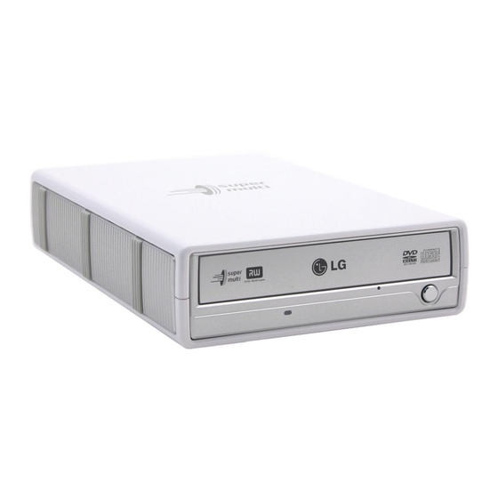
External super multi dvd rewriter
Hide thumbs
Also See for GSA-5163D:
- Owner's manual (15 pages) ,
- Specifications (2 pages) ,
- Owner's manual (15 pages)

Related Manuals for LG GSA-5163D


Summary of Contents for LG GSA-5163D
- Page 1 External Super Multi DVD Rewriter S E RVICE MANUAL MODEL: GSA-5163D P/NO : 3828HS1050B March, 2005 Printed in Korea MODEL : GSA-5163D...
-
Page 2: Table Of Contents
TABLE OF CONTENTS SECTION 1 : GENERAL INTRODUCTION ..................................3 GENERAL FEATURES .................................3~4 SPECIFICATIONS.................................5~8 OPERATING MANUAL ...............................9~17 DISASSEMBLY ..................................18 1. TOP COVER ...................................18 2. INTERNAL DVD MULTI DRIVE ............................18 3. USB/1394 BRIDGE BOARD............................18 EXPLODED VIEW ................................19~20 REPLACEMENT PARTS LIST..............................21 BLOCK DIAGRAM[USB/1394 BRIDGE BOARD] ........................22 CIRCUIT DIAGRAM[USB/1394 BRIDGE BOARD] ......................23~31 SECTION 2 : DVD MULTI DRIVE ASSY DISASSEMBLY .................................32~33... -
Page 3: Section 1 : General
SECTION I GENERAL INTRODUCTION This service manual provides a variety of service information. It contains the mechanical structure of the External Super Multi DVD Rewriter and the electronic circuits in schematic form. This External Super Multi DVD Rewriter was manufactured and assembled under our strict quality control standards and meets or exceeds industry specifications and standards. - Page 4 4. Performance 1) Average access time: DVD-ROM 145 ms (1/3 stroke) CD-ROM 125 ms 2) Write speed: DVD-R 2x, 4x CLV, 8x ZCLV, 16x PCAV DVD-RW 1x, 2x, 4x, 6xCLV DVD-RAM 2x, 3x ZCLV (Ver.2.2), 3x-5x PCAV(Ver.2.2) DVD+R 2.4x, 4x CLV, 8x ZCLV, 12x, 16x PCAV DVD+R DL 2.4x, 4x CLV DVD+RW...
-
Page 5: Specifications
SPECIFICATIONS I. MODEL : GSA-5163D 1. SYSTEM REQUIREMENTS -CPU: IBM Compatible Pentium 4 2.8GHz (or faster) -512MB Memory or greater 2. SUPPORTING OPERATING SYSTEM * Operating System * Recording tool Window 2000 Professional (1) Nero(Ahead) Window XP Home Edition, Professional... - Page 6 2.3 Disc diameter ..........120mm 80mm (Horizontal only) 2.4 Data capacity • User Data/Block DVD-ROM/R/RW/RAM/+R/+RW ..2,048 bytes/block CD (Yellow Book) ..........2,048 bytes/block(Mode 1 & Mode 2 Form 1) 2,336 bytes/block (Mode 2) 2,328 bytes/block (Mode 2 Form 2) 2,352 bytes/block (CD-DA) 2.5 RPC (Regional Playback Control) Phase2, No Region 3.
- Page 7 3.3 Data transfer rate 3.3.1 Sustained transfer rate <Write> DVD-R......2.77, 5.54, 8.31-11.08 Mbytes/s.........2x, 4x CLV, 8x ZCLV 9.14-22.16 Mbytes/s ..............16x PCAV DVD-RW ....1.385, 2.77, 5.54, 8.31 Mbytes/s ........1x, 2x, 4x, 6x CLV DVD-RAM(Ver. 2.2): ...2.77, 4.15, 4.15-6.925 Mbytes/s ..2x, 3x ZCLV, 3-5PCAV(w/o Verify) DVD+R ......3.32, 5.54 5.
-
Page 8: Power Requirements
5. POWER REQUIREMENTS 5.1 Power Requirements AC Adaptor INPUT : 100-240V AC, 50/60Hz OUTPUT : 5V/12V 1.5A * Which is not provided with Circuit Diagram of this model. Please Contact the friendly staff of LG Service Care at: Website http: //www.LGEservice.com... -
Page 9: Operating Manual
OPERATING MANUAL Contents Introduction System requirements ................10 Important precautions ................11 Location and function of controls ...............12 Installation Hardware Installation ................13 Removing the USB converter cable ............14 Operation Loading and ejecting a disc ...............15 Playing a music CD..................16 Playing DVD video and MPEG2 movie video ...........16 Appendix Troubleshooting ..................17 WARNING: Only drives bearing the logo Compact Disc ReWritable Ultra Speed... -
Page 10: System Requirements
Windows 2000 Professional/XP(Home Edition/ Professional), Software Required Direct X 9.0 or Higher is required. CD-R, CD-RW, CD-R : LG, Mitsubishi Chemical, Verbatim, Taiyo Yuden, TDK DVD-R, DVD-RW, or SKC discs are recommended. DVD+R, DVD+RW, CD-RW : LG, Ricoh, Mitsubishi Chemical, Verbatim discs are DVD-RAM discs recommended. - Page 11 Follow these precautions when handling the drive or discs. Precautions Please note that the manufacturer of this equipment does not offer any warranty against data loss due to inappropriate installation, handling, direct or indirect damages. Please note that the manufacturer will bear no responsibility for direct or indirect damages (including lost data)caused by the use of this product or its malfunction.
- Page 12 This dr iv e should be used only in its current hardware and softw are configur ation. 1. Disc Tray 2. Drive activity indicators The LED used to indicate the oper ation of External Super Multi DVD Rewriter. Read: The green color is displayed during disc reading session. Write: The green color is flashed during disc writing sessions.
- Page 13 Installation NOTES Connecting to computer • Make sure you have a personal computer with an open USB port or IEEE 1394 port before connecting the drive to your computer. ON OFF • You cannot use the FireWire [IEEE 1394] and USB interfaces simultaneously.
- Page 14 The drive supports the plug and play(not swap) function of Windows, and can be removed and inserted by performing the following operation. 1. Stop the application softwre being currently used. 2. Clic k the icon " " of the taskbar located on your screen's bottom right side .
- Page 15 Operation Remember - AC adapter must be connected. Make sure the power is turned on. 1. Push the Eject Button to open the Disc tray. 2. Load a disc. (Label facing up.) 3. Close the Disc tray. 1. Push the Eject Button to open the Disc tray. 2.
- Page 16 When connected to a computer, you can play audio CD’s through your computer’s audio system after setting Digital Audio mode. Check your Windows or “Windows Media Player” manual for detail. The drive must be connected to a computer, and basic installation already done.
-
Page 17: Troubleshooting
Appendix Troubleshooting If you are experiencing problems with the drive, verify the following items. Since the problem may be caused by a device other than the drive, check other things such as system settings or other software being used, etc. If you cannot resolve the problem after verifying these items, contact your dealer or our customer service department. -
Page 18: Disassembly
DISASSEMBLY 1. TOP COVER 3. USB/I1394 BRIDGE BOARD A. Remove 6 side rubbers and release 8 screws(A). A. Remove Top Shield and Plate Assembly. B. And then, remove 2 side panels and Top cover in B. Release 4 screws(B) and remove the USB/1394 the direction of arrow(1).(see Fig.1-1) bridge board in the direction of arrow(3).(See Fig. -
Page 19: Exploded View
EXPLODED VIEW PBS00(USB/1394 C.B.A) -
Page 20: Replacement Parts List
MECHANICAL REPLACEMENT PARTS LIST • MODEL: GSA-5163D LOCA.NO PART NO(GS) DESCRIPTION SPECIFICATION REMARKS ASSEMBLE PARTS SECTION 6779H-1020A DVD MULTI DRIVER ASSY JRP3 GSA-5163D PARTS SECTION 3551H-1032C COVER ASSEMBLY TOP(JRP3) 3551H-1031B COVER ASSEMBLY BOTTOM(JRP3) GSA-5163D 5040H-1100A RUBBER SIDE HOOT(JRP1) 3550H-1112A COVER... -
Page 21: Block Diagram[Usb/1394 Bridge Board]
BLOCK DIAGRAM (USB2.0/1394 BRIDGE BOARD) +3.3V +3.3V FLASH EEPROM 39VF010 INTERFACE 24LC02B A0-A14 D0-D7 CHIP +3.3V PL-3507 V BUS DMARS DPRS D0-D7 CTL0-CTL1 CPNA CRYSTAL 12MHZ PORT LINKON XTPA0+ XTPA0- FW802B CRYSTAL XTPB0+ 1394 PORT1 24.576MHZ XTPB0- XTPBIAS0 V BUS XTPA1+ XTPA1- XTPB1+... -
Page 22: Circuit Diagram[Usb/1394 Bridge Board]
CIRCUIT DIAGRAM(USB2.0/1394 BRIDGE BOARD) IDERSTJ FIRE_DIO[0] GP1[0] D0_LU IDERSTJ DIOWJ FIRE_DIO[1] GP1[1] D1_LU -RESET DIORJ GP1[2] FIRE_DIO[2] D2_LU DD07 DD08 DMACKJ GP1[3] FIRE_DIO[3] D3_LU DD06 DD09 IORDY PD10 GP1[4] FIRE_DIO[4] D4_LU DD05 DD10 10 INTRQ PD11 GP1[5] D5_LU DD04 DD11 5.6k FIRE_DIO[5] PD12... - Page 23 XTPBIAS1 330PF/NA 0.1uF 0.33uF 2.49K 56.1% 56.1% BEAD/0805 1394VCC XTPA1+ 0R/NA TPA+ 0R/NA 3.3V XTPA1- TPA- 0R/NA XTPB1+ TPB+ A3.3V 0R/NA XTPB1- TPB- SCLK_LU BEAD 24.576M Hz SHLD SHLD 15pF 56.1% 56.1% C27PF C27PF 1394 6PIN connector BEAD COMMON CHOKES CASE1 0.1uF LREQ_LU...
- Page 24 A3.3V 3.3V BEAD/0805 VOUT BEAD ADJ(GND) AIC 1117 0.1uF 0.1uF 10uF/10V 10uF/10V 0.1uF 0.1uF L20 BEAD/NA BEAD/NA 0.1uF/NA BEAD/NA L22 BEAD/NA PHONE JACK STEREO/NA PIN header/NA 15pF/NA 15pF/NA 0R/NA 0.1uF/NA 0R/NA 0.1uF/DIP R78 0R/1206/NA POWER ON 0R/1206/NA L23 BEAD/DIP R80 3.3K BEAD/0805/NA JS1 M-DIN_5-R BEAD/0805...
-
Page 25: Section 2 : Dvd Multi Drive Assy
SECTION II DVD MULTI DRIVE ASSY DISASSEMBLY 1. CABINET and CIRCUIT BOARD 1-3. Cabinet and Main Circuit Board A. Remove the Cabinet in the direction of arrow (4). DISASSEMBLY (See Fig. 1-3) 1-1. Bottom Chassis B. Release 2 hooks (a) and remove the CD Tray A. - Page 26 2-2. Pick-up A. Release 1 screw (C) and remove the Pick-up. Pick-up Unit Pick-up Fig. 2-2...
-
Page 27: Exploded View
EXPLODED VIEW PBM00 (MAIN C.B.A) PBF00 (FRONT C.B.A) -
Page 28: Description Of Circuit
DESCRIPTION OF CIRCUIT 1. ALPC (Automatic Laser Power Control) Circuit 1-1. Block Diagram... - Page 29 1-2. ALPC (Automatic Laser Power Control) Circuit ALPC function DVD/CD anlaog front-end IC(IC101 HD153722TF) is for constant power control purpose. Based on the accurate power sensor(FMON) in P/U, ALPC feedback loop maintains constant power level against laser diode’s temperature variation. The ALPC loop amplifies(10x) the FMON signal to enhance the accuracy of read power level control.
-
Page 30: Focus Circuit
2. Focus Circuit 2-1. Block Diagram DVD : A1+A2+A3+A4 CD : EF1+EF2+EF3+EF4 (EF1~EF4) HAVC A1~A4 0.8V IC101 HD153722TF HAVC B1~B4 (EF1~EF4) R334 Disc DVD : (B1+B3)-(B2+B4) Optical CD : (EF1+EF3)-(EF2+EF4) Motor unit Pick-up C325 HOP-8541T Focusing Compensator IC301 FACT- FACT+ R8J32005FP R615 FOIN... - Page 31 3. Tracking & Sled Circuit 3-1-1. Block Diagram (Tracking Following) IC101 HD153722TF MPPO (A+D)-(B+C) HAVC SPPO A1~A4 (F, E) DVD : (A1+A4)-(A2+A3) Disc R337 Optical CD : (EF1+EF2)-(EF3+EF4)-K*(E-F) Motor unit Pick-up HOP-8541T C328 Tracking Compensator TACT- TACT+ Sled IC301 Compensator R8J32005FP SLED MOTOR Unit...
- Page 32 3-1-2. Block Diagram (Seek) IC101 HD153722TF MPPO (A+D)-(B+C) (EF1~EF4) HAVC SPPO A1~A4 (F, E) K*{(F+H)-(E+G)} Disc Optical VREF1 C114 Motor unit Pick-up (A+D)-(B+C) HOP-8541T TEIN K*{(F+H)-(E+G)} VREF1 TACT- TACT+ HAVC MIRR MIRR SUMF BOTTOM RFIP HOLD HOLD SLED MOTOR RFIN Unit MIRRTOPH MIRRBOTH...
- Page 33 3-2-1. Tracking Servo The aim of tracking servo is to make laser beam trace the data track on disc. Tracking Error(TE) Signal is generated from tracking error detected block in HD153722 using DPP(Differential Push-Pull) Method(CD) and PP(Push-Pull) Method(DVD). DPP Method uses not only main beam(EF1~EF4) but also side beam(E, F) for correcting DC offset generated in Push-Pull Method.
-
Page 34: Spindle Circuit
4. Spindle Circuit 4-1-1. Block Diagram(FGCAV Servo) Optical Pick-up HOP-8541T Disc Motor unit X301 33.8688MHz VCK4M IC301 Control Clock R8J32005FP Generator CAV FD R330 CAV PD VCK4M R326 R329 Motor Kick 3.3V C319 1.65V SPIN IC601 DAVC 1.65 M63041AFP CTL1 CTL1 CTL2 CTL2... - Page 35 4-2-1. Block Diagram (Wobble CLV Servo) C119 C120 C121 WAG1 WAG2 WAG3 21 22 AGC1 AGC2 Disc Motor uni t Optical Pick-up AGC3 HOP-8541T WOBSIG WBLSH IC101 WBLSH VREF HD153722TF IC301 R8J32005FP R336 C319 Motor Kick 1.65V 4-2-2. Wobble CLV Servo DVD-RAM: 2x, 3x, 5x / DVD-R: 8x, 4x, 2x / DVD+R: (GSA-5120D : 12x, 8x, 4x, 2.4x, GSA-5160D : 16x, 8x, 4x, 2.4x)
-
Page 36: Major Ic Internal Block Diagram And Pin Description
MAJOR IC INTERNAL BLOCK DIAGRAM AND PIN DESCRIPTION IC101 (HD153722TF) : RF AMP Analog Signal Processor Pin Assignment SUMF/SUMF2 RFIP MCLK IP1/LPPOUT/AWOBSIGD RFIN SRVREF IP2/MIRR FVREFO WOBSIG IREFT RDGATE VREF1 LO_ZB/SPDSH HAVC IDGATE HAVC2 RFHLD/TISH1 HD153722TF BLANK PWDETO (TOP VIEW) GND4 (3.3V)VDD2 RLDON... - Page 37 Block Diagram *3300p *3300p/0.1u Lo-Z Function by IDGATE MREF1 fast mode „ = 3.3us 0.47u (*2) *3300p/0.068u 4700p (Ri=1k/20k switch) molk to MIRR DEFECT 0.068u RFIP EQOR RF SUM/SUB RFIN EQON (RGA) SUBP,N AUTO 0.068u SUMF2 EQOS to WRF IP1/LFPOUT/AWOBSIGD ATEST LPPMON/EQOS/RRF/WRF IP2/MIRR...
- Page 38 • Pin Description Pin no. Pin Name Type Function WRFIS Analog-Input WRF single input terminal. LE/LPS_A Analog-Output Lens error and lens shift signal output terminal. LPS_B/ADIN0 Analog-Output Lens shift and Renesas test signal output terminal. Analog-Output Focus error output terminal. PE/ADIN1 Analog-Output PE and Renesas test signal output terminal.
- Page 39 Pin no. Pin Name Type Function RLDON Digital-Input Input terminal to control laser driver output for APC read. GND4 Ground Ground connection terminal[digital]. Digital-Output Tracking zero cross signal digital output terminal. PWDETO Digital-Output Laser diode over power detection output terminal. BLANK Digital-Output Record/non-record detecting output terminal / BD...
- Page 40 Pin no. Pin Name Type Function IREFE External-resistor required Terminal to connect RF-equalizer fc setting extermal resistor. GND1 Ground Ground connected terminal. EQON Differential-Output RF Equalizer differential output terminal. EQOP Differential-Output RF Equalizer differential output terminal. VDD1 External capacitor required Terminal to connect AGC-DET input high pass filter capacitor.
- Page 41 IC301 (R8J32005FP) : Encoder, Decoder & DSP Singal Processor 1.1 Pin Layout VSSR DOUT VCCI0 VCCR VSSI0 MRSTB TESTB1 IOCS16B VSSRQ HINTRQ TESTB2 DACKB TEST0 IORDY VCCRQ ZIORB TEST1 ZIOWB TEST2 DREQ TEST3 DATA15 VSSRQ DATA0 HEATRUN DATA14 CSEL DATA1 AMUTE VCCI0 VCCI0...
- Page 42 1.2 Block Diagram VREF, VREFC VREF33 BIAS VIBIAS LOUT AUDIO ROUT EFMP DOUT EFMN Data DFF[1:0] DREQ JFF[1:0] DACKB CD-ROM DASPB DCLPF[2:0] CS3FXB Data DRLPF[2:0] CS1FXB VISTRB PDIAGB MONANA[1:2 ATAPI W1LPF[2:0] CD-DSP WPLL Jitter IOCS16B W2LPF[2:0] HINTRQ IORDY ZIORB ZIOWB Wobble WOBSIG HRSTB...
- Page 43 1.3 Pin Table Pin No. Pin Name Pin No. Pin Name Pin No. Pin Name Pin No. Pin Name VSSR LOADOUT SDATA DCLK DOUT LOADIN SCLK VCCA VCCR VSSRQ FEMCK VCCA EJECTSW RDGATE MRSTB ACTFLG LOWZB TESTB1 DRVEN1 IDGATE SIGM VSSRQ VCCRQ RFHLD...
- Page 44 Pin No. Pin Name Pin No. Pin Name Pin No. Pin Name Pin No. Pin Name VCCA DATA7 PDIAGB W1LPF2 DATA8 W1LPF1 DATA6 W1LPF0 DATA9 CS1FXB CPU15 VSSA DATA5 CS3FXB CPU14 VREFC DATA10 DASPB CPU13 VIBIAS DATA4 UCS1B CPU12 VREF DATA11 UCS0B CPU11...
- Page 45 1.4 Pin Functions It corresponds to the following signs as a pin I/O specification. AI : Analog Input IOU : Standard Input/Output with Pull Up AO : Analog Output 5I : 5V Tolerant Input AIO : Analog Input/Output 5O : 5V Tolerant Output Standard Input 5TO : 5V Tolerant Three State Output...
- Page 46 1.4.2 Servo Pin List Pin Name Pin No. Destination Function DEFECT Defect (scratch detect) signal BLANK Blank signal input (also connected to the H8S interrupt port INT5) Tracking Zero Crossing signal input DRVR Spindle FG pulse (also input to the H8S interrupt port INT4) DRVR Tilt drive signal (PWM output) DRVR...
- Page 47 1.4.3 ATAPI Interface Pin List Pin Name Pin No. Destination Function HRSTB ATAPI ATAPI IF control signal (host reset signal) ATAPI ATAPI IF register address signal DATA[15:0] 180, 178, ATAPI ATAPI IF data bus 172, 170, 168, 166, 164, 162, 161, 163, 165, 167, 169, 171,...
- Page 48 1.4.4 Encoder Interface Pin List Pin Name Pin No. Destination Function IP1LPPIN PID area identification signal/LPP input signal IP2MIRR PID area identification signal/MIRR signal WOBSIG Wobble signal input LSRERR Laser error signal RDGATE PLL input switch signal LOWZB Input impedance switch control signal/SPDSH; running OPC sampling pulse (Pit top) IDGATE ID/data switch signal/wobble signal sampling pulse 2...
- Page 49 1.4.5 Serial Communication Interface Pin List Pin Name Pin No. Destination Function LDBUSY LDD serial IF busy WDEN LDD microcomputer I/F (transfer enable signal) RFDEN AFE/LDD microcomputer I/F (transfer enable signal) SDATA AFE / LDD AFE/LDD microcomputer I/F (transfer data signal 3V system) SCLK AFE / LDD...
- Page 50 1.4.8 H8S Micro-Processor Pin List (a) CPU Pin Name Pin No. Destination Function HEATRUN ATAPI CPU general port 1- 0: Off heat run test input CSEL ATAPI CPU general port 1- 6: ATAPI CSEL AMUTE Audio Mute ckt CPU general port 0- 2: Audio mute CSW3 CPU general port 1- 7: Cartridge detect signal 3 CSW2...
- Page 51 (b) Flash/SRAM Pin Name Pin No. Destination Function UCS1B SRAM H8S/CS1, also functions as the CPU general port 2- 0 UCS0B Flash H8S/CS0 CPWRB Flash/SRAM H8S/WRB CPRDB Flash/SRAM H8S/RDB A[20] Flash/SDRAM H8S/A[20] A[19:17] 204, 205 H8S/A[19:17] A[16:0] 207, 208 H8S/A[16:0] 209, 210 211, 212 215, 216...
- Page 52 1.4.9 LSI/TEST Control Pin List Pin Name Pin No. Destination Function ROMICE Non-maskable CPU interrupt port (sensed at the falling edge) MRSTB RESET IC Master reset input TESTB1 Test select TESTB2 TEST0 User test/CPU general port 2 TEST1 Test monitor can be set as the following table by a register.
- Page 53 1.4.10 Power Supply/GND Pin List Pin Name Pin No. Function 32, 53, DSP core power supply (1.5V) 173, 188, VCCR 3, 62 SDRAM power supply (3.3V) VCCRQ 10, 23, SDRAM I/O power supply (3.3V) 31, 39. VDDAA 1.5V system analog power supply (1.5V) WPLL1, 2 VCCA Analog power supply (3.3V) : Dedicated for LVDS Analog power supply (3.3V) : Servo A/D...
- Page 54 IC601 (M63041AFP) : SPINDLE MOTOR AND 6CH ACTUATOR DRIVER Block Diagram For LOADING 4.5-5.5V For/FO/TR/TILT 7-13.2V 4.5-5.5V For SPINDLE Current gain 3A/V 7-13.2V H Bridge Voltage gain Voltage gain Voltage gain SWICHING Commutation CIRCUIT Frequency OPOUT 150KHz Current gain commutation Current gain 0.44[0.88]A/V 0.44[0.88]A/V...
- Page 55 Input/Output circuit diagram SPIN, SL1IN, SL2IN FOIN, TOIN, TLIN EN1, EN2 LOIN OPIN- 5VCC 5VCC 5VCC 5VCC SLGS ACTFLG, FG ACTRST OPOUT 5VCC 5VCC 5VCC 5VCC 5VCC 5VCC 5VCC VM1, U, V, W VM2, SL1+, SL1-, SL2+, SL2- SL1+ SL1- SL2+ SL2- 5VCC, FO+, FO-, TO+, TO-, TL+, TL-...
- Page 56 IC302 (MBM29LV160BE) : Flash Memory Pin Assignment TSOP(1) (Marking Side) BYTE N.C. RESET Normal Bend N.C. N.C. RT/BY (FPT-48P-M19)
- Page 57 Block Diagram to DQ RY/BY RY/BY Buffer Erase Voltage Input/output Generator Buffer State BYTE Control RESET Command Register Program Voltage Generator Chip Enable Data Latch Output Enable Logic Y-Decoder Y-Gating Timer for Address Low Vcc Detector program/Erase Latch X-Decoder Cell Matrix to A...
- Page 58 • Pin Description Function to A Address Inputs to DQ Data Inputs/Outputs Chip Enable Output Enable Write Enable RY/BY Ready/Busy Output RESET Hardware Reset Pin/ Temporary Sector Unprotection BYTE Select 8-bit or 16-bit mode N.C. Pin Not Connected Internally Device Ground Device Power Supply •...
-
Page 59: Troubleshooting Guide
TROUBLESHOOTING GUIDE (01) Laser Power Adjust (using RD Power/WR Power/Erase Power) MPU & DSP IC301 Pickup Setting Pin#106 pin#112 Front Monitor Driver IC101 IC201 (02) High Frequency/NRZI skew Adjust Pickup 45-49 MPU & DSP Driver IC301 (03) Data Slice/Equalizer Boost/Raw Slice/ Equalizer Frequency Adjust MPU &... - Page 60 (06) Focus Amp. and Total Amp. Adjust All Disc Setting Pin# Pickup 85-98 FE:R334,C325 IC101 MPU & DSP IC301 PE:R335,C326 Focus:#34-35 R346, Driver C338 IC601 (07) Tracking Amp. Adjust All Disc Setting Pin# Pickup 85-98 IC101 TE:R337,C328 MPU & DSP IC301 Tracking #30-31...
- Page 61 (10) Unwritten Slice Level Adjust for DVD-RAM DVD-RAM Disc Pin# Setting 77-78 IC101 Pickup MPU & DSP IC301 SIGMON:R336, C327 #102 Slider FPC Slider:#6, 8-10 Driver IC601 (11) Focus Offset Adjust for DVD-ROM, CD-R/RW DVD-ROM Disc Pin# Setting 85-98,77-78 IC101 Pickup MPU &...
- Page 62 (14) Tilt Adjust for DVD-RAM DVD-RAM Disc Pin# Setting Pickup 85-98,77-78 IC101 TCPH:R340, C331 MPU & DSP IC301 TIE:R341,C333 Slider FPC Driver Slider:#6, 8-10 IC601 (15) Tilt Adjust for DVD-R/RW, DVD+R/RW, CD-R/RW DVD-R/RW Disc Pin# Setting 85-98, 77-78 IC101 TE:R337, C328 MPU &...
- Page 63 (18) Lens Sensitivity Adjust Pickup (Temp.Information) #113 IC301 (19) Spindle Offset Adjust Pin# Spindle 12-14 Driver MPU & DSP IC601 IC301 SPD:R330,C319 (20) ADIP BPF/Read Timing Adjust for DVD+R/RW DVD+R Disc Setting Pin# 85-98,77-78 IC101 Pickup MPU & DSP WobSIG IC301 #46 #46 Slider FPC...
- Page 64 (22) RTZ TimeOut Fail & Slider/ Slider FPC Driver Spindle Slider:#6,8-10 IC301 IC601 Spindle FFC (23) Focus Servo/Tracking Servo Fail All Disc Pin# Setting 85-98 IC101 FE:R334,C325 Pickup MPU & DSP IC701 TE:R337,C328 Focus:#34-35 Tracking:#30-31 PE:R335,C326 R346,C338 Slider FPC Driver Slider:#6,8-10 IC601 R348, C339...
- Page 65 Detail Error Code & Fail Analysis 1. Laser Power Initial Adjust Error Code Contents of fail Fail Analysis Block Diagram SSB Byte8,9 28xx LP Adjust NG. 1) Check Pickup FFC Connection. No.01 (Exchange 2) Check solder of IC101circumference. low/high byte) (pin#10, 14, 16, L150, L151) 3) Check solder of IC201.
- Page 66 2. Adjusting Error during Disc Load Sequence (Lead in Error) No. Error Code Contents of fail Fail Analysis Block Diagram SSB Byte21,22 42xx Circuit Offset Adjust NG. 1) Check Pickup FFC Connection. No.04 2) Check solder of IC101circumference . (pin#,4,5,6 pin#85-98, FE_Servo: R334, C325 TE_Servo: R337, C328 PE_Servo: R335, C326)
- Page 67 No. Error Code Contents of fail Fail Analysis Block Diagram SSB Byte21,22 47xx Servo Loop Gain Adjust NG. 47XA: Disc Unmatch(Exchange Disc). No.9 1) Check Pickup FFC Connection. 2) Exchange Pickup (Signal Noisy). 3) Check solder of IC101circumference. (pin#4,5,6 pin#85-98, FE_Servo: R334, C325 TE_Servo: R337, C328) 4) Exchange IC101(AFE).
- Page 68 No. Error Code Contents of fail Fail Analysis Block Diagram SSB Byte21,22 182x Home Position Adjust NG. 1) Check FFC Connection. No.22 01xx (DVD-SL Only) 2) Check Slider FPC Connection. 3) Exchange Slider Motor. 4) Check solder of IC101circumference. 5) Exchange IC101(AFE). 52xx Focus Offset Adjust NG.
- Page 69 No. Error Code Contents of fail Fail Analysis Block Diagram SSB Byte21,22 59xx Spindle Offset Adjust NG. 1) Check Spindle FFC Connection. No.19 2) Check solder of IC601circumference. (pin#12-14) 3) Exchange IC601(Driver). 4) Exchange Spindle Motor. 5) Check solder of IC301circumference. 6) Exchange IC301(DSP).
- Page 70 3. Loading Sequence Error (Lead in Error) No. Error Code Contents of fail Fail Analysis Block Diagram SSB Byte21,22 2503,2504 RTZ Timeout(Sled Timeout). 1) Check Slider FPC Connection. No.22 2) Check solder of IC601 circumference . (pin#2-3, 6, 8-10) 3) Exchange IC601. 4) Exchange Slider Motor.
- Page 71 Power Supply System Diagram Line-in IC601 Driver (M63041FP) L601 VM1 #22 Spindle VM2 #05 Slide BD9703FP[ROHM] IC702 Pick_up (CN101) VSO(5.3) VSO #42 (#13) DDcon 5VR(5.3) L151 IC101 AFE (HD153722TF) 5.3V VCC IC102 Analog SW (HD74LV2G53A) VCC #8 IC103 Analog SW (HD74LV2G53A) Q202 VCC #8 (OPEN) Q203...
- Page 72 PCB Poor Analysis - Check list Circuit/IC Signal Signal/Level mesurement-point (IC-pin or Device) Power supply Line-12V CN108-41 Line-5V CN108-44 (IC701) reg-5.3V 5.3V R711 (IC702) reg-3.3V 3.3V (IC703) reg-1.5V 1.5V reg-2.8V 2.8V Flash-ROM VDD : 3.3V 3.3V (IC302) Active-Low read-CK VDD : 1.5V 1.5V 32, 53,128, 213, 173, 188 (IC301)
- Page 73 HW Self- Diagnostic function 1. Self-Diagnostic Function by LED Blink. • Basic operation: MPU is included in DSP, MPU accesses each peripheral (inside, exterior) device, and discover a defect by the ability of a read/write of data to be performed correctly. Since MPU operates by the program with a built-in Flash-ROM, when abnormalities are in MPU, Flash-ROM, and these Data-Bus &...
- Page 74 2. LED does not blink at all at the time of a power supply injection. Eject-SW does not react. (1) Is it normal to the exterior Bus (Data-Bus, Address-Bus, control signal system) of MPU? Viewing — check: -- a short circuit, opening, etc. •...
- Page 75 3. Motor, Abnormalities in Actuator System The drive circuit of a motor & actuator consists of the three ICs IC601 (M63041AFP). The work of each IC is as follows. (1) IC601(M63041AFP) : 7ch driver Spindle motor driver: 180° audio drive Type, an analog input, a PWM drive, a Vm=12V. Stepping motor driver X2: analog input, a PWM drive (differential), a Vm=12V Loading motor driver: Input/Output PWM drive, Vm=5V.
-
Page 76: Block Diagram
BLOCK DIAGRAM Flash-ROM (2MByte) MBM29LV160BE OPU:HOP-8541T or Equivalent (HITACHI ME) (FUJITSU) Disc Interface Loading motor connector Analog Front End DVD/CD DSP Analog HD153722TF (DVD/CD/Servo/ATAPI) audio Disc R8J32005FP 100pin-TQTF Slide motor 256pin LQFP motor (RENESAS) Unit (RENESAS) mechanism DVD-codec Host IDE CD-codec LPP/ADIP decorder 7ch-Driver...
Need help?
Do you have a question about the GSA-5163D and is the answer not in the manual?
Questions and answers